US6584159B1 - Mixed-mode next/echo canceller for pulse amplitude modulated (PAM) signals - Google Patents
Mixed-mode next/echo canceller for pulse amplitude modulated (PAM) signals Download PDFInfo
- Publication number
- US6584159B1 US6584159B1 US09/188,625 US18862598A US6584159B1 US 6584159 B1 US6584159 B1 US 6584159B1 US 18862598 A US18862598 A US 18862598A US 6584159 B1 US6584159 B1 US 6584159B1
- Authority
- US
- United States
- Prior art keywords
- signal
- mixed
- tap
- error
- crosstalk
- Prior art date
- Legal status (The legal status is an assumption and is not a legal conclusion. Google has not performed a legal analysis and makes no representation as to the accuracy of the status listed.)
- Expired - Lifetime
Links
Images


Classifications
-
- H—ELECTRICITY
- H04—ELECTRIC COMMUNICATION TECHNIQUE
- H04B—TRANSMISSION
- H04B3/00—Line transmission systems
- H04B3/02—Details
- H04B3/20—Reducing echo effects or singing; Opening or closing transmitting path; Conditioning for transmission in one direction or the other
- H04B3/23—Reducing echo effects or singing; Opening or closing transmitting path; Conditioning for transmission in one direction or the other using a replica of transmitted signal in the time domain, e.g. echo cancellers
Definitions
- the present invention relates generally to crosstalk cancellation techniques and more particularly, to methods and apparatus for reducing near-end crosstalk (NEXT) and echo crosstalk in the continuous time domain.
- NXT near-end crosstalk
- FIG. 1 illustrates a hybrid transceiver 100 that transmits and receives signals on the same twisted pair (TP) 110 .
- the hybrid transceiver 100 is commonly associated with a local area network (LAN) or digital subscriber loops (xDSL).
- the main sources of crosstalk in such a transceiver 100 are usually near-end crosstalk (NEXT) and Echo crosstalk.
- Each hybrid transceiver, such as the transceiver 100 transmits a first signal, V 1 , and receives a different signal, V 2 , on the same twisted pair 110 .
- Near-end crosstalk results from transmitting and receiving different signals on different twisted pairs 110 and having a signal on one twisted pair interfering with the signal on another twisted pair.
- V 1 corresponds to the transmitted signal generated by the transceiver 100 .
- V 2 corresponds to the received signal generated by a second transceiver 120 . Since the transceiver 100 knows the transmitted signal, V 1 , that it has generated, the transceiver 100 can subtract the transmitted signal, V 1 , from the voltage (V 1 +V 2 ) on the twisted pair (TP) 110 , to obtain the voltage corresponding to the received signal V 2 .
- Echo crosstalk is the result of crosstalk on the same twisted pair 110 and of discontinuous impedances along a given path, for example, at each connector.
- each impedance discontinuity along the path causes the transceiver 100 to receive a wave or echo back.
- FIG. 2 corresponds to the impulse response 200 of an impulse signal transmitted along the twisted pair (TP) 110 by the transceiver 100 .
- each peak 210 - 213 in the impulse response 200 corresponds to a different connector (not shown) on the twisted pair (TP) 110 .
- the impulse response 200 is utilized to obtain the echo path and then adjust the taps of an echo canceller (not shown) to the peaks of the echo impulse response.
- the taps are adjusted, for example, using the well known least mean square (LMS) algorithm, to match the energy and delay of the echo canceller to the peaks of the echo impulse response.
- LMS least mean square
- the tap values converge and remain constant.
- the impulse response is static and coincides w with the symbol rate.
- the echo canceller can be implemented using low cost, low power digital circuitry.
- the transmitter and receiver are not synchronized and the resulting impulse response is dynamic. In such an asynchronous communication system, a frequency offset exists between the transmitter and the receiver.
- FIR finite impulse response
- a mixed-mode crosstalk canceller that performs crosstalk cancellation in the continuous time domain.
- the disclosed mixed-mode crosstalk canceller processes the pulse amplitude modulated (PAM) digital signal to be transmitted as well as the received signal to compensate for the crosstalk between the transmit and receive signals.
- the output of the crosstalk canceller is subtracted from the received signal in the continuous time domain.
- the transmit symbol clock and the receive symbol clock can be asynchronous.
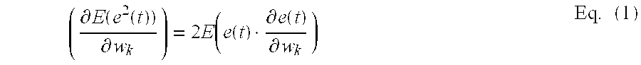
- the tap weights for the crosstalk cancellation are obtained using a modified version of the least mean square (LMS) algorithm for discrete time signals.
- LMS least mean square
- the modified least mean square (LMS) algorithm is applied for continuous time signals that are derived from different clocks, using the following equation:
- w k ( n +1) w k ( n )+ ⁇ ⁇ tilde over (e) ⁇ ( t ) ⁇ x k ( t )
- the LMS algorithm requires a costly multiplication of the error signal, e(t), and the digital transmit signal.
- x k (t) Since it is only necessary to go in the direction of the gradient with the steepest decent, however, computational gains are achieved in accordance with the present invention using a correlation multiplier that quantizes e(t) and x k (t) with only one or two bits, and performs the correlation multiplication using an asynchronous logic circuit.
- the correlation multiplier receives a 2 bit quantized representation of the digital transmit signal.
- x k (t) and a 1 bit quantized version of the error signal, e(t).
- the quantized version of the error signal, e(t) indicates the sign of the error (positive or negative) and is obtained in the illustrative embodiment by comparing the error signal to zero.
- a crosstalk canceller that updates each tap weight utilizing the disclosed correlation multiplier that provides a signal indicating whether the tap weight needs to be increased or decreased to a charge pump that produces a current in-the proper direction.
- FIG. 1 illustrates a conventional hybrid transceiver that transmits and receives signals on the same twisted pair (TP);
- FIG. 2 illustrates the impulse response of an impulse signal transmitted along the twisted pair (TP) of FIG. 1 by the transceiver;
- FIG. 3 illustrates a stream of asynchronous crosstalk pulses at two different instants of time, t 1 and t 2 ;
- FIG. 4 illustrates a schematic block diagram of a mixed-mode crosstalk canceller in accordance with the present invention
- FIG. 5A provides the mapping of the digital transmit signal, x k , to the two bit quantized values a 0 and a 1 used in the circuitry of FIG. 5B;
- FIG. 5B illustrates the logic circuitry for the correlation multiplier of FIG. 6
- FIG. 6 illustrates a mixed-mode crosstalk canceller in accordance with the present invention
- FIG. 7 is a block diagram of the update circuit of FIG. 6;
- FIG. 8 is a block diagram of the analog tap of FIG. 6;
- FIG. 9 illustrates the logic circuitry of the multiplying digital-to-analog converter (DAC) of FIG. 8;
- FIG. 10 is a set of sample tables illustrating the thermometer code to symbol mapping in the multiplying digital-to-analog converter (DAC) of FIG. 9 .
- a mixed-mode crosstalk canceller that allows crosstalk cancellation in the continuous time domain.
- the present invention permits asynchronous signals to be processed. It is noted that a number of modem standards, such as 100 Base Tx, allow the transmitter and receiver to be asynchronous, making digital crosstalk cancellation difficult.
- FIG. 3 shows a stream of asynchronous crosstalk pulses at two different instants of time, t 1 and t 2 . Due to the frequency offset between the transmit clock and the receive clock, the crosstalk impulses are sampled at different phases, s 1 through s 4 , for times t 1 and t 2 . Thus, the received signal is sampled by the transceiver 100 with a time-varying phase.
- FIG. 4 shows a schematic block diagram of a mixed-mode crosstalk canceller 400 in accordance with the present invention.
- the input, X, of the mixed-mode crosstalk canceller 400 is a digital number representing an N-level pulse amplitude modulated (PAM) signal to be transmitted.
- a pulse-shaping filter 410 can be placed before or after the digital-to-analog converter (DAC) 420 , depending on whether the pulse shaping is performed on the signal in digital or analog form.
- the architecture of the mixed-mode crosstalk canceller 400 is independent of the pulse shaping, since the pulse-shaping filter 410 can be considered part of the crosstalk channel.
- the mixed-mode crosstalk canceller 400 also includes a track and hold amplifier 430 and an analog-to-digital converter (ADC) 440 .
- ADC analog-to-digital converter
- the mixed-mode crosstalk canceller 400 includes a crosstalk canceller 600 , discussed further below in conjunction with FIG. 6, to compensate for the crosstalk between the transmit and receive signals. Since the output of the crosstalk canceller 600 is subtracted from the received signal in the continuous time domain, the transmit symbol clock and the receive symbol clock can be asynchronous.
- x k and e can be asynchronous signals.
- Equation 2 requires the knowledge of a reference signal.
- R is available at start-up.
- updates can usually not be performed during a normal data transmission mode.
- Equation 6 the second term is equal to zero since R and x are uncorrelated signals (receive symbols and transmit symbols are uncorrelated). Therefore, the conventional tap update algorithm can be modified to:
- Equation 7 is very similar to the expression of the LMS tap update for discrete time signals, with e(t) and x k (t) being continuous time, sampled and held cyclostationary signals that are derived from different clocks. Since it is difficult to multiply ⁇ tilde over (e) ⁇ (t) times x k (t), and it is only necessary to go in the direction of the gradient with the steepest decent, ⁇ tilde over (e) ⁇ (t) and x k (t) can be quantized with a small number of bits, and the correlation multiplication can be performed using an asynchronous logic circuit.
- FIGS. 5A and 5B show an illustrative implementation of a correlation multiplier 500 for implementing Equation 5, where 1 bit is used to represent the sign of the error signal, ⁇ tilde over (e) ⁇ (t), and x k (t) is represented by 2 bits ( ⁇ 1, 0).
- the mapping for the correlation multiplier 500 is shown in FIG. 5 A and the corresponding logic circuitry is shown in FIG. 5 B.
- the correlation multiplier 500 includes a pair of exclusive OR gates 510 , 515 , a pair of inverters 520 , 525 , and a pair of AND gates 530 , 535 .
- the input to the correlation multiplier 500 can be continuous.
- FIG. 6 illustrates an analog implementation of the crosstalk canceller 600 , discussed above in conjunction with FIG. 4 .
- the crosstalk canceller 600 includes a quantizer 610 to reduce the N-level digital symbol X to a few bits.
- the quantizer 610 quantizes the X value to 2 bits (a 0 a 1 ).
- the quantized value is then applied to an update circuit 700 - 702 , such as the update circuit 700 discussed below in conjunction with FIG. 7 .
- the update circuit 700 updates the corresponding tap value by dynamically determining the appropriate tap weight, w N .
- the analog taps 800 - 802 such as the analog tap 800 discussed below in conjunction with FIG. 8, receive the N-level digital symbol X and weight, w N . as inputs and produces an output current, I N .
- the crosstalk canceller 600 includes subtractor circuitry for implementing equation 6 .
- the subtractor circuitry includes an op-amp 620 and an analog comparator 630 that produce a one-bit value representative of the sign of the error signal.
- the crosstalk canceller 600 also includes a number of digital delays, D, in a known manner.
- FIG. 7 illustrates an update circuit 700 of FIG. 6 .
- the update circuit 700 includes a correlation multiplier 500 , discussed above in conjunction with FIG. 5 B.
- the correlation multiplier 500 determines the optimum tap weights by generating a signal 10 indicating whether the tap weight values need to be increased or decreased to move in the direction of the gradient.
- the charge pump 710 may be embodied as a charge pump used for phase locked loop (PLL) circuits that generates a positive or negative current in response to the signal from the correlation multiplier 500 .
- the step size of the least mean square (LMS) algorithm can be adjusted by sizing the current in the charge pump 710 .
- the loop filter 720 is a proportional plus integral loop filter.
- FIG. 8 illustrates the analog tap 800 of FIG. 6.
- X k is an N-level signal, represented by a 0 , . . . ,a N ⁇ 1 .
- w k V CTRL less V REF .
- the analog tap 800 includes two cross-coupled multiplying digital to analog converters (MDAC) 900 , 901 to generate signed weight values, w k , by current subtraction.
- MDAC digital to analog converters
- the output current of the analog tap 2800 , Iout equals lout p minus Iout n and is approximately proportional to (Vctrl minus Vref) multiplied by X, where X is the digital input with thermometer representation a 0 ,a 1 , . . . a N ⁇ 1 .
- Vctrl ⁇ Vref For large voltage differences (Vctrl ⁇ Vref) the relation between lout and (Vctrl ⁇ Vref) may be a non-linear function, F. However, due to the existence of a tap update feed-back loop proper convergence of the tap weights is guaranteed, provided that the non-linear function, F, is monotonic.
- the multiplying digital-to-analog converter (DAC) 900 of FIG. 8 can be implemented using the well-known current steering DAC circuitry of FIG. 9 .
- the MDAC 900 creates an N-level voltage.
- the feedback of FIG. 9 eliminates the digital-to-analog conversion, with the current eventually settling to the proper value.
- the multiplying digital-to-analog converter (NIDAC) 900 includes N parallel tail current sources 910 - 912 controlled by the control voltage Vc. Each tail current is “steered” either towards the positive or negative output terminal of the NIDAC depending on the value of the thermometer code digits a 0 ,a 1 , . . . ,a N ⁇ 1 .
- the resulting differential output current, lout equals Iout p minus Iout n and is proportional to X (a digital input with thermometer code representation a 0 ,a 1 , . . . ,a N ⁇ 1 ).
- the common mode output current (Iout p +Iout n )/2 can be set to a desired value (typically 0) by adjusting the load currents (I BP , I BN ) relative to the tail currents.
Landscapes
- Engineering & Computer Science (AREA)
- Computer Networks & Wireless Communication (AREA)
- Signal Processing (AREA)
- Cable Transmission Systems, Equalization Of Radio And Reduction Of Echo (AREA)
Abstract
Description


Claims (24)
Priority Applications (4)
| Application Number | Priority Date | Filing Date | Title |
|---|---|---|---|
| US09/188,625 US6584159B1 (en) | 1998-11-09 | 1998-11-09 | Mixed-mode next/echo canceller for pulse amplitude modulated (PAM) signals |
| CA002284232A CA2284232A1 (en) | 1998-11-09 | 1999-09-28 | A mixed-mode next/echo canceller for pulse amplitude modulated (pam) signals |
| EP99308675A EP1001553A3 (en) | 1998-11-09 | 1999-11-02 | A mixed-mode next/echo canceller for pulse amplitude modulated (PAM) signals |
| CN99123681.5A CN1258965A (en) | 1998-11-09 | 1999-11-08 | Mixed mode near-end crosstalk/echo eliminator for pulse amplitude modulation signal |
Applications Claiming Priority (1)
| Application Number | Priority Date | Filing Date | Title |
|---|---|---|---|
| US09/188,625 US6584159B1 (en) | 1998-11-09 | 1998-11-09 | Mixed-mode next/echo canceller for pulse amplitude modulated (PAM) signals |
Publications (1)
| Publication Number | Publication Date |
|---|---|
| US6584159B1 true US6584159B1 (en) | 2003-06-24 |
Family
ID=22693923
Family Applications (1)
| Application Number | Title | Priority Date | Filing Date |
|---|---|---|---|
| US09/188,625 Expired - Lifetime US6584159B1 (en) | 1998-11-09 | 1998-11-09 | Mixed-mode next/echo canceller for pulse amplitude modulated (PAM) signals |
Country Status (4)
| Country | Link |
|---|---|
| US (1) | US6584159B1 (en) |
| EP (1) | EP1001553A3 (en) |
| CN (1) | CN1258965A (en) |
| CA (1) | CA2284232A1 (en) |
Cited By (9)
| Publication number | Priority date | Publication date | Assignee | Title |
|---|---|---|---|---|
| US6934387B1 (en) * | 1999-12-17 | 2005-08-23 | Marvell International Ltd. | Method and apparatus for digital near-end echo/near-end crosstalk cancellation with adaptive correlation |
| US20050238125A1 (en) * | 2004-02-02 | 2005-10-27 | Jae-Jin Park | Method of interfacing a high speed signal |
| US20070081475A1 (en) * | 2005-10-11 | 2007-04-12 | Teranetics, Inc. | Multiple modulation rate 10Gbase-T transmission |
| US20080315964A1 (en) * | 2007-06-22 | 2008-12-25 | Dongbu Hitek Co., Ltd. | Voltage controlled oscillator using tunable active inductor |
| US7471670B1 (en) * | 2004-01-20 | 2008-12-30 | Marvell International Ltd. | Method and apparatus for reducing echo and crosstalk in a communication system |
| US20100166096A1 (en) * | 2008-12-31 | 2010-07-01 | Industrial Technology Research Institute | Transmission method and multiple input multiple output wireless communication system using the same |
| US20100309774A1 (en) * | 2008-01-17 | 2010-12-09 | Cambridge Silicon Radio Limited | Method and apparatus for cross-talk cancellation |
| US20100308954A1 (en) * | 2008-01-28 | 2010-12-09 | Uchiya Thermostat Co., Ltd. | Thermal protector |
| US20150131765A1 (en) * | 2013-11-11 | 2015-05-14 | Denso Corporation | Communication apparatus |
Families Citing this family (2)
| Publication number | Priority date | Publication date | Assignee | Title |
|---|---|---|---|---|
| US8126078B2 (en) * | 2003-01-28 | 2012-02-28 | Agere Systems Inc. | Method and apparatus for reducing noise in an unbalanced channel using common mode component |
| US7366231B2 (en) * | 2003-10-28 | 2008-04-29 | Teranetics, Inc. | Sub-block domain transformation multiple signal processing |
Citations (8)
| Publication number | Priority date | Publication date | Assignee | Title |
|---|---|---|---|---|
| WO1989007370A1 (en) | 1988-02-01 | 1989-08-10 | Concord Data Systems, Inc. | Far end echo cancellation method and apparatus |
| US5181198A (en) * | 1991-03-12 | 1993-01-19 | Bell Communications Research, Inc. | Coordinated transmission for two-pair digital subscriber lines |
| EP0727882A2 (en) | 1995-02-17 | 1996-08-21 | Advanced Micro Devices, Inc. | Echo cancellation and suppression |
| US5657384A (en) * | 1995-03-10 | 1997-08-12 | Tandy Corporation | Full duplex speakerphone |
| US5757906A (en) * | 1993-09-10 | 1998-05-26 | Nec Corporation | Method of canceling echoes and echo canceler |
| US5828657A (en) * | 1995-09-29 | 1998-10-27 | Paradyne Corporation | Half-duplex echo canceler training using a pilot signal |
| US5835486A (en) * | 1996-07-11 | 1998-11-10 | Dsc/Celcore, Inc. | Multi-channel transcoder rate adapter having low delay and integral echo cancellation |
| US5937060A (en) * | 1996-02-09 | 1999-08-10 | Texas Instruments Incorporated | Residual echo suppression |
-
1998
- 1998-11-09 US US09/188,625 patent/US6584159B1/en not_active Expired - Lifetime
-
1999
- 1999-09-28 CA CA002284232A patent/CA2284232A1/en not_active Abandoned
- 1999-11-02 EP EP99308675A patent/EP1001553A3/en not_active Withdrawn
- 1999-11-08 CN CN99123681.5A patent/CN1258965A/en active Pending
Patent Citations (9)
| Publication number | Priority date | Publication date | Assignee | Title |
|---|---|---|---|---|
| WO1989007370A1 (en) | 1988-02-01 | 1989-08-10 | Concord Data Systems, Inc. | Far end echo cancellation method and apparatus |
| US5181198A (en) * | 1991-03-12 | 1993-01-19 | Bell Communications Research, Inc. | Coordinated transmission for two-pair digital subscriber lines |
| US5757906A (en) * | 1993-09-10 | 1998-05-26 | Nec Corporation | Method of canceling echoes and echo canceler |
| EP0727882A2 (en) | 1995-02-17 | 1996-08-21 | Advanced Micro Devices, Inc. | Echo cancellation and suppression |
| US5852661A (en) * | 1995-02-17 | 1998-12-22 | Advanced Micro Devices, Inc. | Adaptive echo cancellation used with echo suppression to reduce short and long duration echoes |
| US5657384A (en) * | 1995-03-10 | 1997-08-12 | Tandy Corporation | Full duplex speakerphone |
| US5828657A (en) * | 1995-09-29 | 1998-10-27 | Paradyne Corporation | Half-duplex echo canceler training using a pilot signal |
| US5937060A (en) * | 1996-02-09 | 1999-08-10 | Texas Instruments Incorporated | Residual echo suppression |
| US5835486A (en) * | 1996-07-11 | 1998-11-10 | Dsc/Celcore, Inc. | Multi-channel transcoder rate adapter having low delay and integral echo cancellation |
Cited By (18)
| Publication number | Priority date | Publication date | Assignee | Title |
|---|---|---|---|---|
| US6934387B1 (en) * | 1999-12-17 | 2005-08-23 | Marvell International Ltd. | Method and apparatus for digital near-end echo/near-end crosstalk cancellation with adaptive correlation |
| US7826609B1 (en) | 1999-12-17 | 2010-11-02 | Marvell International Ltd. | Method and apparatus for digital near-end echo/near-end crosstalk cancellation with adaptive correlation |
| US7471670B1 (en) * | 2004-01-20 | 2008-12-30 | Marvell International Ltd. | Method and apparatus for reducing echo and crosstalk in a communication system |
| US8270394B1 (en) | 2004-01-20 | 2012-09-18 | Marvell International Ltd. | Method and apparatus for reducing an interference signal in a communication system |
| US9461703B1 (en) | 2004-01-20 | 2016-10-04 | Marvell International Ltd. | Interference signal compensation |
| US8787861B1 (en) | 2004-01-20 | 2014-07-22 | Marvell International Ltd. | Method and apparatus for reducing echo and crosstalk in a communication system |
| US7593468B2 (en) | 2004-02-02 | 2009-09-22 | Samsung Electronics Co., Ltd. | Method of interfacing a high speed signal |
| US20050238125A1 (en) * | 2004-02-02 | 2005-10-27 | Jae-Jin Park | Method of interfacing a high speed signal |
| US20070081475A1 (en) * | 2005-10-11 | 2007-04-12 | Teranetics, Inc. | Multiple modulation rate 10Gbase-T transmission |
| US7782852B2 (en) * | 2005-10-11 | 2010-08-24 | Teranetics, Inc. | Multiple modulation rate 10Gbase-T transmission |
| US20080315964A1 (en) * | 2007-06-22 | 2008-12-25 | Dongbu Hitek Co., Ltd. | Voltage controlled oscillator using tunable active inductor |
| US20100309774A1 (en) * | 2008-01-17 | 2010-12-09 | Cambridge Silicon Radio Limited | Method and apparatus for cross-talk cancellation |
| US8902724B2 (en) * | 2008-01-17 | 2014-12-02 | Cambridge Silicon Radio Limited | Method and apparatus for cross-talk cancellation |
| US20100308954A1 (en) * | 2008-01-28 | 2010-12-09 | Uchiya Thermostat Co., Ltd. | Thermal protector |
| US8254489B2 (en) * | 2008-12-31 | 2012-08-28 | Industrial Technology Research Institute | Transmission method and multiple input multiple output wireless communication system using the same |
| US20100166096A1 (en) * | 2008-12-31 | 2010-07-01 | Industrial Technology Research Institute | Transmission method and multiple input multiple output wireless communication system using the same |
| US20150131765A1 (en) * | 2013-11-11 | 2015-05-14 | Denso Corporation | Communication apparatus |
| US9306774B2 (en) * | 2013-11-11 | 2016-04-05 | Denso Corporation | Communication apparatus |
Also Published As
| Publication number | Publication date |
|---|---|
| EP1001553A3 (en) | 2000-06-28 |
| CN1258965A (en) | 2000-07-05 |
| EP1001553A2 (en) | 2000-05-17 |
| CA2284232A1 (en) | 2000-05-09 |
Similar Documents
| Publication | Publication Date | Title |
|---|---|---|
| US5157690A (en) | Adaptive convergent decision feedback equalizer | |
| US4539675A (en) | Echo canceller | |
| US5396517A (en) | Transversal filter useable in echo canceler, decision feedback equalizer applications for minimizing non-linear distortion in signals conveyed over full duplex two-wire communication link | |
| EP0111938B1 (en) | Fast convergence method and system for echo canceller | |
| US4571465A (en) | Echo canceller for a baseband data signal | |
| EP0145022B1 (en) | Method and apparatus for cancelling echo | |
| US6584159B1 (en) | Mixed-mode next/echo canceller for pulse amplitude modulated (PAM) signals | |
| US7843859B1 (en) | Analog echo canceller with filter banks | |
| JPH0697729B2 (en) | Self-adaptive equalizer | |
| US5577027A (en) | Apparatus and method for effectively eliminating the echo signal of transmitting signal in a modem | |
| CA2259609A1 (en) | Frequency domain signal reconstruction in sampled digital communications systems | |
| JPS62128627A (en) | Data transmission apparatus | |
| US4769808A (en) | Method of cancelling echoes in full-duplex data transmission system | |
| US4334128A (en) | Echo canceler for homochronous data transmission systems | |
| US6404809B1 (en) | Method and apparatus for training equalizer structures in a digital communication system having periodic digital impairments | |
| US3573624A (en) | Impulse response correction system | |
| CA1194944A (en) | Adaptive filter update normalization | |
| JP2928801B2 (en) | Echo cancellation method and subscriber line audio processing circuit | |
| US4468640A (en) | Adaptive filter update normalization | |
| US7133465B2 (en) | Modified Tomlinson-Harashima precoding method circuit for infinite impulse response (IIR) channels | |
| US20050047532A1 (en) | Apparatus, methods and articles of manufacture for dynamic differential delay correction | |
| US6137809A (en) | Quantization noise compensator apparatus and method | |
| JPS63232631A (en) | Data transmission terminal in bidirectional analog channel | |
| US7212577B2 (en) | Information transfer methods | |
| US6934265B2 (en) | Interference cancellation receiver for high-speed communication systems |
Legal Events
| Date | Code | Title | Description |
|---|---|---|---|
| AS | Assignment |
Owner name: LUCENT TECHNOLOGIES INC., NEW JERSEY Free format text: ASSIGNMENT OF ASSIGNORS INTEREST;ASSIGNORS:AZADET, KAMERAN;INGLIS, DAVID ANDREW;REEL/FRAME:009588/0731 Effective date: 19981106 |
|
| STCF | Information on status: patent grant |
Free format text: PATENTED CASE |
|
| CC | Certificate of correction | ||
| FPAY | Fee payment |
Year of fee payment: 4 |
|
| FPAY | Fee payment |
Year of fee payment: 8 |
|
| AS | Assignment |
Owner name: DEUTSCHE BANK AG NEW YORK BRANCH, AS COLLATERAL AGENT, NEW YORK Free format text: PATENT SECURITY AGREEMENT;ASSIGNORS:LSI CORPORATION;AGERE SYSTEMS LLC;REEL/FRAME:032856/0031 Effective date: 20140506 Owner name: DEUTSCHE BANK AG NEW YORK BRANCH, AS COLLATERAL AG Free format text: PATENT SECURITY AGREEMENT;ASSIGNORS:LSI CORPORATION;AGERE SYSTEMS LLC;REEL/FRAME:032856/0031 Effective date: 20140506 |
|
| AS | Assignment |
Owner name: AGERE SYSTEMS LLC, PENNSYLVANIA Free format text: CERTIFICATE OF CONVERSION;ASSIGNOR:AGERE SYSTEMS INC.;REEL/FRAME:034113/0626 Effective date: 20120730 Owner name: AGERE SYSTEMS GUARDIAN CORP., PENNSYLVANIA Free format text: ASSIGNMENT OF ASSIGNORS INTEREST;ASSIGNOR:LUCENT TECHNOLOGIES INC.;REEL/FRAME:034076/0291 Effective date: 20010130 Owner name: AGERE SYSTEMS INC., PENNSYLVANIA Free format text: MERGER;ASSIGNOR:AGERE SYSTEMS GUARDIAN CORP.;REEL/FRAME:034076/0459 Effective date: 20020822 |
|
| AS | Assignment |
Owner name: LSI CORPORATION, CALIFORNIA Free format text: ASSIGNMENT OF ASSIGNORS INTEREST;ASSIGNOR:AGERE SYSTEMS LLC;REEL/FRAME:034245/0655 Effective date: 20141113 |
|
| AS | Assignment |
Owner name: LSI CORPORATION, CALIFORNIA Free format text: TERMINATION AND RELEASE OF SECURITY INTEREST IN PATENTS AT REEL/FRAME NO. 32856/0031;ASSIGNOR:DEUTSCHE BANK AG NEW YORK BRANCH;REEL/FRAME:034286/0872 Effective date: 20141118 Owner name: AGERE SYSTEMS LLC, PENNSYLVANIA Free format text: TERMINATION AND RELEASE OF SECURITY INTEREST IN PATENTS AT REEL/FRAME NO. 32856/0031;ASSIGNOR:DEUTSCHE BANK AG NEW YORK BRANCH;REEL/FRAME:034286/0872 Effective date: 20141118 |
|
| FPAY | Fee payment |
Year of fee payment: 12 |
|
| FEPP | Fee payment procedure |
Free format text: PAYER NUMBER DE-ASSIGNED (ORIGINAL EVENT CODE: RMPN); ENTITY STATUS OF PATENT OWNER: LARGE ENTITY Free format text: PAYOR NUMBER ASSIGNED (ORIGINAL EVENT CODE: ASPN); ENTITY STATUS OF PATENT OWNER: LARGE ENTITY |
|
| AS | Assignment |
Owner name: INTEL CORPORATION, CALIFORNIA Free format text: ASSIGNMENT OF ASSIGNORS INTEREST;ASSIGNOR:LSI CORPORATION;REEL/FRAME:035090/0477 Effective date: 20141114 |
|
| AS | Assignment |
Owner name: AGERE SYSTEMS LLC, PENNSYLVANIA Free format text: TERMINATION AND RELEASE OF SECURITY INTEREST IN PATENT RIGHTS (RELEASES RF 032856-0031);ASSIGNOR:DEUTSCHE BANK AG NEW YORK BRANCH, AS COLLATERAL AGENT;REEL/FRAME:037684/0039 Effective date: 20160201 Owner name: LSI CORPORATION, CALIFORNIA Free format text: TERMINATION AND RELEASE OF SECURITY INTEREST IN PATENT RIGHTS (RELEASES RF 032856-0031);ASSIGNOR:DEUTSCHE BANK AG NEW YORK BRANCH, AS COLLATERAL AGENT;REEL/FRAME:037684/0039 Effective date: 20160201 |