US6509874B1 - Reactive matching for waveguide-slot-microstrip transitions - Google Patents
Reactive matching for waveguide-slot-microstrip transitions Download PDFInfo
- Publication number
- US6509874B1 US6509874B1 US09/905,245 US90524501A US6509874B1 US 6509874 B1 US6509874 B1 US 6509874B1 US 90524501 A US90524501 A US 90524501A US 6509874 B1 US6509874 B1 US 6509874B1
- Authority
- US
- United States
- Prior art keywords
- antenna array
- microstrip antenna
- microstrip
- waveguide
- ground plane
- Prior art date
- Legal status (The legal status is an assumption and is not a legal conclusion. Google has not performed a legal analysis and makes no representation as to the accuracy of the status listed.)
- Expired - Lifetime
Links
Images


Classifications
-
- H—ELECTRICITY
- H01—ELECTRIC ELEMENTS
- H01Q—ANTENNAS, i.e. RADIO AERIALS
- H01Q21/00—Antenna arrays or systems
- H01Q21/06—Arrays of individually energised antenna units similarly polarised and spaced apart
- H01Q21/061—Two dimensional planar arrays
-
- H—ELECTRICITY
- H01—ELECTRIC ELEMENTS
- H01Q—ANTENNAS, i.e. RADIO AERIALS
- H01Q1/00—Details of, or arrangements associated with, antennas
- H01Q1/36—Structural form of radiating elements, e.g. cone, spiral, umbrella; Particular materials used therewith
- H01Q1/38—Structural form of radiating elements, e.g. cone, spiral, umbrella; Particular materials used therewith formed by a conductive layer on an insulating support
-
- H—ELECTRICITY
- H01—ELECTRIC ELEMENTS
- H01Q—ANTENNAS, i.e. RADIO AERIALS
- H01Q11/00—Electrically-long antennas having dimensions more than twice the shortest operating wavelength and consisting of conductive active radiating elements
- H01Q11/02—Non-resonant antennas, e.g. travelling-wave antenna
Definitions
- the present invention relates generally to millimeter wave radar, and more specifically to a millimeter wave radar system including a microstrip antenna array that provides reduced return loss at microstrip antenna ports.
- a conventional millimeter wave radar system adapted for ACC applications includes an antenna assembly such as a microstrip antenna array assembly that can be mounted on an automotive vehicle.
- the microstrip antenna array assembly is configured to transmit one or more directional beams to scan a field of view ahead of the vehicle, and receive one or more electromagnetic waves reflected from objects within the field of view to collect certain information about the objects.
- the collected information may include data on the relative speed, direction, and/or distance of the objects in a roadway ahead of the vehicle.
- the ACC system may use that information to decide whether to alert a driver of the vehicle to a particular obstacle in the roadway and/or automatically change the speed of the vehicle to prevent a collision with the obstacle.
- the microstrip antenna array assembly included in the conventional millimeter wave radar system comprises a waveguide disposed on a surface of a backing plate, and a microstrip antenna array assembly operatively disposed on a surface of the waveguide.
- the waveguide includes a plurality of sections having slots formed therethrough such that junctions of the waveguide, the slots, and the microstrip antenna array define a plurality of respective waveguide-slot-microstrip transitions.
- the conventional millimeter wave radar system further includes a transmitter/receiver unit configured to transmit electromagnetic wave energy to the waveguide for subsequent transfer to the microstrip antenna array via the waveguide-slot-microstrip transitions, and receive electromagnetic wave energy from the waveguide via the microstrip antenna array and the waveguide-slot-microstrip transitions.
- a transmitter/receiver unit configured to transmit electromagnetic wave energy to the waveguide for subsequent transfer to the microstrip antenna array via the waveguide-slot-microstrip transitions, and receive electromagnetic wave energy from the waveguide via the microstrip antenna array and the waveguide-slot-microstrip transitions.
- One drawback of the conventional millimeter wave radar system is that there is typically significant return loss at the respective waveguide-slot-microstrip transitions due primarily to impedance mismatches between the waveguide and the microstrip antenna array. Such losses can adversely affect the transmission of directional beams by making it harder to achieve full illumination of the microstrip antenna array. This is particularly problematic in ACC systems because it can compromise the validity of information collected on objects in a roadway ahead of a vehicle, and can lead to improper decision making regarding whether to alert a driver of the vehicle and/or automatically change the speed of the vehicle to prevent a collision with an obstacle in the roadway.
- Such a millimeter wave radar system would include a microstrip antenna array assembly providing reduced return loss at waveguide-slot-microstrip transitions to enhance the performance of the overall system.
- a millimeter wave radar system that includes a microstrip antenna array providing reduced return loss at microstrip antenna ports. Benefits of the presently disclosed system are achieved by configuring the microstrip antenna array so that respective waveguide-slot-microstrip transitions at the microstrip antenna ports can more efficiently transfer electromagnetic wave energy between the microstrip antenna array and at least one waveguide included in the system.
- the millimeter wave radar system includes at least one channel formed in a metal backing plate and an adjacent microstrip antenna array assembly.
- the microstrip antenna array assembly includes a substantially planar circuit board, a single microstrip antenna array disposed on a first surface of the circuit board, and a ground plane disposed along a second circuit board surface such that a dielectric substrate of the circuit board is between the microstrip antenna array and the ground plane.
- the combination of the microstrip antenna array, the dielectric substrate, and the ground plane forms a plurality of microstrip transmission lines.
- the ground plane is mounted to the metal backing plate comprising the at least one channel to form at least one waveguide.
- the ground plane has a plurality of slots formed therethrough along at least one line.
- the plurality of slots is transversely located relative to the microstrip transmission lines and longitudinally located relative to the waveguide, thereby forming a corresponding plurality of waveguide-slot-microstrip transitions for transferring electromagnetic wave energy between the microstrip transmission lines and the waveguide.
- At least one open circuit stub is placed on each microstrip transmission line to match the impedance of the respective microstrip transmission line and the waveguide.
- the open circuit stubs are configured to add capacitive reactance to the respective microstrip transmission lines to cancel out a net inductive reactance at the waveguide-slot-microstrip transitions.
- the open circuit stubs are rectangular stubs positioned on the respective microstrip transmission lines so that each stub is in registration with a respective slot in the ground plane.
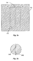
- FIG. 1 is an exploded view of a millimeter wave radar system including a plurality of channels formed in a metal backing plate and an adjacent microstrip antenna array assembly according to the present invention
- FIG. 2 a is a bottom plan view of a ground plane included in the microstrip antenna array assembly illustrated in FIG. 1;
- FIG. 2 b is a detailed view of the ground plane illustrated in FIG. 2 a;
- FIG. 3 a is a top plan view of a microstrip antenna array included in the microstrip antenna array assembly illustrated in FIG. 1;
- FIG. 3 b is a detailed view of the microstrip antenna array illustrated in FIG. 3 a.
- a millimeter wave radar system that can be employed in automotive Adaptive Cruise Control (ACC) applications is disclosed.
- the millimeter wave radar system includes a single microstrip antenna array that uses capacitive stub matching at waveguide-slot-microstrip transitions to cancel out a net inductive reactance at the transitions, thereby reducing return loss at microstrip antenna ports to enhance the performance of the overall system.
- FIG. 1 depicts an illustrative embodiment of a millimeter wave radar system 100 in accordance with the present invention.
- the millimeter wave radar system 100 includes a plurality of channels 108 formed in a metal backing plate 102 ; and, a microstrip antenna array assembly comprising a single microstrip antenna array 112 (also known as a patch antenna array) disposed on a surface of a substantially planar circuit board 106 , and an adjacent ground plane 104 .
- a microstrip antenna array assembly comprising a single microstrip antenna array 112 (also known as a patch antenna array) disposed on a surface of a substantially planar circuit board 106 , and an adjacent ground plane 104 .
- the microstrip antenna array 112 includes a plurality of conductive microstrips shown generally at reference numeral 114 , pluralities of rectangular open circuit tuning stubs shown generally at reference numeral 116 and positioned at regular intervals on the respective conductive microstrips 114 , and pluralities of radiating antenna elements such as square antenna element 115 coupled to the respective conductive microstrips 114 .
- Each radiating antenna element 115 is coupled to one of the conductive microstrips 114 by a microstrip feed line (not numbered).
- the microstrip antenna array 112 comprising the conductive microstrips 114 , the open circuit tuning stubs 116 , and the square antenna elements 115 may be fabricated on the surface of the circuit board 106 by a conventional photo etching process or any other suitable process.
- a dielectric substrate (not numbered) of the circuit board 106 separates the plurality of conductive microstrips 114 from the adjacent ground plane 104 to form a corresponding plurality of microstrip transmission lines.
- the ground plane 104 is mounted to the metal backing plate 102 comprising the plurality of channels 108 to form a corresponding plurality of waveguides having generally rectangular cross-section.
- respective opposing surfaces of the ground plane 104 may be bonded to the dielectric substrate of the circuit board 106 and the metal backing plate 102 using an epoxy resin or any other suitable adhesive.
- the ground plane 104 has a plurality of slots 110 formed therethrough and arranged in three (3) columns, in which each column includes the same number of collinear slots. Further, each conductive microstrip 114 has three (3) open circuit tuning stubs 116 positioned thereon such that each rectangular stub 116 is in registration with a respective slot 110 .
- the plurality of slots 110 may be formed through the ground plane 104 by etching or any other suitable technique.
- each one of the waveguide-slot-microstrip transitions is configured to transfer electromagnetic wave energy between a respective microstrip transmission line and a respective waveguide.
- the plurality of waveguide-slot-microstrip transitions comprising the slots 110 is configured to transfer the respective waves to the single microstrip antenna array 112 to produce phase differences in the waves, thereby causing the transmission of three (3) directional beams by the radiating antenna elements 115 .
- FIG. 2 a depicts a bottom plan view of the ground plane 104 included in the millimeter wave radar system 100 (see FIG. 1 ).
- the plurality of slots 110 are formed through the ground plane 104 in three (3) columns, in which each column comprises thirty (30) collinear slots 110 .
- the ground plane 104 and the microstrip antenna array 112 are arranged in the microstrip antenna array assembly so that one (1) slot 110 from each column feeds an electromagnetic wave to a respective microstrip transmission line.
- FIG. 2 b depicts a detailed view of the ground plane 104 including illustrative embodiments of slots 110 a and 110 b.
- FIG. 3 a depicts a top plan view of the circuit board 106 included in the millimeter wave radar system 100 (see FIG. 1 ), in which a preferred embodiment of the microstrip antenna array 112 is shown.
- the microstrip antenna array 112 includes thirty (30) parallel conductive microstrips 114 . Further, each conductive microstrip 114 has three (3) open circuit tuning stubs 116 positioned at regular intervals thereon.
- each rectangular stub 116 is in registration with one of the slots 110 (see FIG. 1 ), and one (1) slot 110 from each of the three (3) columns of slots 110 feeds an electromagnetic wave from a waveguide to a respective microstrip transmission line of the microstrip antenna array assembly.
- phase differences are produced in the waves, which accumulate to cause the antenna elements 115 to transmit three (3) directional beams at predetermined angles.
- FIG. 3 b depicts a detailed view of the microstrip antenna array 112 including illustrative embodiments of conductive microstrips 114 a and 114 b .
- the conductive microstrip 114 a has an open circuit rectangular stub 116 a positioned thereon, and a plurality of antenna elements 115 a coupled thereto.
- the conductive microstrip 114 b has an open circuit rectangular stub 116 b positioned thereon, and a plurality of antenna elements 115 b coupled thereto.
- each of the rectangular stubs 116 a and 116 b is in registration with a respective slot 110 in the ground plane 104 (see FIG. 1 ).
- each of the open circuit stubs 116 such as the stubs 116 a and 116 b is configured to provide capacitive stub matching to compensate for the net inductance introduced by the waveguide-slot-microstrip transitions.
- return loss at the microstrip antenna ports is reduced, thereby allowing full illumination of the microstrip antenna array.
- the rectangular stubs 116 are adjusted to a predetermined length.
- the length of the rectangular stubs 116 is equidistant about the respective conductive microstrips 114 .
- the stub length is preferably less than one quarter of a wavelength at the operating frequency of the system, which is preferably about 77 GHz.
- the rectangular stubs 116 are positioned on the respective conductive microstrips 114 so that each stub 116 is in registration with a respective slot 110 in the ground plane 104 .
- the length of the slots 110 is less than one half of a wavelength at the operating frequency of 77 GHz, and the slot width is narrow relative to the wavelength.
- the length of the rectangular stubs 116 is adjusted relative to the length of the slots 110 .
- the stub lengths are adjusted to provide an impedance of about 50 ⁇ at the waveguide-slot-microstrip transitions.
- the millimeter wave radar system 100 of FIG. 1 can be used to implement ACC systems in automotive vehicles.
- the millimeter wave radar system 100 may be mounted on an automotive vehicle (not shown), and the microstrip antenna array 112 may be configured to transmit directional beams to scan a field of view in a roadway ahead of the vehicle and collect information about objects within the field of view.
- the collected information may include data on the speed, direction, and/or distance of the objects in the roadway relative to the vehicle.
- the ACC system may subsequently use that information to decide, e.g., whether to alert a driver of the vehicle to a particular obstacle in the roadway and/or automatically change the speed of the vehicle to prevent a collision with the obstacle.
- the illumination of a vertical plane of the microstrip antenna array 112 in an ACC application can be improved.
- the microstrip antenna array assembly including the single microstrip antenna array 112 comprising the impedance matching stubs 116 , and the ground plane 104 comprising the three (3) columns of collinear slots 110 (see FIG. 1 ), may be used to implement a three-beam automotive antenna.
- the illustrated embodiment of the millimeter wave radar system 100 includes the rectangular open circuit stubs 116 (see FIGS. 3 a and 3 b ), the system 100 may alternatively include tuning stubs shaped as squares, fans, arcs, or any other geometrical shape suitable for providing capacitive stub matching.
- the geometrical shape of the radiating antenna elements 115 may take different forms.
- the electrical parameters of the dielectric substrate, the dimensions of the conductive microstrips 114 , the dimensions of the microstrip feed lines, the dimensions of the radiating antenna elements 115 , and the size and position of the slots 110 may be modified for further enhancing the performance of the system.
Landscapes
- Waveguide Aerials (AREA)
- Radar Systems Or Details Thereof (AREA)
Abstract
Description
Claims (16)
Priority Applications (1)
| Application Number | Priority Date | Filing Date | Title |
|---|---|---|---|
| US09/905,245 US6509874B1 (en) | 2001-07-13 | 2001-07-13 | Reactive matching for waveguide-slot-microstrip transitions |
Applications Claiming Priority (1)
| Application Number | Priority Date | Filing Date | Title |
|---|---|---|---|
| US09/905,245 US6509874B1 (en) | 2001-07-13 | 2001-07-13 | Reactive matching for waveguide-slot-microstrip transitions |
Publications (2)
| Publication Number | Publication Date |
|---|---|
| US20030011517A1 US20030011517A1 (en) | 2003-01-16 |
| US6509874B1 true US6509874B1 (en) | 2003-01-21 |
Family
ID=25420486
Family Applications (1)
| Application Number | Title | Priority Date | Filing Date |
|---|---|---|---|
| US09/905,245 Expired - Lifetime US6509874B1 (en) | 2001-07-13 | 2001-07-13 | Reactive matching for waveguide-slot-microstrip transitions |
Country Status (1)
| Country | Link |
|---|---|
| US (1) | US6509874B1 (en) |
Cited By (6)
| Publication number | Priority date | Publication date | Assignee | Title |
|---|---|---|---|---|
| US6642890B1 (en) * | 2002-07-19 | 2003-11-04 | Paratek Microwave Inc. | Apparatus for coupling electromagnetic signals |
| US20040263277A1 (en) * | 2003-06-30 | 2004-12-30 | Xueru Ding | Apparatus for signal transitioning from a device to a waveguide |
| FR2893451A1 (en) * | 2005-11-14 | 2007-05-18 | Bouygues Telecom Sa | DIRECT ACCESS FLAT ANTENNA SYSTEM IN WAVEGUIDE. |
| US8063832B1 (en) * | 2008-04-14 | 2011-11-22 | University Of South Florida | Dual-feed series microstrip patch array |
| CN105811113A (en) * | 2016-05-05 | 2016-07-27 | 桂林电子科技大学 | K-wave band microstrip patch antenna array |
| CN106129607A (en) * | 2016-07-19 | 2016-11-16 | 湖北三江航天红林探控有限公司 | Millimeter Wave Fuze Antenna |
Families Citing this family (9)
| Publication number | Priority date | Publication date | Assignee | Title |
|---|---|---|---|---|
| US6999039B2 (en) * | 2004-07-04 | 2006-02-14 | Victory Microwave Corporation | Extruded slot antenna array and method of manufacture |
| US7420436B2 (en) * | 2006-03-14 | 2008-09-02 | Northrop Grumman Corporation | Transmission line to waveguide transition having a widened transmission with a window at the widened end |
| US10490905B2 (en) * | 2016-07-11 | 2019-11-26 | Waymo Llc | Radar antenna array with parasitic elements excited by surface waves |
| US10673147B2 (en) | 2016-11-03 | 2020-06-02 | Kymeta Corporation | Directional coupler feed for flat panel antennas |
| KR102599824B1 (en) * | 2016-12-29 | 2023-11-07 | 라드시 테크놀로지즈 엘티디 | antenna array |
| CN110456313A (en) * | 2019-08-27 | 2019-11-15 | 青岛若愚科技有限公司 | Device applied to rectangular microstrip millimetre-wave radar sensor |
| CN110931968B (en) * | 2019-11-28 | 2025-03-25 | 广东盛路通信科技股份有限公司 | A millimeter-wave microstrip planar array antenna with low cross-polarization |
| CN111106441A (en) * | 2020-01-09 | 2020-05-05 | 西安理工大学 | Miniaturized directional radiation antenna based on artificial surface plasmon polariton |
| US11378683B2 (en) * | 2020-02-12 | 2022-07-05 | Veoneer Us, Inc. | Vehicle radar sensor assemblies |
Citations (9)
| Publication number | Priority date | Publication date | Assignee | Title |
|---|---|---|---|---|
| US5010351A (en) | 1990-02-08 | 1991-04-23 | Hughes Aircraft Company | Slot radiator assembly with vane tuning |
| US5990844A (en) * | 1997-06-13 | 1999-11-23 | Thomson-Csf | Radiating slot array antenna |
| US6127901A (en) | 1999-05-27 | 2000-10-03 | Hrl Laboratories, Llc | Method and apparatus for coupling a microstrip transmission line to a waveguide transmission line for microwave or millimeter-wave frequency range transmission |
| US6133877A (en) * | 1997-01-10 | 2000-10-17 | Telefonaktiebolaget Lm Ericsson | Microstrip distribution network device for antennas |
| US6144344A (en) * | 1997-12-10 | 2000-11-07 | Samsung Electronics Co., Ltd. | Antenna apparatus for base station |
| US6188361B1 (en) * | 1998-10-05 | 2001-02-13 | Alcatel | Active antenna panel of multilayer structure |
| US6313807B1 (en) * | 2000-10-19 | 2001-11-06 | Tyco Electronics Corporation | Slot fed switch beam patch antenna |
| US6377217B1 (en) * | 1999-09-14 | 2002-04-23 | Paratek Microwave, Inc. | Serially-fed phased array antennas with dielectric phase shifters |
| US6396440B1 (en) * | 1997-06-26 | 2002-05-28 | Nec Corporation | Phased array antenna apparatus |
-
2001
- 2001-07-13 US US09/905,245 patent/US6509874B1/en not_active Expired - Lifetime
Patent Citations (9)
| Publication number | Priority date | Publication date | Assignee | Title |
|---|---|---|---|---|
| US5010351A (en) | 1990-02-08 | 1991-04-23 | Hughes Aircraft Company | Slot radiator assembly with vane tuning |
| US6133877A (en) * | 1997-01-10 | 2000-10-17 | Telefonaktiebolaget Lm Ericsson | Microstrip distribution network device for antennas |
| US5990844A (en) * | 1997-06-13 | 1999-11-23 | Thomson-Csf | Radiating slot array antenna |
| US6396440B1 (en) * | 1997-06-26 | 2002-05-28 | Nec Corporation | Phased array antenna apparatus |
| US6144344A (en) * | 1997-12-10 | 2000-11-07 | Samsung Electronics Co., Ltd. | Antenna apparatus for base station |
| US6188361B1 (en) * | 1998-10-05 | 2001-02-13 | Alcatel | Active antenna panel of multilayer structure |
| US6127901A (en) | 1999-05-27 | 2000-10-03 | Hrl Laboratories, Llc | Method and apparatus for coupling a microstrip transmission line to a waveguide transmission line for microwave or millimeter-wave frequency range transmission |
| US6377217B1 (en) * | 1999-09-14 | 2002-04-23 | Paratek Microwave, Inc. | Serially-fed phased array antennas with dielectric phase shifters |
| US6313807B1 (en) * | 2000-10-19 | 2001-11-06 | Tyco Electronics Corporation | Slot fed switch beam patch antenna |
Cited By (11)
| Publication number | Priority date | Publication date | Assignee | Title |
|---|---|---|---|---|
| US6642890B1 (en) * | 2002-07-19 | 2003-11-04 | Paratek Microwave Inc. | Apparatus for coupling electromagnetic signals |
| US20040263277A1 (en) * | 2003-06-30 | 2004-12-30 | Xueru Ding | Apparatus for signal transitioning from a device to a waveguide |
| US7068121B2 (en) | 2003-06-30 | 2006-06-27 | Tyco Technology Resources | Apparatus for signal transitioning from a device to a waveguide |
| FR2893451A1 (en) * | 2005-11-14 | 2007-05-18 | Bouygues Telecom Sa | DIRECT ACCESS FLAT ANTENNA SYSTEM IN WAVEGUIDE. |
| WO2007054582A1 (en) * | 2005-11-14 | 2007-05-18 | Bouygues Telecom | Flat antenna system with a direct waveguide access |
| US20090096692A1 (en) * | 2005-11-14 | 2009-04-16 | Eduardo Motta Cruz | Flat Antenna System With a Direct Waveguide Access |
| CN101310413B (en) * | 2005-11-14 | 2012-11-28 | 布盖斯电信公司 | Flat antenna system with a direct waveguide access |
| US8063832B1 (en) * | 2008-04-14 | 2011-11-22 | University Of South Florida | Dual-feed series microstrip patch array |
| CN105811113A (en) * | 2016-05-05 | 2016-07-27 | 桂林电子科技大学 | K-wave band microstrip patch antenna array |
| CN106129607A (en) * | 2016-07-19 | 2016-11-16 | 湖北三江航天红林探控有限公司 | Millimeter Wave Fuze Antenna |
| CN106129607B (en) * | 2016-07-19 | 2019-10-18 | 湖北三江航天红林探控有限公司 | Millimeter Wave Fuze Antenna |
Also Published As
| Publication number | Publication date |
|---|---|
| US20030011517A1 (en) | 2003-01-16 |
Similar Documents
| Publication | Publication Date | Title |
|---|---|---|
| US6509874B1 (en) | Reactive matching for waveguide-slot-microstrip transitions | |
| US10615852B2 (en) | Multi beam former | |
| AU2002334695B2 (en) | Slot coupled, polarized radiator | |
| US6822615B2 (en) | Wideband 2-D electronically scanned array with compact CTS feed and MEMS phase shifters | |
| KR101621480B1 (en) | Transit structure of waveguide and dielectric waveguide | |
| EP2551959B1 (en) | Wide-band linked-ring antenna element for phased arrays | |
| US20030164797A1 (en) | Tunable multi-band antenna array | |
| EP1158602A1 (en) | Two-frequency antenna, multiple-frequency antenna, two- or multiple-frequency antenna array | |
| KR20150059392A (en) | Microstripline-fed slot array antenna and manufacturing method thereof | |
| US6452550B1 (en) | Reduction of the effects of process misalignment in millimeter wave antennas | |
| US11223112B2 (en) | Inverted microstrip travelling wave patch array antenna system | |
| US11515624B2 (en) | Integrated cavity backed slot array antenna system | |
| WO2020177713A1 (en) | Dual-polarized substrate-integrated beam steering antenna | |
| US9214729B2 (en) | Antenna and array antenna | |
| CN114336003B (en) | Antenna, preparation method thereof, millimeter wave sensor and terminal | |
| US12062863B2 (en) | Antenna device | |
| WO2001052352A1 (en) | Array antenna for d-shaped, h-plane radiation pattern | |
| EP1617513A1 (en) | Wideband omnidirectional radiating device | |
| CN219626892U (en) | Millimeter wave antenna, radar and automobile | |
| Kolak et al. | A low profile 77 GHz three beam antenna for automotive radar | |
| EP4205231B1 (en) | Conformal rf antenna array and integrated out-of-band eme rejection filter | |
| US6999030B1 (en) | Linear polarization planar microstrip antenna array with circular patch elements and co-planar annular sector parasitic strips | |
| WO2019189008A1 (en) | Antenna | |
| US20040113856A1 (en) | Antenna | |
| CN119315285A (en) | A double-ridged waveguide slot array antenna and vehicle-mounted millimeter wave radar device |
Legal Events
| Date | Code | Title | Description |
|---|---|---|---|
| AS | Assignment |
Owner name: TYCO ELECTRONICS CORPORATION, PENNSYLVANIA Free format text: ASSIGNMENT OF ASSIGNORS INTEREST;ASSIGNORS:KOLAK, FRANK;CHANNABASSAPPA, ESWARAPPA;REEL/FRAME:012156/0551 Effective date: 20010719 |
|
| STCF | Information on status: patent grant |
Free format text: PATENTED CASE |
|
| FPAY | Fee payment |
Year of fee payment: 4 |
|
| AS | Assignment |
Owner name: AUTOILV ASP, INC., UTAH Free format text: ASSIGNMENT OF ASSIGNORS INTEREST;ASSIGNORS:M/A-COM, INC.;TYCO ELECTRONICS TECHNOLOGY RESOURCES, INC.;TYCO ELECTRONICS CORPORATION;AND OTHERS;REEL/FRAME:021750/0045 Effective date: 20080926 Owner name: AUTOILV ASP, INC.,UTAH Free format text: ASSIGNMENT OF ASSIGNORS INTEREST;ASSIGNORS:M/A-COM, INC.;TYCO ELECTRONICS TECHNOLOGY RESOURCES, INC.;TYCO ELECTRONICS CORPORATION;AND OTHERS;REEL/FRAME:021750/0045 Effective date: 20080926 |
|
| FPAY | Fee payment |
Year of fee payment: 8 |
|
| FPAY | Fee payment |
Year of fee payment: 12 |
|
| AS | Assignment |
Owner name: VEONEER US, INC., MICHIGAN Free format text: ASSIGNMENT OF ASSIGNORS INTEREST;ASSIGNOR:AUTOLIV ASP, INC.;REEL/FRAME:046326/0137 Effective date: 20180608 |
|
| AS | Assignment |
Owner name: VEONEER US, LLC, DELAWARE Free format text: CHANGE OF NAME;ASSIGNOR:VEONEER US, INC.;REEL/FRAME:061069/0535 Effective date: 20220401 |
|
| AS | Assignment |
Owner name: VEONEER US, LLC, MICHIGAN Free format text: AFFIDAVIT / CHANGE OF ADDRESS;ASSIGNOR:VEONEER US, LLC;REEL/FRAME:065049/0150 Effective date: 20220426 |