US6505316B1 - Peripheral partitioning and tree decomposition for partial scan - Google Patents
Peripheral partitioning and tree decomposition for partial scan Download PDFInfo
- Publication number
- US6505316B1 US6505316B1 US09/497,521 US49752100A US6505316B1 US 6505316 B1 US6505316 B1 US 6505316B1 US 49752100 A US49752100 A US 49752100A US 6505316 B1 US6505316 B1 US 6505316B1
- Authority
- US
- United States
- Prior art keywords
- vertex
- cost
- graph
- scan
- degree
- Prior art date
- Legal status (The legal status is an assumption and is not a legal conclusion. Google has not performed a legal analysis and makes no representation as to the accuracy of the status listed.)
- Expired - Lifetime
Links
Images


Classifications
-
- G—PHYSICS
- G01—MEASURING; TESTING
- G01R—MEASURING ELECTRIC VARIABLES; MEASURING MAGNETIC VARIABLES
- G01R31/00—Arrangements for testing electric properties; Arrangements for locating electric faults; Arrangements for electrical testing characterised by what is being tested not provided for elsewhere
- G01R31/28—Testing of electronic circuits, e.g. by signal tracer
- G01R31/317—Testing of digital circuits
- G01R31/3181—Functional testing
- G01R31/3185—Reconfiguring for testing, e.g. LSSD, partitioning
- G01R31/318533—Reconfiguring for testing, e.g. LSSD, partitioning using scanning techniques, e.g. LSSD, Boundary Scan, JTAG
- G01R31/318583—Design for test
- G01R31/318586—Design for test with partial scan or non-scannable parts
Definitions
- the invention relates to scan techniques for sequential circuits.
- this invention relates to new partial scan techniques using peripheral partitioning and tree decomposition.
- the invention is embodied in a system to perform partial scan using peripheral partitioning and tree decomposition, in a method for partial scan using peripheral partitioning, in a method for partial scan using tree decomposition, and in a computer program product for enabling a computer to operate according to the method.
- testability techniques such as scan have been used widely for achieving high test coverage for sequential circuits.
- memory elements including flip-flops
- a full scan involves the chaining of all the shift registers in the circuit to be tested.
- Scan provides for direct controllability and observability of all memory elements during the test mode.
- area and performance penalties of full scan design are unacceptable for many sequential circuit designs.
- Partial scan techniques involve selecting only a subset of memory elements. This reduces area and performance penalties involved in a full scan.
- Testability analysis based approach is one of the approaches that is known in the prior art. See E. Trischler, “Incomplete Scan Path with an Automatic Test Generation Methodology,” in Proceedings of the international Test Conference, pp. 153-162, 1980; M. Abramovici, J. J. Kulikowski, and R. K. Roy, “The Best Flip-Flops to Scan,” in Proceedings of the International Test Conference, pp. 166-173, 1991; K. S. Kim and C. R. Kime, “Partial Scan by Use of Empirical Testability,” in Proceedings of the International Conference on Computer-Aided Design, pp. 314-317, November 1990; P. S. Parikh and M.
- testability analysis based methods use cost metrics during scan selection.
- the ability of testability based approaches to tightly correlate with sequential test generation effort required for large designs is not clearly established. Further, one often has to rely on the test generator to refine the measures and/or to gain confidence on the scan selection based on these testability measures. Some of the more sophisticated testability measures require large computational resources.
- Test generation based approaches select scan memory elements based on identification of hard-to-detect faults. This approach is tightly coupled with the test generation tool and does not offer the designer any flexibility to determine scan flip-flops a priori. Further, scan selection strongly depends on the order of faults chosen by the test generation.
- Structural partial scan methods analyze the structure of the flip-flop dependency graph and base their scan selection on structural properties of this graph. Most of the structural methods have centered around breaking feedback loops, a technique first introduced by Cheng et al. See Cheng and V. D. Agrawal, “A Partial Scan Method for Sequential Circuits with Feedback,” IEEE Transactions on Computers, vol. 39, pp. 544-548, April 1990. This approach called self-loop acyclic all feedback loops except self-loops are broken. A self-loop here refers to a situation where the output of a flip-flop, after passing through combinational logic, feeds back into the same flip-flop. This approach results in low area overhead, however, it is not effective for test generation.
- FIG. 13 depicts a table showing area overhead and test generation results for the larger benchmark circuits. The data shows that self-loop acyclic technique entails low area overhead but the scanned circuits are hard to test. Pipeline method produces circuits that are easy to test but this method entails high area overhead.
- an objective of this invention is to provide a method of performing partial scan of a sequential circuit using peripheral partitioning.
- Yet another objective of this invention is to provide a method for partitioning a sequential circuit into peripheral partitions.
- Yet another objective of this invention is to provide a method to solve the cycle cut-set problem, associated with peripheral partitioning.
- Yet another objective of this invention is to provide a method for tree decomposition of an undirected graph, representing a sequential circuit, into trees.
- Yet another objective of this invention is to provide a system that uses peripheral partitioning method and the tree decomposition method of the current invention to form a partial scanned circuit.
- Yet another objective of this invention is to provide a program product that enables a computer to perform the peripheral partitioning method and the tree decomposition method of the current invention to form partial scanned circuit.
- a partial scan system for sequential circuits comprising an input unit, a peripheral partitioning unit, a tree decomposition unit, a circuit redesign unit and an output unit.
- Another embodiment of the present invention is a system and method of partial scan for a sequential circuit using peripheral partitioning.
- This invention also includes a system and method of partial scan for a sequential circuit using tree decomposition.
- Another embodiment of this invention is a system and method of peripheral partitioning a sequential circuit to form a plurality of partitions, wherein each of said plurality of partitions comprise a group of memory elements, each memory element in said group of memory element do not form a combination path with memory elements not belonging to said group of memory elements.
- Another embodiment of this invention is a method of peripheral partitioning a sequential circuit comprising: drawing an S-graph of the sequential circuit; remodeling the S-graph into a new undirected graph; eliminating cycles in the new undirected graph by selecting a minimal set of vertices.
- Another embodiment of this invention is a method of selecting a minimal set of vertices to break all cycles comprising computing bi-connected components to form a plurality of bi-connected components; adding one vertex from each of said plurality of bi-connected components to a cycle cut-set; removing said one vertex from each of said plurality of biconnected components; and repeating the steps until there are no more bi-connected components.
- Another embodiment of this invention is a computer program product comprising, computer readable instructions, and a computer readable medium bearing said computer readable instructions; said instructions being adaptable to enable a computer to operate according to the steps of: receiving a sequential circuit from the user; tree decompositioning the circuit for a partial scan; returning the partial scan circuit to the user.
- Another embodiment of this invention is a computer program product comprising, computer readable instructions and a computer medium bearing said computer readable instructions; said instructions being adaptable to enable a computer to operate according to the steps of: receiving a sequential circuit from the user; peripheral partitioning the circuit to form a partial scanned circuit; checking if tree decompositioning can be performed on this partial scanned circuit; tree decompositioning the circuit if tree decompositioning can be performed on the circuit to form a refined partial scanned circuit; returning the refined partial scanned circuit to the user.
- FIG. 1 is a partial scan system according to the present invention.
- FIG. 2 is a partial scan system that performs peripheral partitioning and tree decompositioning according to the present invention.
- FIG. 3 is a partial scan system that solves the cycle cut set problem according to the present invention.
- FIG. 4 represents a sequential circuit in the form of peripherally interacting partitions.
- FIG. 5 provides an example of a S-graph.
- FIG. 6 depicts the peripheral partitions of the example S-graph provided in FIG. 5 .
- FIG. 7 depicts a remodelled S-graph of the sequential circuit provided in FIG. 5 in the form of a undirected graph.
- FIG. 8 shows the tree decomposition partitioning of the undirected S-graph.
- FIG. 9 is a flowchart showing the steps in performing the peripheral partitioning of a sequential circuit according to the present invention.
- FIG. 10 shows a undirected S-graph after one iteration.
- FIG. 11 shows a cost model for tree decomposition heuristic.
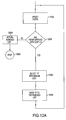
- FIG. 12A is a flowchart showing the steps in performing tree decompositioning of a sequential circuit according to the present invention.
- FIG. 12B is a flowchart showing the steps in updating cost for the tree decompositioning of a sequential circuit according to the present invention
- FIGS. 13-17 show tables illustrating the results of experiments conducted using the ISCAS 89 sequential benchmark circuits.
- a key component of this invention is the selection of scan flip-flops so that the circuit satisfies two key properties in the test mode.
- the circuit is partitioned into peripherally interacting finite state machines (peripheral partitions). Peripheral partitions do not have combinational paths between flip-flops belonging to different partitions.
- Another aspect of this invention is that the flip-flop dependency graph (S-graph) of a sequential circuit is decomposed into peripheral partitions that have a tree structures. It is to be noted that both peripheral partitioning and tree decomposition should be used in combination for best results.
- S-graph captures dependencies among flip-flops by including an arc from flip-flop F 1 to flip-flop F 2 if there is a combinational path from F 1 to F 2 .
- This invention show that peripheral partitions with tree structure S-graphs inherently require low sequential test generation resources.
- a further aspect of this invention is to provide an efficient algorithm for peripheral partitioning and tree decomposition.
- the scan flip-flop selection algorithm iteratively partitions the S-graph into several disjoint sub-graphs that have special structures. This invention examines sub-graphs that are trees.
- Peripheral partitioning and tree decomposition do not require breaking of self-loops. This is advantageous since most of the flip-flops in industrial designs have self-loops.
- FIG. 1 depicts a partial scan system according to the present invention.
- a sequential circuit description is input to the system.
- the sequential circuit is partial scanned according to the present invention.
- the partial scanned circuit is returned to the user.
- FIG. 2 depicts a more detailed description of the present invention.
- the sequential circuit description is peripherally partitioned according to the present invention.
- a tree composition is performed on the resulting sequential circuit.
- S-graph The structural dependencies among flip-flops can be represented by a directed graph, called the S-graph. See D. Lee and S. Reddy, “On Determining Scan Flip-Flops in Partial-Scan Designs,” in Proceedings of the International Conference on Computer - Aided Design, pp. 322-325, November 1990.
- S-graph has a vertex for every flip-flop in the circuit. There exists an arc from vertex v i to vertex v j if there is a combinational path from flip-flop v i to flip-flop v j . Also, there is an arc from vertex v i to itself (self-loop) if there is a combinational path from flip-flop v i to itself.
- FIG. 3 a more detailed representation of the peripheral partition using S-graphs is presented.
- an S-graph for a sequential circuit is generated.
- the S-graph is then input to block 320 where the graph is remodeled to produce a new undirected graph.
- vertices are selected and removed so that cycles in this S-graph are eliminated.
- the removed vertices are included in a scan chain partial scanned sequential circuit.
- Circles labeled as C are combinational logic blocks that are shared among several finite state machines (partitions) represented by rectangular boxes that are labeled as P (blocks 430 - 432 ).
- component finite state machines can be of arbitrary complexity but there are no combinational paths between flip-flops of different partitions. In particular, component machines can have feedback paths involving an arbitrary number of flip-flops.
- component state machines share only primary inputs, primary outputs and combinational logic blocks. Therefore, outputs of a partition cannot drive the inputs of another partition.
- the next state of a partition is determined only by the present state of flip-flops in the partition. In particular, the next state does not depend on the present state of flip-flops in other partitions.
- Peripheral partitions can be identified by constructing the S-graph. If the vertices of the S-graph can be partitioned such that arcs exist only between vertices in the same partition, then the S-graph naturally has peripheral partitions. If the S-graph does not have peripheral partitions, then one can identify scan flip-flops to induce peripheral partitions in the test mode.
- This graph corresponds to a circuit with 18 flip-flops. Note that every flip-flop has a self-loop and the circuit has feedback cycles that include more than one flip-flop.
- This S-graph has no peripheral partitions. This is because it is impossible to partition the vertices into disjoint sets so that arcs exist only between vertices of the same partition.
- flip-flops 7 , 9 and 12 are selected for partial scan, then the S-graph in the test mode is as shown in FIG. 6 .
- This graph has three peripheral partitions: ⁇ 1 , 2 , 3 , 4 , 5 , 6 , 8 ⁇ , ⁇ 10 , 11 , 14 , 15 , 17 ⁇ , and ⁇ 13 , 16 , 18 ⁇ .
- Sangiovanni-Vincentelli “A Synthesis and Optimization Procedure for Fully and Easily Testable Sequential Machines,” IEEE Transactions on Computer Aided Design, vol. 8, pp. 1100-1107, October 1989; A. Ghosh, S. Devadas, and A. R. Newton, Sequential Logic Testing and Verification. Kluwer Academic Publishers, Boston, 1992; and X. Chen and M. L. Bushnell, “Dynamic State and Objective Learning for Sequential Circuit Automatic Test Generation Using Decomposition Equivalence,” in Proceedings of the 24 th IEEE International Symposium on Fault Tolerant Computing, pp. 446-455, June 1994.
- Peripheral partitions are particularly attractive since initialization of flip-flops in a partition can be performed independent of flip-flops in other partitions.
- a tree decomposition has two desirable properties. First, there is no sequential re-convergence if we ignore the self-loops. For example, consider the S-graph of FIG. 5 . The sub-graph consisting of vertices 6 , 8 and 9 forms a sequential re-convergence for flip-flop 6 . However, after selecting three flip-flops for scan, this S-graph is partitioned into a tree decomposition. Absence of sequential re-convergence eliminates signal correlations across multiple time frames. This could potentially lead to a reduction in sequential test generation effort. Second, initialization of flip-flops in a tree decomposition can be performed in a levelized order. Consider the peripheral partition ⁇ 1 , 2 , 3 , 4 , 5 , 6 , 7 ⁇ shown in FIG. 6 . Since the sub-graph is a tree, it is possible to assign level numbers to the vertices.
- Roots are assigned a level of 0. Every other vertex is assigned a level that is one more than the maximum level of any of its immediate predecessors.
- Flip-flop initialization can be performed level by level by first initializing flip-flops at leaf level and proceeding one level after another to the root.
- Scan flip-flops are selected to partition the S-graph into peripheral partitions with tree structures using a two-part procedure.
- the directed S-graph of FIG. 5 is remodelled into an undirected graph as shown in FIG. 4 (self-loop arcs are not shown). Note that the two-cycle with vertices 12 and 16 will reduce to a single edge since every arc is replaced by an edge.
- vertex 12 is split into 12 a and 12 b. All the incoming arcs of vertex 12 in FIG. 2 are now shown as edges incident to 12 a and all the outgoing arcs of vertex 12 are shown as edges incident to 12 b. An edge is also added between 12 a and 12 b.
- the two-cycle ⁇ 12 , 16 ⁇ has been expanded to the cycle ⁇ 12 a, 16 , 12 b ⁇ . A minimum set of vertices to break all cycles in the undirected model is selected.
- cycle cut set problem The problem of selecting a set of vertices in an undirected graph whose removal breaks all (undirected) cycles is referred to as the cycle cut set problem.
- the smallest such set called the minimum cycle cut set is to be found.
- This problem belongs to the class of NP-hard problems.
- An efficient heuristic to find a cycle cut set in the undirected model of the S-graph is another aspect of this invention. The following procedure computes a cycle cut set.
- Procedure Cycle Cut Set(S) do ⁇ compute biconnected components (BCC's); pick one vertex from each bcc and add to ccs_list; remove(v) for all vertices ‘v’ picked from the BCC's; ⁇ while (S has biconnected components) return(ccs_list);
- a biconnected component (BCC) of an undirected graph is a maximal set of edges such any two edges in the set lie on a common simple cycle. See T. H. Cormen, C. E. Leiserson, and R. L. Rivest. In other words for any two vertices in the biconnected component there exist two distinct vertex disjoint paths. It is to be noted that cycles and biconnected components are closely related. If a graph does not have cycles it will not have any biconnected components and vice-versa.
- At least one vertex from every BCC is selected.
- the vertex whose biconnected degree (the incident edges that belong to biconnected components) is the highest for that component is selected. Note that the edges incident to a vertex can belong to different biconnected components (and hence the vertex will belong to each of these bcc's) and the biconnected degree is sum of these edges.
- the S-graph will not have any biconnected components implying that all the cycles have been broken.
- Flip-flops corresponding to selected vertices are the scan flip-flops. If the scan flip-flops are removed from the S-graph, then the graph has no sequential reconvergence except through self-loops. However, vertices can have out-degree>1 and these sub-graphs may not satisfy a tree decomposition yet.
- FIG. 9 depicts a flowchart of the cycle cut-set problem according to the present invention.
- the sequential circuit graph is input to block 910 .
- Block 910 computes the biconnected components of the graph.
- the algorithm enters a loop.
- a decision is made whether there are any more BCC's to be processed. If there are no more BCC's to be processed the cut-set said list is returned in 960 . If there are more BCC's to be processed then the algorithm enters block 930 .
- one vertex is selected from each BCC.
- the selected vertex is removed from the BCC.
- block 950 the removed vertex is added to the cut-set list and the algorithm returns to block 920 .
- the cut-set list is returned to the user in block 960 .
- An important aspect of this invention is a scan selection procedure that identifies vertices that have to be removed to satisfy the tree decomposition.
- Sub-graphs in a tree decomposition are trees with exactly one sink vertex.
- FIG. 12A represents a flowchart for tree decomposition.
- costs associated with all the vertices are updated using the algorithm represented by the flowchart shown in FIG. 12 B.
- block 1220 A a determination is made to see if there are any vertices with costs greater than zero. If there are vertices with costs greater than zero, the algorithm moves to block 1230 A where a vertex ‘v’ with the maximum cost is selected. This vertex ‘v’ is then moved to the “removed-list” in block 1240 A. The algorithm then returns to block 1210 A and the processing is continued. If there are no vertices with costs greater than zero in block 1220 A, the algorithm moves to block 1250 A where all the vertices in the “removed-list” are returned. The algorithm finally stops in 1260 A.
- FIG. 12B Flowchart shown in FIG. 12B represents the algorithm used for updating costs.
- the costs associated with each vertex is initialized to zero.
- the out-degrees for all vertices are computed.
- all the in-degree vertices for all vertices are identified.
- the algorithm enters a loop. If there are any more vertices left to update costs, the algorithm proceeds to block 1280 B where it returns back to algorithm in FIG. 12 A.
- a vertex ‘v’ is selected.
- a determination is made whether the out-degree for ‘v’ is greater than 1.
- step 1260 B a determination is made to see if there are more in-degree vertices for ‘v’ to be processed. If there are more in-degree vertices, a vertex ‘w’ which is an in-degree vertex of ‘v’ is selected in 1261 B. In block 1270 B a determination is made if out-degree for ‘w’ is greater than 1.
- the scan flip-flop selection technique according to the invention is preferably implemented in a C language program.
- FIG. 14 depicts a table showing the area overhead incurred by several partial scan proposals including the present technique.
- the area overhead figures for the proposed technique are compared with two other prior art techniques: one that selects flip-flops to break all feedback cycles except self-loops (self-loop acyclic) and one that selects flip-flops to break all feedback cycles including self-loops (pipeline).
- self-loop acyclic self-loop acyclic
- pipeline self-loops
- the first set SD 1 is obtained by using both peripheral partitioning and tree decomposition.
- the second set SD 2 is obtained by using only peripheral partitioning.
- Scan selection for the set SD 1 not only include all scan flip-flops in the set SD 2 , but may have additional scan flip-flops. Therefore, scan circuits of the set SD 2 have a lower scan overhead than the scan circuits of set SD 1 .
- the overhead figures for both SD 1 and SD 2 scan circuits are significantly lower when compared with the pipeline case.
- This preferred embodiment entails scanning about 20-40% of flip-flops in the larger designs as compared to the pipeline case that may require as high as 75% or more.
- the present invention has higher area overhead.
- high fault efficiencies are not achievable for the self-loop acyclic case.
- the CPU seconds required for selecting scan flip-flops is quite low even for the large circuits.
- FIG. 14 depicts a table showing test generation results for the pipeline case. High fault efficiencies are achieved for all circuits, including the larger ones, with very short CPU times.
- Column TAT shows the normalized test application time, as compared to the test application time required for circuits in the SD 1 set.
- Test generation results for the SD 1 and SD 2 cases are shown in tables shown in FIGS. 15 and 16, respectively.
- Max P The maximum number of flip-flops in any partition
- Max D maximum sequential depth for any partition
- Max T the maximum number of vectors in a test sequence for any fault
- test application times for the both these case are also lower than the pipeline case. Further, the test application time for the SD 2 case is typically lower than the SD 1 case.
- the current invention is also compared to a circuit partitioning technique suggested by T. Ono et al. See the present technique incurs lower area overhead and achieves significantly higher fault efficiencies with lower CPU resources. For example, consider the circuit S 13207 . The present invention selects only 142 flip-flops (SD 2 case). 99% fault efficiency is achieved in only 508 CPU seconds. In comparison, the prior art technique selects 217 flip-flops and achieves a fault efficiency of only 60.8% in about 7564 CPU seconds. The improvement in area overhead, fault efficiency and test generation CPU times is more pronounced for larger circuits.
Landscapes
- Engineering & Computer Science (AREA)
- General Engineering & Computer Science (AREA)
- Physics & Mathematics (AREA)
- General Physics & Mathematics (AREA)
- Tests Of Electronic Circuits (AREA)
- Test And Diagnosis Of Digital Computers (AREA)
Abstract
Description
| Procedure Cycle Cut Set(S) | ||
| do { | ||
| compute biconnected components (BCC's); | ||
| pick one vertex from each bcc and add to ccs_list; | ||
| remove(v) for all vertices ‘v’ picked from the BCC's; | ||
| } while (S has biconnected components) | ||
| return(ccs_list); | ||
| Procedure Out-degree Cut Set(S) | ||
| initialize cost(v) = 0; | ||
| for each vertex ‘v’ { | ||
| if (out-degree(v) > 1); | ||
| cost(v) = out-degree(v) − 1; | ||
| for each in-degree vertex ‘w’ { | ||
| if (out-degree(w) > 1); | ||
| cost(v) = cost(v) + 1; | ||
| } | ||
| } | ||
| while (costs > 0) { | ||
| pick ‘v’ with max cost and remove(v); | ||
| update costs; | ||
| } | ||
| return(vertices picked); | ||
Claims (5)
Priority Applications (1)
| Application Number | Priority Date | Filing Date | Title |
|---|---|---|---|
| US09/497,521 US6505316B1 (en) | 1997-12-19 | 2000-02-04 | Peripheral partitioning and tree decomposition for partial scan |
Applications Claiming Priority (2)
| Application Number | Priority Date | Filing Date | Title |
|---|---|---|---|
| US08/994,430 US6134687A (en) | 1997-12-19 | 1997-12-19 | Peripheral partitioning and tree decomposition for partial scan |
| US09/497,521 US6505316B1 (en) | 1997-12-19 | 2000-02-04 | Peripheral partitioning and tree decomposition for partial scan |
Related Parent Applications (1)
| Application Number | Title | Priority Date | Filing Date |
|---|---|---|---|
| US08/994,430 Division US6134687A (en) | 1997-12-19 | 1997-12-19 | Peripheral partitioning and tree decomposition for partial scan |
Publications (1)
| Publication Number | Publication Date |
|---|---|
| US6505316B1 true US6505316B1 (en) | 2003-01-07 |
Family
ID=25540664
Family Applications (3)
| Application Number | Title | Priority Date | Filing Date |
|---|---|---|---|
| US08/994,430 Expired - Lifetime US6134687A (en) | 1997-12-19 | 1997-12-19 | Peripheral partitioning and tree decomposition for partial scan |
| US09/497,521 Expired - Lifetime US6505316B1 (en) | 1997-12-19 | 2000-02-04 | Peripheral partitioning and tree decomposition for partial scan |
| US09/568,049 Expired - Lifetime US6732310B1 (en) | 1997-12-19 | 2000-05-10 | Peripheral partitioning and tree decomposition for partial scan |
Family Applications Before (1)
| Application Number | Title | Priority Date | Filing Date |
|---|---|---|---|
| US08/994,430 Expired - Lifetime US6134687A (en) | 1997-12-19 | 1997-12-19 | Peripheral partitioning and tree decomposition for partial scan |
Family Applications After (1)
| Application Number | Title | Priority Date | Filing Date |
|---|---|---|---|
| US09/568,049 Expired - Lifetime US6732310B1 (en) | 1997-12-19 | 2000-05-10 | Peripheral partitioning and tree decomposition for partial scan |
Country Status (1)
| Country | Link |
|---|---|
| US (3) | US6134687A (en) |
Cited By (1)
| Publication number | Priority date | Publication date | Assignee | Title |
|---|---|---|---|---|
| US20050228616A1 (en) * | 2004-04-09 | 2005-10-13 | Incentia Design Systems, Corp. | Method and system for providing fast design for testability prototyping in integrated circuit designs |
Families Citing this family (8)
| Publication number | Priority date | Publication date | Assignee | Title |
|---|---|---|---|---|
| US6622290B1 (en) * | 2000-10-03 | 2003-09-16 | Cadence Design Systems, Inc. | Timing verification method employing dynamic abstraction in core/shell partitioning |
| US6748564B1 (en) * | 2000-10-24 | 2004-06-08 | Nptest, Llc | Scan stream sequencing for testing integrated circuits |
| US8020122B2 (en) * | 2005-06-07 | 2011-09-13 | The Regents Of The University Of California | Circuit splitting in analysis of circuits at transistor level |
| US8423843B2 (en) * | 2009-10-23 | 2013-04-16 | Atrenta, Inc. | Method and system thereof for optimization of power consumption of scan chains of an integrated circuit for test |
| JP5327634B2 (en) * | 2009-11-02 | 2013-10-30 | 株式会社リコー | Rotation measuring device, sheet conveying device, document reading device, and image forming device |
| US10372855B2 (en) * | 2014-02-28 | 2019-08-06 | Mentor Graphics Corporation | Scan cell selection for partial scan designs |
| CN109581207B (en) * | 2018-12-19 | 2020-12-11 | 天津大学 | A Low-Cost Circuit State Control Method for Hardware Simulation of Fault Injection Attacks |
| CN109581206B (en) * | 2018-12-19 | 2020-12-11 | 天津大学 | A simulation method of integrated circuit fault injection attack based on partial scan |
Citations (13)
| Publication number | Priority date | Publication date | Assignee | Title |
|---|---|---|---|---|
| JPH03233A (en) | 1989-02-23 | 1991-01-07 | Bayerische Motoren Werke Ag | Lamellar structure for manufacturing sound insulating substance and sound insulating substance, and manufacture of lamellar structure and sound substance |
| US5043986A (en) | 1989-05-18 | 1991-08-27 | At&T Bell Laboratories | Method and integrated circuit adapted for partial scan testability |
| JPH05210497A (en) | 1992-01-31 | 1993-08-20 | Sega Enterp Ltd | Cd-rom disk and security check method for the disk |
| JPH0646179A (en) | 1992-07-23 | 1994-02-18 | Ricoh Co Ltd | Facsimile equipment |
| US5329533A (en) | 1991-12-26 | 1994-07-12 | At&T Bell Laboratories | Partial-scan built-in self-test technique |
| JPH0785060A (en) | 1993-09-13 | 1995-03-31 | Matsushita Electric Ind Co Ltd | Language converter |
| JPH07234784A (en) | 1994-02-22 | 1995-09-05 | Sega Enterp Ltd | Program execution device |
| US5461573A (en) * | 1993-09-20 | 1995-10-24 | Nec Usa, Inc. | VLSI circuits designed for testability and methods for producing them |
| US5502646A (en) * | 1993-12-02 | 1996-03-26 | Nec Usa, Inc. | Selection of partial scan flip-flops to break feedback cycles |
| US5513123A (en) * | 1994-06-30 | 1996-04-30 | Nec Usa, Inc. | Non-scan design-for-testability of RT-level data paths |
| US5731983A (en) * | 1995-12-29 | 1998-03-24 | Nec Usa, Inc. | Method for synthesizing a sequential circuit |
| US5802075A (en) * | 1997-01-16 | 1998-09-01 | Unisys Corporation | Distributed test pattern generation |
| JP3233051B2 (en) | 1996-12-20 | 2001-11-26 | 日本電気株式会社 | Method for manufacturing semiconductor device |
Family Cites Families (2)
| Publication number | Priority date | Publication date | Assignee | Title |
|---|---|---|---|---|
| TW253942B (en) * | 1994-01-31 | 1995-08-11 | At & T Corp | |
| CA2187466A1 (en) * | 1995-10-19 | 1997-04-20 | Kwang-Ting Cheng | Method for inserting test points for full- and partial-scan built-in self-testing |
-
1997
- 1997-12-19 US US08/994,430 patent/US6134687A/en not_active Expired - Lifetime
-
2000
- 2000-02-04 US US09/497,521 patent/US6505316B1/en not_active Expired - Lifetime
- 2000-05-10 US US09/568,049 patent/US6732310B1/en not_active Expired - Lifetime
Patent Citations (13)
| Publication number | Priority date | Publication date | Assignee | Title |
|---|---|---|---|---|
| JPH03233A (en) | 1989-02-23 | 1991-01-07 | Bayerische Motoren Werke Ag | Lamellar structure for manufacturing sound insulating substance and sound insulating substance, and manufacture of lamellar structure and sound substance |
| US5043986A (en) | 1989-05-18 | 1991-08-27 | At&T Bell Laboratories | Method and integrated circuit adapted for partial scan testability |
| US5329533A (en) | 1991-12-26 | 1994-07-12 | At&T Bell Laboratories | Partial-scan built-in self-test technique |
| JPH05210497A (en) | 1992-01-31 | 1993-08-20 | Sega Enterp Ltd | Cd-rom disk and security check method for the disk |
| JPH0646179A (en) | 1992-07-23 | 1994-02-18 | Ricoh Co Ltd | Facsimile equipment |
| JPH0785060A (en) | 1993-09-13 | 1995-03-31 | Matsushita Electric Ind Co Ltd | Language converter |
| US5461573A (en) * | 1993-09-20 | 1995-10-24 | Nec Usa, Inc. | VLSI circuits designed for testability and methods for producing them |
| US5502646A (en) * | 1993-12-02 | 1996-03-26 | Nec Usa, Inc. | Selection of partial scan flip-flops to break feedback cycles |
| JPH07234784A (en) | 1994-02-22 | 1995-09-05 | Sega Enterp Ltd | Program execution device |
| US5513123A (en) * | 1994-06-30 | 1996-04-30 | Nec Usa, Inc. | Non-scan design-for-testability of RT-level data paths |
| US5731983A (en) * | 1995-12-29 | 1998-03-24 | Nec Usa, Inc. | Method for synthesizing a sequential circuit |
| JP3233051B2 (en) | 1996-12-20 | 2001-11-26 | 日本電気株式会社 | Method for manufacturing semiconductor device |
| US5802075A (en) * | 1997-01-16 | 1998-09-01 | Unisys Corporation | Distributed test pattern generation |
Non-Patent Citations (27)
Cited By (2)
| Publication number | Priority date | Publication date | Assignee | Title |
|---|---|---|---|---|
| US20050228616A1 (en) * | 2004-04-09 | 2005-10-13 | Incentia Design Systems, Corp. | Method and system for providing fast design for testability prototyping in integrated circuit designs |
| US7134106B2 (en) * | 2004-04-09 | 2006-11-07 | Incentia Design Systems Corp. | Method and system for providing fast design for testability prototyping in integrated circuit designs |
Also Published As
| Publication number | Publication date |
|---|---|
| US6134687A (en) | 2000-10-17 |
| US6732310B1 (en) | 2004-05-04 |
Similar Documents
| Publication | Publication Date | Title |
|---|---|---|
| Kunz et al. | Recursive learning: a new implication technique for efficient solutions to CAD problems-test, verification, and optimization | |
| Gupta et al. | The BALLAST methodology for structured partial scan design | |
| US5748497A (en) | System and method for improving fault coverage of an electric circuit | |
| Cho et al. | Redundancy identification/removal and test generation for sequential circuits using implicit state enumeration | |
| Ghosh et al. | Test generation and verification for highly sequential circuits | |
| Cheng et al. | Gentest: an automatic test-generation system for sequential circuits | |
| Rho et al. | Exact and heuristic algorithms for the minimization of incompletely specified state machines | |
| Tafertshofer et al. | A SAT-based implication engine for efficient ATPG, equivalence checking, and optimization of netlists | |
| US5461573A (en) | VLSI circuits designed for testability and methods for producing them | |
| Devadas | Delay test generation for synchronous sequential circuits | |
| Cho et al. | Fast sequential ATPG based on implicit state enumeration | |
| JPH1049567A (en) | Method for improving testablility of circuit design | |
| US6505316B1 (en) | Peripheral partitioning and tree decomposition for partial scan | |
| Park et al. | A new method for partial scan design based on propagation and justification requirements of faults | |
| Meka et al. | Pattern based synthetic benchmark generation for hardware security applications | |
| Kanjilal et al. | A partition and resynthesis approach to testable design of large circuits | |
| Balakrishnan et al. | Peripheral partitioning and tree decomposition for partial scan | |
| Lin et al. | Test-point insertion: Scan paths through functional logic | |
| Min et al. | A test methodology for finite state machines using partial scan design | |
| Lin et al. | Cost-free scan: a low-overhead scan path design | |
| Tragoudas et al. | A fast nonenumerative automatic test pattern generator for path delay faults | |
| Saund et al. | Partial scan beyond cycle cutting | |
| Kiefer et al. | Deterministic BIST with partial scan | |
| Steensma et al. | Partial scan at the register-transfer level | |
| Kanjilal et al. | A synthesis approach to design for testability |
Legal Events
| Date | Code | Title | Description |
|---|---|---|---|
| FEPP | Fee payment procedure |
Free format text: PAYOR NUMBER ASSIGNED (ORIGINAL EVENT CODE: ASPN); ENTITY STATUS OF PATENT OWNER: LARGE ENTITY |
|
| STCF | Information on status: patent grant |
Free format text: PATENTED CASE |
|
| AS | Assignment |
Owner name: NEC CORPORATION, JAPAN Free format text: ASSIGNMENT OF ASSIGNORS INTEREST;ASSIGNOR:NEC USA, INC.;REEL/FRAME:014227/0652 Effective date: 20030626 |
|
| FPAY | Fee payment |
Year of fee payment: 4 |
|
| FEPP | Fee payment procedure |
Free format text: PAYER NUMBER DE-ASSIGNED (ORIGINAL EVENT CODE: RMPN); ENTITY STATUS OF PATENT OWNER: LARGE ENTITY Free format text: PAYOR NUMBER ASSIGNED (ORIGINAL EVENT CODE: ASPN); ENTITY STATUS OF PATENT OWNER: LARGE ENTITY |
|
| FPAY | Fee payment |
Year of fee payment: 8 |
|
| AS | Assignment |
Owner name: DEUTSCHE BANK AG NEW YORK BRANCH, AS COLLATERAL AGENT, NEW YORK Free format text: PATENT SECURITY AGREEMENT;ASSIGNORS:LSI CORPORATION;AGERE SYSTEMS LLC;REEL/FRAME:032856/0031 Effective date: 20140506 Owner name: DEUTSCHE BANK AG NEW YORK BRANCH, AS COLLATERAL AG Free format text: PATENT SECURITY AGREEMENT;ASSIGNORS:LSI CORPORATION;AGERE SYSTEMS LLC;REEL/FRAME:032856/0031 Effective date: 20140506 |
|
| FPAY | Fee payment |
Year of fee payment: 12 |
|
| AS | Assignment |
Owner name: AVAGO TECHNOLOGIES GENERAL IP (SINGAPORE) PTE. LTD Free format text: ASSIGNMENT OF ASSIGNORS INTEREST;ASSIGNOR:LSI CORPORATION;REEL/FRAME:035390/0388 Effective date: 20140814 |
|
| AS | Assignment |
Owner name: LSI CORPORATION, CALIFORNIA Free format text: TERMINATION AND RELEASE OF SECURITY INTEREST IN PATENT RIGHTS (RELEASES RF 032856-0031);ASSIGNOR:DEUTSCHE BANK AG NEW YORK BRANCH, AS COLLATERAL AGENT;REEL/FRAME:037684/0039 Effective date: 20160201 Owner name: AGERE SYSTEMS LLC, PENNSYLVANIA Free format text: TERMINATION AND RELEASE OF SECURITY INTEREST IN PATENT RIGHTS (RELEASES RF 032856-0031);ASSIGNOR:DEUTSCHE BANK AG NEW YORK BRANCH, AS COLLATERAL AGENT;REEL/FRAME:037684/0039 Effective date: 20160201 |
|
| AS | Assignment |
Owner name: BANK OF AMERICA, N.A., AS COLLATERAL AGENT, NORTH CAROLINA Free format text: PATENT SECURITY AGREEMENT;ASSIGNOR:AVAGO TECHNOLOGIES GENERAL IP (SINGAPORE) PTE. LTD.;REEL/FRAME:037808/0001 Effective date: 20160201 Owner name: BANK OF AMERICA, N.A., AS COLLATERAL AGENT, NORTH Free format text: PATENT SECURITY AGREEMENT;ASSIGNOR:AVAGO TECHNOLOGIES GENERAL IP (SINGAPORE) PTE. LTD.;REEL/FRAME:037808/0001 Effective date: 20160201 |
|
| AS | Assignment |
Owner name: AVAGO TECHNOLOGIES GENERAL IP (SINGAPORE) PTE. LTD., SINGAPORE Free format text: TERMINATION AND RELEASE OF SECURITY INTEREST IN PATENTS;ASSIGNOR:BANK OF AMERICA, N.A., AS COLLATERAL AGENT;REEL/FRAME:041710/0001 Effective date: 20170119 Owner name: AVAGO TECHNOLOGIES GENERAL IP (SINGAPORE) PTE. LTD Free format text: TERMINATION AND RELEASE OF SECURITY INTEREST IN PATENTS;ASSIGNOR:BANK OF AMERICA, N.A., AS COLLATERAL AGENT;REEL/FRAME:041710/0001 Effective date: 20170119 |
|
| AS | Assignment |
Owner name: BELL SEMICONDUCTOR, LLC, ILLINOIS Free format text: ASSIGNMENT OF ASSIGNORS INTEREST;ASSIGNORS:AVAGO TECHNOLOGIES GENERAL IP (SINGAPORE) PTE. LTD.;BROADCOM CORPORATION;REEL/FRAME:044887/0109 Effective date: 20171208 |
|
| AS | Assignment |
Owner name: CORTLAND CAPITAL MARKET SERVICES LLC, AS COLLATERAL AGENT, ILLINOIS Free format text: SECURITY INTEREST;ASSIGNORS:HILCO PATENT ACQUISITION 56, LLC;BELL SEMICONDUCTOR, LLC;BELL NORTHERN RESEARCH, LLC;REEL/FRAME:045216/0020 Effective date: 20180124 Owner name: CORTLAND CAPITAL MARKET SERVICES LLC, AS COLLATERA Free format text: SECURITY INTEREST;ASSIGNORS:HILCO PATENT ACQUISITION 56, LLC;BELL SEMICONDUCTOR, LLC;BELL NORTHERN RESEARCH, LLC;REEL/FRAME:045216/0020 Effective date: 20180124 |
|
| AS | Assignment |
Owner name: BELL NORTHERN RESEARCH, LLC, ILLINOIS Free format text: RELEASE BY SECURED PARTY;ASSIGNOR:CORTLAND CAPITAL MARKET SERVICES LLC;REEL/FRAME:059720/0223 Effective date: 20220401 Owner name: BELL SEMICONDUCTOR, LLC, ILLINOIS Free format text: RELEASE BY SECURED PARTY;ASSIGNOR:CORTLAND CAPITAL MARKET SERVICES LLC;REEL/FRAME:059720/0223 Effective date: 20220401 Owner name: HILCO PATENT ACQUISITION 56, LLC, ILLINOIS Free format text: RELEASE BY SECURED PARTY;ASSIGNOR:CORTLAND CAPITAL MARKET SERVICES LLC;REEL/FRAME:059720/0223 Effective date: 20220401 |