US6504353B2 - Drive power supplying method for semiconductor memory device and semiconductor memory device - Google Patents
Drive power supplying method for semiconductor memory device and semiconductor memory device Download PDFInfo
- Publication number
- US6504353B2 US6504353B2 US09/772,075 US77207501A US6504353B2 US 6504353 B2 US6504353 B2 US 6504353B2 US 77207501 A US77207501 A US 77207501A US 6504353 B2 US6504353 B2 US 6504353B2
- Authority
- US
- United States
- Prior art keywords
- circuit
- internal
- supply voltage
- power
- circuits
- Prior art date
- Legal status (The legal status is an assumption and is not a legal conclusion. Google has not performed a legal analysis and makes no representation as to the accuracy of the status listed.)
- Expired - Lifetime, expires
Links
Images


Classifications
-
- G—PHYSICS
- G05—CONTROLLING; REGULATING
- G05F—SYSTEMS FOR REGULATING ELECTRIC OR MAGNETIC VARIABLES
- G05F3/00—Non-retroactive systems for regulating electric variables by using an uncontrolled element, or an uncontrolled combination of elements, such element or such combination having self-regulating properties
- G05F3/02—Regulating voltage or current
- G05F3/08—Regulating voltage or current wherein the variable is DC
- G05F3/10—Regulating voltage or current wherein the variable is DC using uncontrolled devices with non-linear characteristics
- G05F3/16—Regulating voltage or current wherein the variable is DC using uncontrolled devices with non-linear characteristics being semiconductor devices
- G05F3/20—Regulating voltage or current wherein the variable is DC using uncontrolled devices with non-linear characteristics being semiconductor devices using diode- transistor combinations
- G05F3/24—Regulating voltage or current wherein the variable is DC using uncontrolled devices with non-linear characteristics being semiconductor devices using diode- transistor combinations wherein the transistors are of the field-effect type only
- G05F3/242—Regulating voltage or current wherein the variable is DC using uncontrolled devices with non-linear characteristics being semiconductor devices using diode- transistor combinations wherein the transistors are of the field-effect type only with compensation for device parameters, e.g. channel width modulation, threshold voltage, processing, or external variations, e.g. temperature, loading, supply voltage
Definitions
- the present invention relates to a semiconductor device including a semiconductor memory device and, more particularly, to a semiconductor device having an internal supply voltage generating circuit that provides internal circuits with an internal supply voltage.
- a semiconductor memory device has two internal supply voltage generating circuits for generating internal supply voltages supplied to the individual internal circuits in order to reduce the consumed current in standby mode and self-refresh mode.
- the first internal supply voltage generating circuit (voltage-drop circuit for large power, which will hereinafter be referred to as “large-power voltage-drop circuit”) consumes a relatively large current and supplies relatively large drive power.
- the second internal supply voltage generating circuit (voltage-drop circuit for small power, which will hereinafter be referred to as “small-power voltage-drop circuit”) consumes a relatively small current and supplies relatively small drive power.
- the first and second internal supply voltage generating circuits operate to supply internal supply voltages to the individual internal circuits.
- the first internal supply voltage generating circuit stops operating and the second internal supply voltage generating circuit alone operates to supply the internal supply voltage to the individual internal circuits.
- the operation of only the second internal supply voltage generating circuit reduces the consumed power of the semiconductor memory device.
- a load circuit If a load circuit is connected to the internal supply voltage generating circuits for the input/output circuits and the memory array, the load circuit stops operating in standby mode, causing the internal supply voltage to rise.
- an internal circuit such as a sense amplifier, generates a self-refresh in power-down mode.
- the internal circuit which has an operation time of tens of nanoseconds, operates only once in several tens of microseconds, on average. The operational ratio is therefore about 1/1000. As a result, the internal supply voltage rises.
- a semiconductor memory device has been proposed that is designed to suppress an increase in internal supply voltage.
- a leak element e.g., a resistor, MOS diode, or the like
- MOS diode e.g., MOS diode
- a leak current of between several and several hundred ⁇ A continually flows through the leak element, so that a constant current is consumed even in standby mode or power-down mode. This suppresses a rise in internal supply voltage.
- consumed power in standby mode or power-down mode inevitably increases.
- a drive power supply method for a semiconductor device has an internal supply voltage generating circuit.
- First, first and second internal circuits are connected to the internal supply voltage generating circuit.
- the first internal circuit is inactivated in standby mode or power-down mode and is activated in active mode.
- the second circuit operates in the standby mode, the power-down mode and the active mode.
- Drive power is supplied to the first and second internal circuits from the internal supply voltage generating circuit.
- a drive power supply method for a semiconductor device has a plurality of internal supply voltage generating circuits, each including a first voltage-drop circuit for supplying relatively large drive power and a second voltage-drop circuit for supplying relatively small drive power.
- first and second internal circuit are connected to at least one of the plurality of internal supply voltage generating circuits.
- the first internal circuit is inactivated in standby mode or power-down mode and is activated in active mode.
- the second internal circuit operates in the standby mode, the power-down mode and the active mode.
- drive power is supplied to the first and second internal circuits from at least the first voltage-drop circuit in the active mode.
- Drive power is supplied to the second internal circuit from at least the second voltage-drop circuit in the standby mode or the power-down mode.
- a semiconductor device in a third aspect of the present invention, includes at least one internal supply voltage generating circuit for generating relatively small drive power in standby mode or power-down mode and generating relatively large drive power in active mode.
- a first internal circuit is activated and receives drive power from the at least one internal supply voltage generating circuit in the active mode and is inactivated in the standby mode or the power-down mode.
- a second internal circuit operates by receiving drive power from the at least one internal supply voltage generating circuit in the standby mode, the power-down mode and the active mode.
- a semiconductor memory device in a fourth aspect of the present invention, includes at least one internal supply voltage generating circuit including a first voltage-drop circuit for generating relatively large drive power and a second voltage-drop circuit for generating relatively small drive power.
- a first internal circuit is activated and receives drive power from at least the first voltage-drop circuit of the at least one internal supply voltage generating circuit in active mode and is inactivated in standby mode or power-down mode.
- a normally-driven internal circuit operates by receiving drive power from the second voltage-drop circuit of the at least one internal supply voltage generating circuit in the standby mode, the power-down mode and the active mode.
- a semiconductor memory device includes a plurality of internal supply voltage generating circuits, each including a first voltage-drop circuit for generating relatively large drive power and a second voltage-drop circuit for generating relatively small drive power.
- a plurality of first internal circuits each of which is activated and receives drive power from at least the first voltage-drop circuit of the associated internal supply voltage generating circuit in active mode and is inactivated in standby mode or power-down mode.
- a plurality of second internal circuits operate by receiving drive power from the second voltage-drop circuits of the internal supply voltage generating circuits in the standby mode, the power-down mode and the active mode.
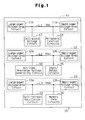
- FIG. 1 is a schematic block circuit diagram of a semiconductor memory device according to one embodiment of the present invention.
- FIG. 2 is a schematic circuit diagram of an internal supply voltage generating circuit of the semiconductor memory device of FIG. 1;
- FIG. 3 is a schematic circuit diagram of a self-refresh oscillation circuit of the semiconductor memory device of FIG. 1;
- FIG. 4 is a graph showing the relationship between an external supply voltage and internal supply voltages that are generated by the internal supply voltage generating circuits.
- a particular example of a semiconductor memory device a synchronous DRAM (SDRAM) 10 , contains internal supply voltage generating circuits according to the preferred embodiment.
- SDRAM synchronous DRAM
- the SDRAM 10 is formed on a 1-chip semiconductor substrate and has a plurality (three in FIG. 1) of internal supply voltage generating circuits 11 , 12 and 13 .
- the first internal supply voltage generating circuit 11 generates a dropped supply voltage Vdd for peripheral circuits supplied to peripheral function circuits 14 .
- the second internal supply voltage generating circuit 12 generates a dropped supply voltage Vddi for input/output circuits supplied to input/output circuits 15 .
- the third internal supply voltage generating circuit 13 generates a dropped supply voltage Vddc for the memory core supplied to memory core circuits 16 .
- the input/output circuits 15 include a plurality of input circuits and output circuits, which constitute the input/output interface of the SDRAM 10 .
- the individual input circuits and output circuits are activated or enabled in active mode and are inactivated or disabled in standby mode or power-down mode.
- the memory core circuits 16 include a sense amplifier and row and column decoders of the SDRAM 10 .
- the individual memory core circuits 16 are enabled in active mode and are disabled in standby mode or power-down mode.
- the peripheral function circuits 14 include a plurality of peripheral circuits excluding the input/output circuits 15 and the memory core circuits 16 .
- the individual peripheral function circuits 14 are enabled in active mode and are disabled in standby mode or power-down mode.
- the internal supply voltage generating circuits 11 , 12 , and 13 have voltage-drop circuits 11 a , 12 a , and 13 a , respectively, for large power (hereinafter referred to as “large-power voltage-drop circuits”) and voltage-drop circuits 11 b , 12 b , and 13 b , respectively, for small power (hereinafter referred to as “small-power voltage-drop circuits”).
- large-power voltage-drop circuits a , 12 a , and 13 a consumes a relatively large current and supplies relatively large drive power.
- Each of the small-power voltage-drop circuits 11 b , 12 b , and 13 b consumes a relatively small current and supplies relatively small drive power.
- the large-power voltage-drop circuit 11 a of the first internal supply voltage generating circuit 11 drops an external supply voltage Vext to generate the stable dropped supply voltage Vdd for peripheral circuits and supplies the dropped supply voltage Vdd to an internal power line L 1 .
- the small-power voltage-drop circuit 11 b of the first internal supply voltage generating circuit 11 drops the external supply voltage Vext to generate the stable dropped supply voltage Vdd for peripheral circuits and supplies the dropped supply voltage Vdd to the internal power line L 1 .
- the large-power voltage-drop circuit 12 a of the second internal supply voltage generating circuit 12 drops the external supply voltage Vext to generate the stable dropped supply voltage Vddi for input/output circuits and supplies the dropped supply voltage Vddi to an internal power line L 2 .
- the small-power voltage-drop circuit 12 b of the second internal supply voltage generating circuit 12 drops the external supply voltage Vext to generate the stable dropped supply voltage Vddi for input/output circuits and supplies the dropped supply voltage Vddi to the internal power line L 2 .
- the large-power voltage-drop circuit 13 a of the third internal supply voltage generating circuit 13 drops the external supply voltage Vext to generate the stable dropped supply voltage Vddc for the memory core and supplies the dropped supply voltage Vddc to an internal power line L 3 .
- the small-power voltage-drop circuit 13 b of the third internal supply voltage generating circuit 13 drops the external supply voltage Vext to generate the stable dropped supply voltage Vddc for the memory core and supplies the dropped supply voltage Vddc to the internal power line L 3 .
- the large-power voltage-drop circuits 11 a , 12 a and 13 a and the small-power voltage-drop circuits 11 b , 12 b and 13 b are enabled.
- the small-power voltage-drop circuits 11 b , 12 b and 13 b may be disabled in active mode.
- the large-power voltage-drop circuits 11 a , 12 a and 13 a are disabled and the small-power voltage-drop circuits 11 b , 12 b and 13 b are enabled.
- the peripheral function circuits 14 are enabled and receive the dropped supply voltage Vdd via the power line L 1 from the large-power voltage-drop circuit 11 a and the small-power voltage-drop circuit 11 b .
- the peripheral function circuits 14 which are disabled in such a mode, are supplied with the dropped supply voltage Vdd via the power line L 1 from the small-power voltage-drop circuit 11 b.
- the input/output circuits 15 are enabled and receive the dropped supply voltage Vddi via the power line L 2 from the large-power voltage-drop circuit 12 a and the small-power voltage-drop circuit 12 b .
- the input/output circuits 15 which are disabled in such a mode, are supplied with the dropped supply voltage Vddi via the power line L 2 from the small-power voltage-drop circuit 12 b.
- the memory core circuits 16 are enabled and receive the dropped supply voltage Vddc via the power line L 3 from the large-power voltage-drop circuit 13 a and the small-power voltage-drop circuit 13 b .
- the memory core circuits 16 which are disabled in such a mode, are supplied with the dropped supply voltage Vddc via the power line L 3 from the small-power voltage-drop circuit 13 b.
- circuits 14 , 15 , and 16 are inactivated in standby mode or power-down mode and activated in the active mode, they are referred to as to-be-controlled internal circuits (first internal circuits).
- a cell-plate voltage generating circuit 17 for memory cells is also connected to the internal power line L 1 .
- the cell-plate voltage generating circuit 17 is always enabled. In active mode, the cell-plate voltage generating circuit 17 operates on the dropped supply voltage Vdd, which is supplied from the large-power voltage-drop circuit 11 a and the small-power voltage-drop circuit 11 b . In standby mode or power-down mode, the circuit 17 operates on the dropped supply voltage Vdd, which is supplied from the small-power voltage-drop circuit 11 b.
- a bit-line precharge voltage generating circuit 18 is also connected to the internal power line L 2 .
- the bit-line precharge voltage generating circuit 18 is always enabled. In active mode, the bit-line precharge voltage generating circuit 18 operates on the dropped supply voltage Vddi, which is supplied from the large-power voltage-drop circuit 12 a and the small-power voltage-drop circuit 12 b . In standby mode or power-down mode, the circuit 18 operates on the dropped supply voltage Vddi, which is supplied from the small-power voltage-drop circuit 12 b.
- a self-refresh oscillation circuit 19 is also connected to the internal power line L 3 .
- the self-refresh oscillation circuit 19 is always enabled. In active mode, the self-refresh oscillation circuit 19 operates on the dropped supply voltage Vddc, which is supplied from the large-power voltage-drop circuit 13 a and the small-power voltage-drop circuit 13 b . In standby mode or power-down mode, the circuit 19 operates on the dropped supply voltage Vddc, which is supplied from the small-power voltage-drop circuit 13 b.
- circuits 17 , 18 , and 19 operate in standby mode or power-down mode and the active mode, they are referred to as constantly-driven internal circuits (second internal circuits).
- Circuits that normally generate DC current may be used in place of the cell-plate voltage generating circuit 17 , the bit-line precharge voltage generating circuit 18 , and the self-refresh oscillation circuit 19 that are respectively connected to the internal supply voltage generating circuits 11 , 12 , and 13 .
- a load circuit, which constantly consumes current, may be connected to any voltage-drop circuit.
- the third internal supply voltage generating circuit 13 is specifically discussed below. Because the first and second internal supply voltage generating circuits 11 and 12 have essentially the same structure as that of the third internal supply voltage generating circuit 13 , their detailed descriptions are not repeated.
- the large-power voltage-drop circuit 13 a which is preferably a differential amplifier, includes a differential amplification circuit that includes first and second N channel MOS (NMOS) transistors TN 1 and TN 2 .
- the sources of the NMOS transistors TN 1 and TN 2 are grounded via a current control NMOS transistor TN 3 .
- An activation control signal ⁇ 1 is supplied to the gate of the current control NMOS transistor TN 3 so that the large-power voltage-drop circuit 13 a is selectively enabled by the activation control signal
- the activation control signal ⁇ 1 is generated by an activation signal generating circuit (not shown).
- the activation signal generating circuit sets the activation control signal ⁇ 1 to a low level when the SDRAM 10 is in standby mode or power-down mode.
- the activation signal generating circuit sets the activation control signal ⁇ 1 to a high level when the SDRAM 10 is changed to active mode from standby mode or power-down mode in response to an active command ACTV.
- the drains of the NMOS transistors TN 1 and TN 2 are connected to the external supply voltage Vext via P channel MOS (PMOS) transistors TP 1 and TP 2 .
- the gates of the PMOS transistors TP 1 and TP 2 are connected together to the drain of the second NMOS transistor TN 2 .
- the gate (inverting input terminal) of the first NMOS transistor TN 1 is supplied with a reference voltage Vref from a reference voltage generating circuit (not shown).
- the gate (non-inverting input terminal) of the second NMOS transistor TN 2 is connected to the internal power line L 3 .
- the drain of the first NMOS transistor TN 1 is connected to the gate of a driving PMOS transistor TP 3 such that the drain voltage of the first NMOS transistor TN 1 is applied to the gate of the PMOS transistor TP 3 .
- the drain of the PMOS transistor TP 3 is connected to the internal power line L 3 , and its source is connected to the external supply voltage Vext.
- a PMOS transistor TP 4 is connected between the gate of the driving PMOS transistor TP 3 and the external supply voltage Vext.
- the gate of the PMOS transistor TP 4 is supplied with the activation control signal ⁇ 1 .
- the PMOS transistor TP 3 is turned off by the low-level activation control signal ⁇ 1 , thereby disabling the large-power voltage-drop circuit 13 a to block the supply of the dropped supply voltage Vddc to the internal power line L 3 .
- the large-power voltage-drop circuit 13 a is enabled and operates such that the voltage (i.e., the dropped supply voltage Vddc on the internal power line L 3 ), which is supplied to the gate of the second NMOS transistor TN 2 , is substantially equal to the reference voltage Vref. That is, the dropped supply voltage Vddc is determined by the reference voltage Vref.
- the large-power voltage-drop circuit 13 a generates a dropped supply voltage Vddc that is constant with respect to the external supply voltage Vext and dependent on the reference voltage Vref. In other words, the large-power voltage-drop circuit 13 a generates a dropped supply voltage Vddc of 2.0 V for the external supply voltage Vext, as shown in FIG. 4 . Even when the external supply voltage Vext is less than a data retention voltage (e.g., 2.3 V), as well as when it lies within the normal operational voltage range of 3.0 V to 3.6 V, the large-power voltage-drop circuit 13 a generates a dropped supply voltage Vddc of 2.0 V.
- the data retention voltage is a voltage in battery data retention mode, in which power consumption becomes low.
- the large-power voltage-drop circuit 11 a of the first internal supply voltage generating circuit 11 generates a dropped supply voltage Vdd of 2.6 V for the external supply voltage Vext.
- the large-power voltage-drop circuit 12 a of the second internal supply voltage generating circuit 12 generates the dropped supply voltage Vddi of 2.3 V with respect to the external supply voltage Vext.
- the dropped supply voltage Vdd and the dropped supply voltage Vddi of the large-power voltage-drop circuits 11 a and 12 a vary with the external supply voltage Vext. This is because the large-power voltage-drop circuit 13 a generates the dropped supply voltage Vddc, which is lower than the dropped supply voltage Vdd and the dropped supply voltage Vddi.
- the small-power voltage-drop circuit 13 b (FIG. 2 ), which is preferably a differential amplifier, includes a differential amplification circuit that has first and second NMOS transistors TN 4 and TN 5 .
- the sources of the NMOS transistors TN 4 and TN 5 are grounded via a current control NMOS transistor TN 6 .
- the gate of the current control NMOS transistor TN 6 is connected to the gate of the first NMOS transistor TN 4 .
- the drains of the NMOS transistors TN 4 and TN 5 are connected to the external supply voltage Vext via PMOS transistors TP 5 and TP 6 .
- the gates of the PMOS transistors TP 5 and TP 6 are connected together to the drain of the second NMOS transistor TN 5 .
- the gate (inverting input terminal) of the first NMOS transistor TN 4 is supplied with the reference voltage Vref. Therefore, the small-power voltage-drop circuit 13 b is always enabled.
- the gate (non-inverting input terminal) of the second NMOS transistor TN 5 is connected to the internal power line L 3 .
- the drain of the first NMOS transistor TN 4 is connected to the gate of a driving PMOS transistor TP 7 such that the drain voltage of the first NMOS transistor TN 4 is applied to the gate of the PMOS transistor TP 7 .
- the drain of the PMOS transistor TP 7 is connected to the internal power line L 3 , and its source is connected to the external supply voltage Vext.
- the small-power voltage-drop circuit 13 b operates such that the voltage (i.e., the dropped supply voltage Vddc on the internal power line L 3 ), which is supplied to the gate of the second NMOS transistor TN 5 , is substantially equal to the reference voltage Vref.
- the small-power voltage-drop circuit 13 b generates a dropped supply voltage Vddc of 2.0 V for the external supply voltage Vext, as shown in FIG. 4 . That is, the small-power voltage-drop circuit 13 b generates the dropped supply voltage Vddc even when the external supply voltage Vext is less than the data retention voltage (e.g., 2.3 V), as well as when it lies within the normal operational voltage range of 3.0 V to 3.6 V.
- the data retention voltage e.g., 2.3 V
- the small-power voltage-drop circuit 11 b generates a dropped supply voltage Vdd of 2.6 V for the external supply voltage Vext, as shown in FIG. 4 .
- the small-power voltage-drop circuit 12 b generates a dropped supply voltage Vddc of 2.3 V for the external supply voltage Vext.
- the dropped supply voltage Vdd and the dropped supply voltage Vddi vary with the external supply voltage Vext.
- the large-power voltage-drop circuit 13 a and the small-power voltage-drop circuit 13 b generate the same dropped supply voltage Vddc, they differ from each other in drive power. That is, the size of the PMOS transistor TP 3 of the large-power voltage-drop circuit 13 a is larger than the size of the PMOS transistor TP 7 of the small-power voltage-drop circuit 13 b.
- the self-refresh oscillation circuit 19 which is connected to the internal power line L 3 , includes an oscillation section with an odd number (five in this example) of inverter circuits 21 to 25 and an output section with a single inverter circuit 26 .
- Each of the inverter circuits 21 - 25 includes a CMOS transistor and receives the dropped supply voltage Vddc via the internal power line L 3 .
- the five inverter circuits 21 - 25 are connected in series such that the output terminal of the last inverter circuit 25 is connected to the input terminal of the first inverter circuit 21 .
- the closed loop connection of the five inverter circuits 21 - 25 generates an oscillation signal that is supplied to the inverter circuit 26 .
- the inverter circuit 26 which includes a CMOS transistor, receives the dropped supply voltage Vddc via the internal power line L 3 .
- the inverter circuit 26 inverts the oscillation signal to generate a refresh clock signal.
- the SDRAM 10 of the preferred embodiment has the following advantages:
- the peripheral function circuits 14 and the cell-plate voltage generating circuit 17 are connected to the first internal supply voltage generating circuit 11 .
- the drive power that is supplied from the small-power voltage-drop circuit 11 b is consumed by the cell-plate voltage generating circuit 17 .
- the drive power of the small-power voltage-drop circuit 11 b is consumed, thereby suppressing a rise in dropped supply voltage Vdd for the peripheral circuits.
- the input/output circuits 15 and the bit-line precharge voltage generating circuit 18 are connected to the second internal supply voltage generating circuit 12 .
- the drive power that is supplied from the small-power voltage-drop circuit 12 b is consumed by the bit-line precharge voltage generating circuit 18 .
- the drive power of the small-power voltage-drop circuit 12 b is consumed, thereby suppressing a rise in dropped supply voltage Vddi for the input/output circuits.
- the memory core circuits 16 and the self-refresh oscillation circuit 19 are connected to the third internal supply voltage generating circuit 13 .
- the drive power that is supplied from the small-power voltage-drop circuit 13 b is consumed by the self-refresh oscillation circuit 19 .
- the drive power of the small-power voltage-drop circuit 13 b is consumed, thereby suppressing a rise in dropped supply voltage Vddc for the memory core.
- the third internal supply voltage generating circuit 13 stably generates the dropped supply voltage Vddc even when the external supply voltage Vext becomes equal to or lower than the data retention voltage. Therefore, the self-refresh oscillation circuit 19 receives the stable dropped supply voltage Vddc of 2.0 V and performs a stable oscillating operation.
- the internal supply voltage generating circuits 11 , 12 and 13 are electrically independent and respectively generate the dropped supply voltages Vdd, Vddi and Vddc, which are different from one another. It is therefore possible to separately design the layout patterns of the internal supply voltage generating circuits 11 , 12 and 13 .
- Each of the peripheral function circuits 14 , the input/output circuits 15 , and the memory core circuits 16 may be separated into smaller circuits so that an internal supply voltage generating circuit is connected to each smaller circuit.
- the present invention may be adapted to a semiconductor memory device or a semiconductor device that has two or four or more internal supply voltage generating circuits that generate different voltages.
- the internal circuits which are constantly driven, are not limited to the cell-plate voltage generating circuit 17 , the bit-line precharge voltage generating circuit 18 and the self-refresh oscillation circuit 19 , but may be other circuits which operate in standby mode or power-down mode, such as a power-on reset circuit that monitors the power supply.
- the cell-plate voltage generating circuit 17 and the bit-line precharge voltage generating circuit 18 may be connected to a single internal supply voltage generating circuit.
- the large-power voltage-drop circuits 11 a , 12 a and 13 a and the small-power voltage-drop circuits 11 b , 12 b and 13 b are preferably feedback type voltage-drop circuits, they may also be source-follower type voltage-drop circuits. That is, it is preferable to use voltage-drop circuits that generate stable dropped supply voltages with respect to the external supply voltage.
- the present invention may be adapted not only to a SDRAM but also to other semiconductor memory devices.
- the present invention may be adapted to a semiconductor device such as an MPU (Microprocessor unit) or a memory controller, as well as a semiconductor memory device.
- a semiconductor device such as an MPU (Microprocessor unit) or a memory controller, as well as a semiconductor memory device.
Landscapes
- Engineering & Computer Science (AREA)
- Microelectronics & Electronic Packaging (AREA)
- Physics & Mathematics (AREA)
- Nonlinear Science (AREA)
- Electromagnetism (AREA)
- General Physics & Mathematics (AREA)
- Radar, Positioning & Navigation (AREA)
- Automation & Control Theory (AREA)
- Dram (AREA)
- Power Sources (AREA)
Abstract
Description
Claims (13)
Applications Claiming Priority (2)
| Application Number | Priority Date | Filing Date | Title |
|---|---|---|---|
| JP2000-022151 | 2000-01-31 | ||
| JP2000022151A JP2001216780A (en) | 2000-01-31 | 2000-01-31 | Driving power supply method for semiconductor device, semiconductor device, driving power supply method for semiconductor storage device, and semiconductor storage device |
Publications (2)
| Publication Number | Publication Date |
|---|---|
| US20010010459A1 US20010010459A1 (en) | 2001-08-02 |
| US6504353B2 true US6504353B2 (en) | 2003-01-07 |
Family
ID=18548485
Family Applications (1)
| Application Number | Title | Priority Date | Filing Date |
|---|---|---|---|
| US09/772,075 Expired - Lifetime US6504353B2 (en) | 2000-01-31 | 2001-01-30 | Drive power supplying method for semiconductor memory device and semiconductor memory device |
Country Status (2)
| Country | Link |
|---|---|
| US (1) | US6504353B2 (en) |
| JP (1) | JP2001216780A (en) |
Cited By (6)
| Publication number | Priority date | Publication date | Assignee | Title |
|---|---|---|---|---|
| US20050024127A1 (en) * | 2003-07-31 | 2005-02-03 | Renesas Technology Corp. | Semiconductor device including reference voltage generation circuit attaining reduced current consumption during stand-by |
| US20050030818A1 (en) * | 2002-08-23 | 2005-02-10 | Micron Technology, Inc. | DRAM power bus control |
| US20070080374A1 (en) * | 2005-10-12 | 2007-04-12 | Semiconductor Energy Laboratory Co., Ltd. | Semiconductor device |
| US20090224823A1 (en) * | 2004-05-25 | 2009-09-10 | Renesas Technology Corp. | Internal voltage generating circuit and semiconductor integrated circuit device |
| US9076510B2 (en) | 2012-02-02 | 2015-07-07 | Samsung Electronics Co., Ltd. | Power mixing circuit and semiconductor memory device including the same |
| US10812138B2 (en) | 2018-08-20 | 2020-10-20 | Rambus Inc. | Pseudo-differential signaling for modified single-ended interface |
Families Citing this family (11)
| Publication number | Priority date | Publication date | Assignee | Title |
|---|---|---|---|---|
| JP4804609B2 (en) * | 2000-02-16 | 2011-11-02 | 富士通セミコンダクター株式会社 | Memory circuit that prevents cell array power supply from rising |
| JP2003022672A (en) * | 2001-07-10 | 2003-01-24 | Sharp Corp | Semiconductor storage device, portable electronic device and detachable storage device |
| US7426151B2 (en) * | 2001-08-14 | 2008-09-16 | Samung Electronics Co., Ltd. | Device and method for performing a partial array refresh operation |
| KR100396897B1 (en) * | 2001-08-14 | 2003-09-02 | 삼성전자주식회사 | Voltage generating circuit for periphery, Semiconductor memory device having the circuit and method thereof |
| KR100605589B1 (en) | 2003-12-30 | 2006-07-28 | 주식회사 하이닉스반도체 | Internal voltage generation circuit of semiconductor device |
| KR100702124B1 (en) * | 2005-04-01 | 2007-03-30 | 주식회사 하이닉스반도체 | Internal voltage supply circuit |
| KR100776738B1 (en) | 2006-04-06 | 2007-11-19 | 주식회사 하이닉스반도체 | Semiconductor memory device |
| JP2009181638A (en) * | 2008-01-30 | 2009-08-13 | Elpida Memory Inc | Semiconductor storage device |
| CN101582293B (en) * | 2008-05-12 | 2012-05-30 | 台湾积体电路制造股份有限公司 | Memory element and method for controlling its word line signal in power cut-off or start-up procedure |
| US8675420B2 (en) * | 2011-05-26 | 2014-03-18 | Micron Technology, Inc. | Devices and systems including enabling circuits |
| US10438646B1 (en) | 2018-07-03 | 2019-10-08 | Micron Technology, Inc. | Apparatuses and methods for providing power for memory refresh operations |
Citations (4)
| Publication number | Priority date | Publication date | Assignee | Title |
|---|---|---|---|---|
| US5461338A (en) * | 1992-04-17 | 1995-10-24 | Nec Corporation | Semiconductor integrated circuit incorporated with substrate bias control circuit |
| US6021082A (en) * | 1997-12-05 | 2000-02-01 | Kabushiki Kaisha Toshiba | Semiconductor memory device including an internal power supply circuit having standby and activation mode |
| US6351179B1 (en) * | 1998-08-17 | 2002-02-26 | Kabushiki Kaisha Toshiba | Semiconductor integrated circuit having active mode and standby mode converters |
| US6385119B2 (en) * | 2000-01-31 | 2002-05-07 | Fujitsu Limited | Internal supply voltage generating cicuit in a semiconductor memory device and method for controlling the same |
-
2000
- 2000-01-31 JP JP2000022151A patent/JP2001216780A/en active Pending
-
2001
- 2001-01-30 US US09/772,075 patent/US6504353B2/en not_active Expired - Lifetime
Patent Citations (4)
| Publication number | Priority date | Publication date | Assignee | Title |
|---|---|---|---|---|
| US5461338A (en) * | 1992-04-17 | 1995-10-24 | Nec Corporation | Semiconductor integrated circuit incorporated with substrate bias control circuit |
| US6021082A (en) * | 1997-12-05 | 2000-02-01 | Kabushiki Kaisha Toshiba | Semiconductor memory device including an internal power supply circuit having standby and activation mode |
| US6351179B1 (en) * | 1998-08-17 | 2002-02-26 | Kabushiki Kaisha Toshiba | Semiconductor integrated circuit having active mode and standby mode converters |
| US6385119B2 (en) * | 2000-01-31 | 2002-05-07 | Fujitsu Limited | Internal supply voltage generating cicuit in a semiconductor memory device and method for controlling the same |
Cited By (16)
| Publication number | Priority date | Publication date | Assignee | Title |
|---|---|---|---|---|
| US20050030818A1 (en) * | 2002-08-23 | 2005-02-10 | Micron Technology, Inc. | DRAM power bus control |
| US7023756B2 (en) * | 2002-08-23 | 2006-04-04 | Micron Technology, Inc. | DRAM power bus control |
| US20060133179A1 (en) * | 2002-08-23 | 2006-06-22 | Micron Technology, Inc. | DRAM power bus control |
| US20070223301A1 (en) * | 2002-08-23 | 2007-09-27 | Micron Technology, Inc. | DRAM power bus control |
| US7277352B2 (en) | 2002-08-23 | 2007-10-02 | Micron Technology, Inc. | DRAM power bus control |
| US20080031071A1 (en) * | 2002-08-23 | 2008-02-07 | Micron Technology, Inc. | DRAM power bus control |
| US7391666B2 (en) | 2002-08-23 | 2008-06-24 | Micron Technology, Inc. | DRAM power bus control |
| US7522466B2 (en) | 2002-08-23 | 2009-04-21 | Micron Technology, Inc. | DRAM power bus control |
| US20050024127A1 (en) * | 2003-07-31 | 2005-02-03 | Renesas Technology Corp. | Semiconductor device including reference voltage generation circuit attaining reduced current consumption during stand-by |
| US20090140798A1 (en) * | 2003-07-31 | 2009-06-04 | Renesas Technology Corp. | Semiconductor device including reference voltage generation circuit attaining reduced current consumption during stand-by |
| US20090224823A1 (en) * | 2004-05-25 | 2009-09-10 | Renesas Technology Corp. | Internal voltage generating circuit and semiconductor integrated circuit device |
| US20070080374A1 (en) * | 2005-10-12 | 2007-04-12 | Semiconductor Energy Laboratory Co., Ltd. | Semiconductor device |
| US7973410B2 (en) * | 2005-10-12 | 2011-07-05 | Semiconductor Energy Laboratory Co., Ltd. | Semiconductor device |
| US9076510B2 (en) | 2012-02-02 | 2015-07-07 | Samsung Electronics Co., Ltd. | Power mixing circuit and semiconductor memory device including the same |
| US10812138B2 (en) | 2018-08-20 | 2020-10-20 | Rambus Inc. | Pseudo-differential signaling for modified single-ended interface |
| US11533077B2 (en) | 2018-08-20 | 2022-12-20 | Rambus Inc. | Pseudo-differential signaling for modified single-ended interface |
Also Published As
| Publication number | Publication date |
|---|---|
| JP2001216780A (en) | 2001-08-10 |
| US20010010459A1 (en) | 2001-08-02 |
Similar Documents
| Publication | Publication Date | Title |
|---|---|---|
| US6504353B2 (en) | Drive power supplying method for semiconductor memory device and semiconductor memory device | |
| JP3704188B2 (en) | Semiconductor memory device | |
| US8014224B2 (en) | Semiconductor device | |
| US7307469B2 (en) | Step-down power supply | |
| US6313695B1 (en) | Semiconductor circuit device having hierarchical power supply structure | |
| KR100648537B1 (en) | Semiconductor integrated circuit and method for generating internal supply voltage in semiconductor integrated circuit | |
| US5097303A (en) | On-chip voltage regulator and semiconductor memory device using the same | |
| JP3510335B2 (en) | Semiconductor memory device, internal power supply voltage generation circuit, internal high voltage generation circuit, intermediate voltage generation circuit, constant current source, and reference voltage generation circuit | |
| US6771117B2 (en) | Semiconductor device less susceptible to variation in threshold voltage | |
| TWI433149B (en) | Sram leakage reduction circuit | |
| US6385119B2 (en) | Internal supply voltage generating cicuit in a semiconductor memory device and method for controlling the same | |
| US7420857B2 (en) | Semiconductor integrated circuit and leak current reducing method | |
| US20020008502A1 (en) | Voltage downconverter circuit capable of reducing current consumption while keeping response rate | |
| JPH10247386A (en) | Boost potential supply circuit and semiconductor memory device | |
| US7751230B2 (en) | Negative voltage generating device | |
| JPH10312683A (en) | Voltage adjusting circuit of semiconductor memory element | |
| JP2002373942A (en) | Semiconductor integrated circuit | |
| US6259280B1 (en) | Class AB amplifier for use in semiconductor memory devices | |
| KR100623616B1 (en) | Semiconductor memory device | |
| JPH05114291A (en) | Generating circuit of reference voltage | |
| US7420358B2 (en) | Internal voltage generating apparatus adaptive to temperature change | |
| JP3410914B2 (en) | Semiconductor integrated circuit | |
| US8228752B2 (en) | Memory circuit and method for controlling memory circuit | |
| JPH0442493A (en) | Semiconductor memory | |
| JPH09320266A (en) | Dynamic random access memory |
Legal Events
| Date | Code | Title | Description |
|---|---|---|---|
| AS | Assignment |
Owner name: FUJITSU LIMITED, JAPAN Free format text: ASSIGNMENT OF ASSIGNORS INTEREST;ASSIGNORS:KOBAYASHI, ISAMU;KATO, YOSHIHARU;REEL/FRAME:011490/0159 Effective date: 20010124 |
|
| STCF | Information on status: patent grant |
Free format text: PATENTED CASE |
|
| FEPP | Fee payment procedure |
Free format text: PAYOR NUMBER ASSIGNED (ORIGINAL EVENT CODE: ASPN); ENTITY STATUS OF PATENT OWNER: LARGE ENTITY |
|
| FPAY | Fee payment |
Year of fee payment: 4 |
|
| AS | Assignment |
Owner name: FUJITSU MICROELECTRONICS LIMITED, JAPAN Free format text: ASSIGNMENT OF ASSIGNORS INTEREST;ASSIGNOR:FUJITSU LIMITED;REEL/FRAME:021998/0645 Effective date: 20081104 Owner name: FUJITSU MICROELECTRONICS LIMITED,JAPAN Free format text: ASSIGNMENT OF ASSIGNORS INTEREST;ASSIGNOR:FUJITSU LIMITED;REEL/FRAME:021998/0645 Effective date: 20081104 |
|
| FPAY | Fee payment |
Year of fee payment: 8 |
|
| AS | Assignment |
Owner name: FUJITSU SEMICONDUCTOR LIMITED, JAPAN Free format text: CHANGE OF NAME;ASSIGNOR:FUJITSU MICROELECTRONICS LIMITED;REEL/FRAME:024982/0245 Effective date: 20100401 |
|
| FPAY | Fee payment |
Year of fee payment: 12 |
|
| AS | Assignment |
Owner name: SOCIONEXT INC., JAPAN Free format text: ASSIGNMENT OF ASSIGNORS INTEREST;ASSIGNOR:FUJITSU SEMICONDUCTOR LIMITED;REEL/FRAME:035508/0637 Effective date: 20150302 |