US6493057B1 - Liquid crystal device and method for manufacturing same with spacers formed by photolithography - Google Patents
Liquid crystal device and method for manufacturing same with spacers formed by photolithography Download PDFInfo
- Publication number
- US6493057B1 US6493057B1 US09/347,834 US34783499A US6493057B1 US 6493057 B1 US6493057 B1 US 6493057B1 US 34783499 A US34783499 A US 34783499A US 6493057 B1 US6493057 B1 US 6493057B1
- Authority
- US
- United States
- Prior art keywords
- substrate
- spacers
- liquid crystal
- substrates
- sealing member
- Prior art date
- Legal status (The legal status is an assumption and is not a legal conclusion. Google has not performed a legal analysis and makes no representation as to the accuracy of the status listed.)
- Expired - Fee Related
Links
Images


Classifications
-
- G—PHYSICS
- G02—OPTICS
- G02F—OPTICAL DEVICES OR ARRANGEMENTS FOR THE CONTROL OF LIGHT BY MODIFICATION OF THE OPTICAL PROPERTIES OF THE MEDIA OF THE ELEMENTS INVOLVED THEREIN; NON-LINEAR OPTICS; FREQUENCY-CHANGING OF LIGHT; OPTICAL LOGIC ELEMENTS; OPTICAL ANALOGUE/DIGITAL CONVERTERS
- G02F1/00—Devices or arrangements for the control of the intensity, colour, phase, polarisation or direction of light arriving from an independent light source, e.g. switching, gating or modulating; Non-linear optics
- G02F1/01—Devices or arrangements for the control of the intensity, colour, phase, polarisation or direction of light arriving from an independent light source, e.g. switching, gating or modulating; Non-linear optics for the control of the intensity, phase, polarisation or colour
- G02F1/13—Devices or arrangements for the control of the intensity, colour, phase, polarisation or direction of light arriving from an independent light source, e.g. switching, gating or modulating; Non-linear optics for the control of the intensity, phase, polarisation or colour based on liquid crystals, e.g. single liquid crystal display cells
- G02F1/133—Constructional arrangements; Operation of liquid crystal cells; Circuit arrangements
- G02F1/1333—Constructional arrangements; Manufacturing methods
- G02F1/1339—Gaskets; Spacers; Sealing of cells
- G02F1/13394—Gaskets; Spacers; Sealing of cells spacers regularly patterned on the cell subtrate, e.g. walls, pillars
-
- G—PHYSICS
- G02—OPTICS
- G02F—OPTICAL DEVICES OR ARRANGEMENTS FOR THE CONTROL OF LIGHT BY MODIFICATION OF THE OPTICAL PROPERTIES OF THE MEDIA OF THE ELEMENTS INVOLVED THEREIN; NON-LINEAR OPTICS; FREQUENCY-CHANGING OF LIGHT; OPTICAL LOGIC ELEMENTS; OPTICAL ANALOGUE/DIGITAL CONVERTERS
- G02F1/00—Devices or arrangements for the control of the intensity, colour, phase, polarisation or direction of light arriving from an independent light source, e.g. switching, gating or modulating; Non-linear optics
- G02F1/01—Devices or arrangements for the control of the intensity, colour, phase, polarisation or direction of light arriving from an independent light source, e.g. switching, gating or modulating; Non-linear optics for the control of the intensity, phase, polarisation or colour
- G02F1/13—Devices or arrangements for the control of the intensity, colour, phase, polarisation or direction of light arriving from an independent light source, e.g. switching, gating or modulating; Non-linear optics for the control of the intensity, phase, polarisation or colour based on liquid crystals, e.g. single liquid crystal display cells
- G02F1/133—Constructional arrangements; Operation of liquid crystal cells; Circuit arrangements
- G02F1/1333—Constructional arrangements; Manufacturing methods
- G02F1/1339—Gaskets; Spacers; Sealing of cells
Definitions
- the present invention relates to a liquid crystal device and a method for manufacturing same.
- FIG. 1 A prior art photoelectric device with liquid crystal is illustrated in FIG. 1 .
- the device such as a liquid crystal display, comprises a pair of substrates 1 and 1 ′ joined to each other with a suitable distance inbetween, a liquid crystal layer 5 disposed between the pair of substrates 1 and 1 ′, opposed electrodes 2 and 2 ′ formed on the opposed inside surfaces of the substrates 1 and 1 ′ in the form of a matrix, and oriented coating 3 and 3 ′ on the opposed insides contiguous to the liquid crystal layer 5 .
- the device can be controlled by applying a voltage selectively to each pixel of the matrix to display an image or picture or storing information in terms of encoded signals.
- the distance between the opposed substrates 1 and 1 ′ is about 10 microns, while devices with the distance of 5 microns are now being developed. Although devices having twisted nematic liquid crystal can be constructed with the distances of this scale, the distance is demanded to be decreased to less than 3 microns, generally 2 ⁇ 0.5 microns, when making use of a ferroelectric liquid crystal for the device in place of a nematic liquid crystal.
- the distance has been kept by disposing spacers 7 and 4 between the pair of substrates 1 and 1 ′.
- two kinds of spacers are illustrated; one being mixed with a sealing member 6 and the other being disposed between the opposed electrodes 2 and 2 ′.
- the spacers 4 are a plurality of spherical particles made of an organic resin such as Micro Pearl SP-210 having the average diameter of 10.0 ⁇ 0.5 microns made of a bridged polymer of divinyl benzene.
- the spacers of Micro Pearl SP-210 are perfect spheres.
- the spacers 4 prevent the substrates 1 and 1 ′ from contact due to unevenness of the substrates or due to external stress.
- the spacers 4 and the electrodes 2 and 2 ′ are in point contact so that the electrodes 2 and 2 ′ are subjected to concentrated stress.
- the concentrated stress may destroy the active devices or disconnect electrode circuits, and therefore make the liquid device defective.
- it is very difficult to obtain a constant distance between the substrates because the spacers, when distributed between the substrates, tend to aggregate to local positions on the substrates and because the diameters of spacers are not constant. Even if uniform distribution of the spacers is obtained between the substrates, the distribution is disturbed during filling process of liquid crystal.
- the liquid crystal is charged into the distance by virtue of capillary action from an opening provided on a portion of sealed-off perimeter of the substrates in the manner that the entrance is dipped in an amount of liquid crystal in a vacuum condition and then the pressure is increased so that the liquid crystal is caused to enter the device through the opening by the differential pressure. So, the stream of the liquid crystal tends to move the distributed spacers. Because of this unevenness of the distance, color shade appears on a display with a ferroelectric liquid crystal which utilizes birefringence. The defect can appear only due to external stress, such as pushing with a finger.
- FIG. 1 is a cross section view showing a prior art liquid crystal device.
- FIGS. 2 (A) to 2 (C) are cross section views showing a process for making a liquid crystal device in accordance with the present invention.
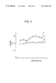
- FIG. 3 is a graphical diagram showing, in relation to the position of the substrate, the distances between pairs of substrates of a liquid crystal device in accordance with the present invention and a prior art liquid crystal device.
- FIGS. 4 (A) and 4 (B) are cross section views showing modifications of devices according to the invention.
- FIGS. 2 (A) to 2 (C) the process for making a liquid crystal device in accordance with the present invention is described.
- the upper surface of a glass substrate 1 is provided with a plurality of first electrode strips 2 made of conductive transparent oxide such as indium tin oxide, SnO 2 or the like and elongated in the direction normal to the drawing.
- the surface is coated with a 500 ⁇ thick oriented thin film 3 made of a polyimide over the first electrode strips.
- the oriented film is treated by rubbing.
- the surface is further coated with an adhesive solution of an epoxy resin, e.g., “UV-307” distributed from Grace Japan Ltd., curable both by ultraviolet light and by thermal energy.
- an epoxy resin e.g., “UV-307” distributed from Grace Japan Ltd., curable both by ultraviolet light and by thermal energy.
- the epoxy resin 8 is applied by a spinner, a roll coater or a spray, or by screen press printing to the thickness of about 20 microns which can be controlled depending on the diameter of spacers.
- the resin is applied to the surface by turning the substrate for 30 minutes at 3000 rpm.
- the epoxy resin layer 8 is exposed to ultraviolet light (10 mW/cm 2 ) through a mask.
- the mask eliminates a portion of the ultraviolet light by photolithography, corresponding to the peripheral portion of the substrate and a plurality of pillars 9 (FIG. 2 (B)).
- the peripheral portion is to be a sealing member 9 ′ and can be formed with an opening for charging a liquid crystal.
- the pillars 9 on the electrode strip 2 have a cross section of 20 microns ⁇ 20 microns respectively with intervals of 400 microns inbetween.
- the uncured portion of the resin layer 8 is removed by a solvent such as acetone, methylethylketone, or the like, and the remaining solvent on the substrate is blown away.
- the substrate provided with the sealing resin layer 9 ′ and the pillars 9 is mated in a vacuum with an opposed substrate 1 ′ which is provided with a plurality of second transparent electrode strips elongated in the direction perpendicular to the first electrode strips 2 as shown in FIG. 2 (C).
- FIG. 2 (C) is illustrated reversed in relation to FIGS. 2 (A) and 2 (B).
- the mated substrates 1 and 1 ′ are fixed by baking at 150° C. for an hour under pressure applied from both external sides of the mated surface. By this postbaking, the thickness is reduced to less than 3 microns, e.g., 2 ⁇ 0.5 microns, which is suitable for a ferroelectric liquid crystal device.
- the distance between the substrates is kept constant even if the substrate is slightly warped because the pillars having a same height urge the substrates to compensate each other.
- a ferroelectric liquid crystal is disposed by an existing method.
- a cross sectional area of the pillars 9 at a middle portion between the first and second substrates is smaller than that at a portion closer to the first substrate.
- the distance between substrates of 200 mm ⁇ 300 mm joined in accordance with the present invention was measured.
- Nine measuring points were taken on the diagonal line of the substrates with an interval of 40 mm.
- 10 designates the results in FIG. 3 .
- 11 designates the corresponding distances of a device produced by a prior art process with spacers made of alumina having 2.0 ⁇ 0.3 microns in diameter which are distributed with methyl alcohol.
- the distance in accordance with the invention is largely constant while the distance in accordance with the prior art is substantially scattered, and particularly is wide at the center position.
- the distance is substantially not changed even when pushed with a finger.
- the fluctuation was only ⁇ 0.5 micron.
- the invention is applied to a liquid crystal panel of 20 cm ⁇ 30 cm formed with an active matrix structure having 400 ⁇ 1920 pixels, the distance between a pair of substrates was also kept constant.
- finely finishing of the surface of a substrate can be dispensed with by means of provision of pillars as explained above.
- the cost of such finishing is higher than the price of a substrate for liquid crystal device, so that the price can be lowered by a factor of 2 to 5.
- sealing process and spacer distributing process are implemented simultaneously.
- spacers are prepared with an interval of 400 microns, corresponding to the interval between adjacent pixels, so that the device constructed with the spacers has resistance against external impact.
- FIGS. 4 (A) and (B) are cross sections showing second and third embodiments of the invention.
- pillars are formed with spheres 12 and adhesive 13 applied to the spheres for maintaining the position of the spheres on the substrates 1 and 1 ′.
- FIG. 4 (B) are prepared to show the pillars 14 can be provided between adjacent electrodes.
- the spacers 9 can be provided in the form of strips or blocks.
Landscapes
- Physics & Mathematics (AREA)
- Nonlinear Science (AREA)
- Mathematical Physics (AREA)
- Chemical & Material Sciences (AREA)
- Crystallography & Structural Chemistry (AREA)
- General Physics & Mathematics (AREA)
- Optics & Photonics (AREA)
- Liquid Crystal (AREA)
Abstract
An improved liquid crystal device and manufacturing method for same are described. In the device, a pair of substrates, between which a liquid crystal layer is disposed, is joined with pillars inbetween functioning as spacers which are provided of photocurable resin by photolithography. With this structure, the spacers can be in surface contact with the inside surfaces of the substrates on which electrode arrangement and active devices are formed.
Description
This application is a Division of application Ser. No. 08/470,618, filed Jun. 6, 1995; which itself is a Division of Ser. No. 08/314,618, filed Sep. 29, 1994, now abandoned which is a division of Ser. No. 07/908,756, filed Jul. 6, 1992, now U.S. Pat. No. 5,379,139; which is a Continuation of Ser. No. 07/440,422, filed Nov. 20, 1989, now abandoned; which is a Continuation-in-Part of Ser. No. 07/087,275, filed Aug. 20, 1987, now abandoned.
The present invention relates to a liquid crystal device and a method for manufacturing same.
A prior art photoelectric device with liquid crystal is illustrated in FIG. 1. The device, such as a liquid crystal display, comprises a pair of substrates 1 and 1′ joined to each other with a suitable distance inbetween, a liquid crystal layer 5 disposed between the pair of substrates 1 and 1′, opposed electrodes 2 and 2′ formed on the opposed inside surfaces of the substrates 1 and 1′ in the form of a matrix, and oriented coating 3 and 3′ on the opposed insides contiguous to the liquid crystal layer 5. By virtue of application of a voltage to the electrodes 2 and 2′, the optical characteristics of the liquid crystal 5 is changed under the electric field induced by the applied voltage. Namely, the device can be controlled by applying a voltage selectively to each pixel of the matrix to display an image or picture or storing information in terms of encoded signals.
The distance between the opposed substrates 1 and 1′ is about 10 microns, while devices with the distance of 5 microns are now being developed. Although devices having twisted nematic liquid crystal can be constructed with the distances of this scale, the distance is demanded to be decreased to less than 3 microns, generally 2±0.5 microns, when making use of a ferroelectric liquid crystal for the device in place of a nematic liquid crystal.
Conventionally, the distance has been kept by disposing spacers 7 and 4 between the pair of substrates 1 and 1′. In the figure, two kinds of spacers are illustrated; one being mixed with a sealing member 6 and the other being disposed between the opposed electrodes 2 and 2′. For example, the spacers 4 are a plurality of spherical particles made of an organic resin such as Micro Pearl SP-210 having the average diameter of 10.0±0.5 microns made of a bridged polymer of divinyl benzene. The spacers of Micro Pearl SP-210 are perfect spheres. The spacers 4 prevent the substrates 1 and 1′ from contact due to unevenness of the substrates or due to external stress.
However, the spacers 4 and the electrodes 2 and 2′ are in point contact so that the electrodes 2 and 2′ are subjected to concentrated stress. In cases where active devices are provided near the electrode 2 and 2′, the concentrated stress may destroy the active devices or disconnect electrode circuits, and therefore make the liquid device defective. Further, even with the spacers 7 and 4, it is very difficult to obtain a constant distance between the substrates because the spacers, when distributed between the substrates, tend to aggregate to local positions on the substrates and because the diameters of spacers are not constant. Even if uniform distribution of the spacers is obtained between the substrates, the distribution is disturbed during filling process of liquid crystal. Especially, when a ferroelectric liquid crystal is disposed between the substrates with 3 microns or less in distance, the liquid crystal is charged into the distance by virtue of capillary action from an opening provided on a portion of sealed-off perimeter of the substrates in the manner that the entrance is dipped in an amount of liquid crystal in a vacuum condition and then the pressure is increased so that the liquid crystal is caused to enter the device through the opening by the differential pressure. So, the stream of the liquid crystal tends to move the distributed spacers. Because of this unevenness of the distance, color shade appears on a display with a ferroelectric liquid crystal which utilizes birefringence. The defect can appear only due to external stress, such as pushing with a finger.
It is therefore an object of the present invention to provide a liquid crystal device with no color shade.
It is another object of the present invention to provide a method for manufacturing a liquid crystal device at high yield.
It is further object of the present invention to provide a liquid crystal device having resistance against external impact.
It is still further object of the present invention to provide a method for manufacturing a liquid crystal device at a low cost.
It is yet still further object of the present invention to provide a facilitated method for manufacturing a liquid crystal device.
FIG. 1 is a cross section view showing a prior art liquid crystal device.
FIGS. 2(A) to 2(C) are cross section views showing a process for making a liquid crystal device in accordance with the present invention.
FIG. 3 is a graphical diagram showing, in relation to the position of the substrate, the distances between pairs of substrates of a liquid crystal device in accordance with the present invention and a prior art liquid crystal device.
FIGS. 4(A) and 4(B) are cross section views showing modifications of devices according to the invention.
Referring now to FIGS. 2(A) to 2(C), the process for making a liquid crystal device in accordance with the present invention is described. In FIG. 2(A), the upper surface of a glass substrate 1 is provided with a plurality of first electrode strips 2 made of conductive transparent oxide such as indium tin oxide, SnO2 or the like and elongated in the direction normal to the drawing. The surface is coated with a 500 Å thick oriented thin film 3 made of a polyimide over the first electrode strips. The oriented film is treated by rubbing. The surface is further coated with an adhesive solution of an epoxy resin, e.g., “UV-307” distributed from Grace Japan Ltd., curable both by ultraviolet light and by thermal energy. The epoxy resin 8 is applied by a spinner, a roll coater or a spray, or by screen press printing to the thickness of about 20 microns which can be controlled depending on the diameter of spacers. For example, the resin is applied to the surface by turning the substrate for 30 minutes at 3000 rpm.
The epoxy resin layer 8 is exposed to ultraviolet light (10 mW/cm2) through a mask. The mask eliminates a portion of the ultraviolet light by photolithography, corresponding to the peripheral portion of the substrate and a plurality of pillars 9 (FIG. 2(B)). The peripheral portion is to be a sealing member 9′ and can be formed with an opening for charging a liquid crystal. The pillars 9 on the electrode strip 2 have a cross section of 20 microns×20 microns respectively with intervals of 400 microns inbetween. The uncured portion of the resin layer 8 is removed by a solvent such as acetone, methylethylketone, or the like, and the remaining solvent on the substrate is blown away. The substrate provided with the sealing resin layer 9′ and the pillars 9 is mated in a vacuum with an opposed substrate 1′ which is provided with a plurality of second transparent electrode strips elongated in the direction perpendicular to the first electrode strips 2 as shown in FIG. 2(C). FIG. 2(C) is illustrated reversed in relation to FIGS. 2(A) and 2(B). The mated substrates 1 and 1′ are fixed by baking at 150° C. for an hour under pressure applied from both external sides of the mated surface. By this postbaking, the thickness is reduced to less than 3 microns, e.g., 2±0.5 microns, which is suitable for a ferroelectric liquid crystal device. In this connection, when at least one substrate is comprised of glass having a thickness of no more than 0.1 mm and has some flexibility, the distance between the substrates is kept constant even if the substrate is slightly warped because the pillars having a same height urge the substrates to compensate each other. Between the mated substrates, a ferroelectric liquid crystal is disposed by an existing method. A cross sectional area of the pillars 9 at a middle portion between the first and second substrates is smaller than that at a portion closer to the first substrate.
As an experiment, the distance between substrates of 200 mm×300 mm joined in accordance with the present invention was measured. Nine measuring points were taken on the diagonal line of the substrates with an interval of 40 mm. 10 designates the results in FIG. 3. For reference, 11 designates the corresponding distances of a device produced by a prior art process with spacers made of alumina having 2.0±0.3 microns in diameter which are distributed with methyl alcohol. As shown in FIG. 3, the distance in accordance with the invention is largely constant while the distance in accordance with the prior art is substantially scattered, and particularly is wide at the center position. In the case of the present invention, the distance is substantially not changed even when pushed with a finger. The fluctuation was only ±0.5 micron. When the invention is applied to a liquid crystal panel of 20 cm×30 cm formed with an active matrix structure having 400×1920 pixels, the distance between a pair of substrates was also kept constant.
Accordingly, finely finishing of the surface of a substrate can be dispensed with by means of provision of pillars as explained above. The cost of such finishing is higher than the price of a substrate for liquid crystal device, so that the price can be lowered by a factor of 2 to 5. Also in accordance with the invention, sealing process and spacer distributing process are implemented simultaneously. Further, spacers are prepared with an interval of 400 microns, corresponding to the interval between adjacent pixels, so that the device constructed with the spacers has resistance against external impact.
FIGS. 4(A) and (B) are cross sections showing second and third embodiments of the invention. In FIG. 4(A), pillars are formed with spheres 12 and adhesive 13 applied to the spheres for maintaining the position of the spheres on the substrates 1 and 1′. FIG. 4(B) are prepared to show the pillars 14 can be provided between adjacent electrodes.
While some embodiments are described supra, the present invention should not limited to these particular embodiments but only limited to the appended claims. Many modifications and variations may cause to those skilled in the art without departing the spirit of the invention. For example, the spacers 9 can be provided in the form of strips or blocks.
Claims (7)
1. An active matrix type liquid crystal display device comprising:
a first substrate;
a plurality of transparent conductive films over said first substrate;
a second substrate opposed to said first substrate with a gap therebetween;
a sealing member provided between said first and second substrates at a perimeter thereof and
a plurality of spacers comprising a resin between said first and second substrates, wherein said spacers are disposed in gaps between adjacent ones of said conductive films and a portion of said transparent conductive films is interposed between said sealing member and said first substrate such that said sealing member partially extends over said transparent conductive film.
2. An active matrix type liquid crystal display device comprising:
a first substrate;
a plurality of pixels arranged in a matrix form over said first substrate;
a second substrate opposed to said first substrate with a gap therebetween;
a sealing member provided between said first and second substrates at a perimeter thereof;
an orientation film formed over said first substrate;
a liquid crystal layer interposed between said first and second substrates;
a plurality of spacers comprising a resin between said first and second substrates,
wherein said spacers are disposed in gaps between adjacent ones of said pixels, and a portion of said orientation film is interposed between said sealing member and said first substrate such that said sealing member partially extends over said transparent conductive film.
3. An active matrix type liquid crystal display device comprising:
a first substrate;
a plurality of transparent conductive films formed over said first substrate;
a second substrate opposed to said first substrate with a gap therebetween;
a plurality of spacers comprising a resin between said first and second substrates wherein a cross sectional area of said spacers at a middle portion between said first and second substrates is smaller than that at a portion closer to said first substrate; and
a sealing member disposed between said first and second substrates at a perimeter thereof,
wherein said spacers are disposed in gaps between adjacent ones of said conductive films,
wherein a portion of said transparent conductive films is interposed between said sealing member and said first substrate such that said sealing member partially extends over said transparent conductive film.
4. An active matrix type liquid crystal display device comprising:
a first substrate;
a plurality of transparent conductive films formed over said first substrate;
an orientation control film formed over said plurality of transparent conductive films;
a second substrate opposed to said first substrate with a gap therebetween;
a sealing member disposed between said first and second substrates at a perimeter thereof and
a plurality of spacers comprising a resin between said first and second substrates wherein said spacers are directly adhered to said orientation control film,
wherein said spacers are disposed in gaps between adjacent ones of said conductive films and a portion of said orientation control film and a portion of said transparent conductive films are disposed between said sealing member and said first substrate such that said sealing member partially extends over said transparent conductive film.
5. The active matrix type liquid crystal display device according to any one of claims 1, 2, 3 and 4 wherein said spacers are in the shape of a block.
6. The active matrix type liquid crystal display device according to any one of claims 1, 2, 3 and 4 wherein said spacers are formed by patterning using a mask.
7. The active matrix type liquid crystal display device according to any one of claims 1, 2, 3 and 4 wherein said spacers consist essentially of resin.
Priority Applications (2)
| Application Number | Priority Date | Filing Date | Title |
|---|---|---|---|
| US09/347,834 US6493057B1 (en) | 1986-08-20 | 1999-07-02 | Liquid crystal device and method for manufacturing same with spacers formed by photolithography |
| US10/304,706 US6853431B2 (en) | 1986-08-20 | 2002-11-27 | Liquid crystal device and method for manufacturing same with spacers formed by photolithography |
Applications Claiming Priority (8)
| Application Number | Priority Date | Filing Date | Title |
|---|---|---|---|
| JP61196424A JPS6350817A (en) | 1986-08-20 | 1986-08-20 | Method for forming liquid crystal electrooptical device |
| JP61-196424 | 1986-08-20 | ||
| US8727587A | 1987-08-20 | 1987-08-20 | |
| US44042289A | 1989-11-20 | 1989-11-20 | |
| US07/908,756 US5379139A (en) | 1986-08-20 | 1992-07-06 | Liquid crystal device and method for manufacturing same with spacers formed by photolithography |
| US31461894A | 1994-09-29 | 1994-09-29 | |
| US08/470,618 US5963288A (en) | 1987-08-20 | 1995-06-06 | Liquid crystal device having sealant and spacers made from the same material |
| US09/347,834 US6493057B1 (en) | 1986-08-20 | 1999-07-02 | Liquid crystal device and method for manufacturing same with spacers formed by photolithography |
Related Parent Applications (1)
| Application Number | Title | Priority Date | Filing Date |
|---|---|---|---|
| US08/470,618 Division US5963288A (en) | 1986-08-20 | 1995-06-06 | Liquid crystal device having sealant and spacers made from the same material |
Related Child Applications (1)
| Application Number | Title | Priority Date | Filing Date |
|---|---|---|---|
| US10/304,706 Division US6853431B2 (en) | 1986-08-20 | 2002-11-27 | Liquid crystal device and method for manufacturing same with spacers formed by photolithography |
Publications (1)
| Publication Number | Publication Date |
|---|---|
| US6493057B1 true US6493057B1 (en) | 2002-12-10 |
Family
ID=27492123
Family Applications (4)
| Application Number | Title | Priority Date | Filing Date |
|---|---|---|---|
| US08/470,618 Expired - Lifetime US5963288A (en) | 1986-08-20 | 1995-06-06 | Liquid crystal device having sealant and spacers made from the same material |
| US08/871,129 Expired - Fee Related US5952676A (en) | 1986-08-20 | 1997-06-06 | Liquid crystal device and method for manufacturing same with spacers formed by photolithography |
| US09/347,834 Expired - Fee Related US6493057B1 (en) | 1986-08-20 | 1999-07-02 | Liquid crystal device and method for manufacturing same with spacers formed by photolithography |
| US10/304,706 Expired - Fee Related US6853431B2 (en) | 1986-08-20 | 2002-11-27 | Liquid crystal device and method for manufacturing same with spacers formed by photolithography |
Family Applications Before (2)
| Application Number | Title | Priority Date | Filing Date |
|---|---|---|---|
| US08/470,618 Expired - Lifetime US5963288A (en) | 1986-08-20 | 1995-06-06 | Liquid crystal device having sealant and spacers made from the same material |
| US08/871,129 Expired - Fee Related US5952676A (en) | 1986-08-20 | 1997-06-06 | Liquid crystal device and method for manufacturing same with spacers formed by photolithography |
Family Applications After (1)
| Application Number | Title | Priority Date | Filing Date |
|---|---|---|---|
| US10/304,706 Expired - Fee Related US6853431B2 (en) | 1986-08-20 | 2002-11-27 | Liquid crystal device and method for manufacturing same with spacers formed by photolithography |
Country Status (1)
| Country | Link |
|---|---|
| US (4) | US5963288A (en) |
Cited By (5)
| Publication number | Priority date | Publication date | Assignee | Title |
|---|---|---|---|---|
| US20020039166A1 (en) * | 2000-10-04 | 2002-04-04 | Song Jang-Kun | Liquid crystal display |
| US20020149734A1 (en) * | 2001-04-13 | 2002-10-17 | Melnik George A. | Liquid crystal display device having uniform integrated spacers |
| CN100405167C (en) * | 2006-04-24 | 2008-07-23 | 友达光电股份有限公司 | Color filter substrate and manufacturing method thereof |
| US20080218679A1 (en) * | 2007-03-05 | 2008-09-11 | Samsung Electronics Co., Ltd. | Display device and manufacturing method thereof |
| US20090244457A1 (en) * | 2005-09-22 | 2009-10-01 | Sharp Kabushiki Kaisha | Liquid crystal display device |
Families Citing this family (165)
| Publication number | Priority date | Publication date | Assignee | Title |
|---|---|---|---|---|
| US5963288A (en) * | 1987-08-20 | 1999-10-05 | Semiconductor Energy Laboratory Co., Ltd. | Liquid crystal device having sealant and spacers made from the same material |
| JP3205373B2 (en) * | 1992-03-12 | 2001-09-04 | 株式会社日立製作所 | Liquid crystal display |
| JP3173854B2 (en) | 1992-03-25 | 2001-06-04 | 株式会社半導体エネルギー研究所 | Method for manufacturing thin-film insulated gate semiconductor device and semiconductor device manufactured |
| US6888608B2 (en) * | 1995-09-06 | 2005-05-03 | Kabushiki Kaisha Toshiba | Liquid crystal display device |
| US6288764B1 (en) * | 1996-06-25 | 2001-09-11 | Semiconductor Energy Laboratory Co., Ltd. | Display device or electronic device having liquid crystal display panel |
| US6266121B1 (en) * | 1996-11-28 | 2001-07-24 | Sharp Kabushiki Kaisha | Liquid crystal display element and method of manufacturing same |
| JP4028043B2 (en) * | 1997-10-03 | 2007-12-26 | コニカミノルタホールディングス株式会社 | Liquid crystal light modulation device and method for manufacturing liquid crystal light modulation device |
| JP3441047B2 (en) * | 1997-10-24 | 2003-08-25 | シャープ株式会社 | Liquid crystal display device and manufacturing method thereof |
| JPH11202349A (en) * | 1998-01-12 | 1999-07-30 | Semiconductor Energy Lab Co Ltd | Display device |
| US6292249B1 (en) * | 1998-06-30 | 2001-09-18 | Philips Electronics North America Corporation | Uniform cell-gap spacing in LCD |
| JP4069991B2 (en) | 1998-08-10 | 2008-04-02 | 株式会社 日立ディスプレイズ | Liquid crystal display |
| JP4168488B2 (en) * | 1998-08-28 | 2008-10-22 | ソニー株式会社 | Liquid crystal display |
| JP4298131B2 (en) | 1999-05-14 | 2009-07-15 | 株式会社半導体エネルギー研究所 | Method for manufacturing liquid crystal display device |
| US6680487B1 (en) * | 1999-05-14 | 2004-01-20 | Semiconductor Energy Laboratory Co., Ltd. | Semiconductor comprising a TFT provided on a substrate having an insulating surface and method of fabricating the same |
| TW459275B (en) * | 1999-07-06 | 2001-10-11 | Semiconductor Energy Lab | Semiconductor device and method of fabricating the same |
| US6580094B1 (en) * | 1999-10-29 | 2003-06-17 | Semiconductor Energy Laboratory Co., Ltd. | Electro luminescence display device |
| JP4445077B2 (en) * | 1999-11-16 | 2010-04-07 | 東芝モバイルディスプレイ株式会社 | Active matrix type liquid crystal display device |
| US7002659B1 (en) | 1999-11-30 | 2006-02-21 | Semiconductor Energy Laboratory Co., Ltd. | Liquid crystal panel and liquid crystal projector |
| US7071041B2 (en) * | 2000-01-20 | 2006-07-04 | Semiconductor Energy Laboratory Co., Ltd. | Method of manufacturing a semiconductor device |
| JP2002006325A (en) * | 2000-06-20 | 2002-01-09 | Nec Corp | Method for manufacturing liquid crystal display panel |
| JP3823016B2 (en) * | 2000-07-21 | 2006-09-20 | 株式会社日立製作所 | Liquid crystal display |
| JP3936126B2 (en) * | 2000-08-30 | 2007-06-27 | シャープ株式会社 | Transflective liquid crystal display device |
| JP2002082358A (en) * | 2000-09-06 | 2002-03-22 | Sony Corp | Light control device and imaging device |
| JP2002333632A (en) * | 2001-05-10 | 2002-11-22 | Nec Corp | Manufacturing method for liquid crystal display device |
| JP2003057660A (en) * | 2001-06-05 | 2003-02-26 | Sharp Corp | Liquid crystal display element and liquid crystal display device using the same |
| TWI285279B (en) * | 2001-06-14 | 2007-08-11 | Himax Tech Ltd | Liquid crystal display panel having sealant |
| US7230670B2 (en) | 2001-10-05 | 2007-06-12 | Lg.Philips Lcd Co., Ltd. | Method for fabricating LCD |
| US6819391B2 (en) | 2001-11-30 | 2004-11-16 | Lg. Philips Lcd Co., Ltd. | Liquid crystal display panel having dummy column spacer with opened portion |
| KR100685948B1 (en) * | 2001-12-14 | 2007-02-23 | 엘지.필립스 엘시디 주식회사 | LCD and its manufacturing method |
| US7292304B2 (en) * | 2001-12-17 | 2007-11-06 | Lg.Philips Lcd Co., Ltd. | Liquid crystal display panel and method for fabricating the same comprising a dummy column spacer to regulate a liquid crystal flow and a supplemental dummy column spacer formed substantially parallel and along the dummy column spacer |
| KR100652045B1 (en) * | 2001-12-21 | 2006-11-30 | 엘지.필립스 엘시디 주식회사 | LCD and its manufacturing method |
| KR100652046B1 (en) * | 2001-12-22 | 2006-11-30 | 엘지.필립스 엘시디 주식회사 | LCD and its manufacturing method |
| KR100685949B1 (en) * | 2001-12-22 | 2007-02-23 | 엘지.필립스 엘시디 주식회사 | LCD and its manufacturing method |
| US7362407B2 (en) * | 2002-02-01 | 2008-04-22 | Lg.Philips Lcd Co., Ltd. | Method of fabricating liquid crystal display device |
| KR100510718B1 (en) * | 2002-02-04 | 2005-08-30 | 엘지.필립스 엘시디 주식회사 | manufacturing device for manufacturing of liquid crystal device |
| KR100510719B1 (en) | 2002-02-05 | 2005-08-30 | 엘지.필립스 엘시디 주식회사 | Method for manufacturing liquid crystal display device |
| JP2003233080A (en) * | 2002-02-05 | 2003-08-22 | Lg Phillips Lcd Co Ltd | Coupling device and method of manufacturing liquid crystal display device using the same |
| KR100469353B1 (en) * | 2002-02-06 | 2005-02-02 | 엘지.필립스 엘시디 주식회사 | bonding device for liquid crystal display |
| KR100817129B1 (en) * | 2002-02-07 | 2008-03-27 | 엘지.필립스 엘시디 주식회사 | Cutting device and method of liquid crystal panel |
| US7410109B2 (en) | 2002-02-07 | 2008-08-12 | Lg Display Co., Ltd. | Liquid crystal dispensing apparatus with nozzle protecting device |
| KR100789454B1 (en) | 2002-02-09 | 2007-12-31 | 엘지.필립스 엘시디 주식회사 | Cutting device and method of liquid crystal panel |
| KR100832292B1 (en) * | 2002-02-19 | 2008-05-26 | 엘지디스플레이 주식회사 | Liquid crystal panel cutting device |
| KR100505180B1 (en) * | 2002-02-20 | 2005-08-01 | 엘지.필립스 엘시디 주식회사 | A liquid crystal dispensing apparatus with a nozzle cleaning device and a method of dispensing liquid crystal using thereof |
| KR100469359B1 (en) * | 2002-02-20 | 2005-02-02 | 엘지.필립스 엘시디 주식회사 | bonding device for liquid crystal display |
| KR100532083B1 (en) * | 2002-02-20 | 2005-11-30 | 엘지.필립스 엘시디 주식회사 | A liquid crystal dispensing apparatus having an integrated needle sheet |
| KR100672641B1 (en) * | 2002-02-20 | 2007-01-23 | 엘지.필립스 엘시디 주식회사 | LCD and its manufacturing method |
| US6824023B2 (en) | 2002-02-20 | 2004-11-30 | Lg. Philips Lcd Co., Ltd. | Liquid crystal dispensing apparatus |
| KR100789455B1 (en) | 2002-02-20 | 2007-12-31 | 엘지.필립스 엘시디 주식회사 | Cutting method of liquid crystal panel |
| US7006202B2 (en) * | 2002-02-21 | 2006-02-28 | Lg.Philips Lcd Co., Ltd. | Mask holder for irradiating UV-rays |
| KR100469508B1 (en) | 2002-02-22 | 2005-02-02 | 엘지.필립스 엘시디 주식회사 | A liquid crystal dispensing apparatus having controlling function of dropping amount caused by controlling tension of spring |
| KR100469360B1 (en) * | 2002-02-22 | 2005-02-02 | 엘지.필립스 엘시디 주식회사 | bonding device for liquid crystal display and operation method thereof |
| US6800172B2 (en) * | 2002-02-22 | 2004-10-05 | Micron Technology, Inc. | Interfacial structure for semiconductor substrate processing chambers and substrate transfer chambers and for semiconductor substrate processing chambers and accessory attachments, and semiconductor substrate processor |
| US6864948B2 (en) * | 2002-02-22 | 2005-03-08 | Lg.Philips Lcd Co., Ltd. | Apparatus for measuring dispensing amount of liquid crystal drops and method for manufacturing liquid crystal display device using the same |
| KR100741897B1 (en) * | 2002-03-22 | 2007-07-24 | 엘지.필립스 엘시디 주식회사 | Bonding device with gas temperature control |
| US6712883B2 (en) * | 2002-02-25 | 2004-03-30 | Lg.Philips Lcd Co., Ltd. | Apparatus and method for deaerating liquid crystal |
| US6803984B2 (en) | 2002-02-25 | 2004-10-12 | Lg.Philips Lcd Co., Ltd. | Method and apparatus for manufacturing liquid crystal display device using serial production processes |
| US8074551B2 (en) * | 2002-02-26 | 2011-12-13 | Lg Display Co., Ltd. | Cutting wheel for liquid crystal display panel |
| KR100720414B1 (en) * | 2002-02-27 | 2007-05-22 | 엘지.필립스 엘시디 주식회사 | Manufacturing Method Of Liquid Crystal Display |
| KR100511352B1 (en) | 2002-02-27 | 2005-08-31 | 엘지.필립스 엘시디 주식회사 | An apparatus for dispensing liquid crystal and a method of controlling liquid crystal dropping amount |
| US6784970B2 (en) * | 2002-02-27 | 2004-08-31 | Lg.Philips Lcd Co., Ltd. | Method of fabricating LCD |
| US7270587B2 (en) * | 2002-03-05 | 2007-09-18 | Lg.Philips Lcd Co., Ltd. | Apparatus and method for manufacturing liquid crystal display devices, method for using the apparatus, and device produced by the method |
| KR100798320B1 (en) * | 2002-03-06 | 2008-01-28 | 엘지.필립스 엘시디 주식회사 | Inspection device and method of liquid crystal panel |
| KR100662495B1 (en) * | 2002-03-07 | 2007-01-02 | 엘지.필립스 엘시디 주식회사 | Manufacturing method of liquid crystal display device |
| US7416010B2 (en) * | 2002-03-08 | 2008-08-26 | Lg Display Co., Ltd. | Bonding apparatus and system for fabricating liquid crystal display device |
| JP2003270652A (en) * | 2002-03-08 | 2003-09-25 | Lg Phillips Lcd Co Ltd | Liquid crystal diffusion control device and liquid crystal display device manufacturing method |
| KR100720415B1 (en) | 2002-03-08 | 2007-05-22 | 엘지.필립스 엘시디 주식회사 | Carrier for liquid crystal display device manufacturing process |
| KR100807587B1 (en) * | 2002-03-09 | 2008-02-28 | 엘지.필립스 엘시디 주식회사 | Cutting method of liquid crystal panel |
| US7027122B2 (en) * | 2002-03-12 | 2006-04-11 | Lg.Philips Lcd Co., Ltd. | Bonding apparatus having compensating system for liquid crystal display device and method for manufacturing the same |
| KR100817130B1 (en) * | 2002-03-13 | 2008-03-27 | 엘지.필립스 엘시디 주식회사 | Polishing detection pattern of liquid crystal panel and polishing failure determination method using the same |
| US6892437B2 (en) * | 2002-03-13 | 2005-05-17 | Lg. Philips Lcd Co., Ltd. | Apparatus and method for manufacturing liquid crystal display device |
| KR100817132B1 (en) * | 2002-03-15 | 2008-03-27 | 엘지.필립스 엘시디 주식회사 | LCD Dropping Device |
| KR100870661B1 (en) * | 2002-03-15 | 2008-11-26 | 엘지디스플레이 주식회사 | Board storage cassette |
| US6782928B2 (en) | 2002-03-15 | 2004-08-31 | Lg.Philips Lcd Co., Ltd. | Liquid crystal dispensing apparatus having confirming function for remaining amount of liquid crystal and method for measuring the same |
| US7698833B2 (en) * | 2002-03-15 | 2010-04-20 | Lg Display Co., Ltd. | Apparatus for hardening a sealant located between a pair bonded substrates of liquid crystal display device |
| US6885427B2 (en) * | 2002-03-15 | 2005-04-26 | Lg.Philips Lcd Co., Ltd. | Substrate bonding apparatus for liquid crystal display device having alignment system with one end provided inside vacuum chamber |
| KR100817131B1 (en) * | 2002-03-15 | 2008-03-27 | 엘지.필립스 엘시디 주식회사 | Inspection device and method of liquid crystal panel |
| KR100720416B1 (en) * | 2002-03-16 | 2007-05-22 | 엘지.필립스 엘시디 주식회사 | Bonding device for liquid crystal display device |
| KR100685952B1 (en) * | 2002-03-19 | 2007-02-23 | 엘지.필립스 엘시디 주식회사 | Substrate for liquid crystal display device, liquid crystal display device and manufacturing method thereof |
| US7341641B2 (en) * | 2002-03-20 | 2008-03-11 | Lg.Philips Lcd Co., Ltd. | Bonding device for manufacturing liquid crystal display device |
| KR100854378B1 (en) * | 2002-03-20 | 2008-08-26 | 엘지디스플레이 주식회사 | Liquid crystal panel and its manufacturing method |
| KR100652050B1 (en) * | 2002-03-20 | 2006-11-30 | 엘지.필립스 엘시디 주식회사 | LCD and its manufacturing method |
| KR100832293B1 (en) * | 2002-03-20 | 2008-05-26 | 엘지디스플레이 주식회사 | Polishing table for liquid crystal panel and polishing device using the same |
| US6827240B2 (en) | 2002-03-21 | 2004-12-07 | Lg.Philips Lcd Co., Ltd. | Liquid crystal dispensing apparatus |
| US6874662B2 (en) * | 2002-03-21 | 2005-04-05 | Lg. Philips Lcd Co., Ltd. | Liquid crystal dispensing apparatus |
| KR100841623B1 (en) * | 2002-03-21 | 2008-06-27 | 엘지디스플레이 주식회사 | Polishing device for liquid crystal panel |
| KR100798322B1 (en) * | 2002-03-21 | 2008-01-28 | 엘지.필립스 엘시디 주식회사 | Polishing amount correction device and method of liquid crystal panel |
| US6793756B2 (en) * | 2002-03-22 | 2004-09-21 | Lg. Phillips Lcd Co., Ltd. | Substrate bonding apparatus for liquid crystal display device and method for driving the same |
| JP4210139B2 (en) * | 2002-03-23 | 2009-01-14 | エルジー ディスプレイ カンパニー リミテッド | Liquid crystal dropping device capable of adjusting the dropping amount of liquid crystal depending on the height of the spacer and dropping method thereof |
| KR100885840B1 (en) * | 2002-03-23 | 2009-02-27 | 엘지디스플레이 주식회사 | Liquid crystal panel structure capable of compensating cell gap |
| US7244160B2 (en) * | 2002-03-23 | 2007-07-17 | Lg.Philips Lcd Co., Ltd. | Liquid crystal display device bonding apparatus and method of using the same |
| KR100860522B1 (en) * | 2002-03-23 | 2008-09-26 | 엘지디스플레이 주식회사 | Liquid Crystal Panel Transfer Device |
| KR100640994B1 (en) * | 2002-03-25 | 2006-11-02 | 엘지.필립스 엘시디 주식회사 | Seal material defoaming container and seal material defoaming equipment using the same |
| KR100817134B1 (en) * | 2002-03-25 | 2008-03-27 | 엘지.필립스 엘시디 주식회사 | Liquid crystal panel manufacturing apparatus and method |
| KR100848556B1 (en) * | 2002-03-25 | 2008-07-25 | 엘지디스플레이 주식회사 | Rotation buffer of liquid crystal panel and rubbing device using the same |
| KR100685923B1 (en) * | 2002-03-25 | 2007-02-23 | 엘지.필립스 엘시디 주식회사 | Bonding device and manufacturing method of liquid crystal display device using the same |
| KR100720420B1 (en) * | 2002-03-25 | 2007-05-22 | 엘지.필립스 엘시디 주식회사 | Operation control method of bonding apparatus for liquid crystal display device and apparatus therefor |
| TW595263B (en) * | 2002-04-12 | 2004-06-21 | O2Micro Inc | A circuit structure for driving cold cathode fluorescent lamp |
| US7225917B2 (en) * | 2002-06-15 | 2007-06-05 | Lg.Philips Lcd Co., Ltd. | Conveyor system having width adjustment unit |
| US7295279B2 (en) | 2002-06-28 | 2007-11-13 | Lg.Philips Lcd Co., Ltd. | System and method for manufacturing liquid crystal display devices |
| JP2004045614A (en) * | 2002-07-10 | 2004-02-12 | Seiko Epson Corp | Liquid crystal device, manufacturing method of liquid crystal device, electronic equipment |
| KR100488535B1 (en) * | 2002-07-20 | 2005-05-11 | 엘지.필립스 엘시디 주식회사 | Apparatus for dispensing Liquid crystal and method for dispensing thereof |
| JP4338948B2 (en) * | 2002-08-01 | 2009-10-07 | 株式会社半導体エネルギー研究所 | Method for producing carbon nanotube semiconductor device |
| KR100675628B1 (en) * | 2002-10-16 | 2007-02-01 | 엘지.필립스 엘시디 주식회사 | Insulation Etching Equipment and Etching Method |
| KR100724474B1 (en) * | 2002-10-22 | 2007-06-04 | 엘지.필립스 엘시디 주식회사 | Device for cutting liquid crystal display panel and method for cutting the same |
| KR100493384B1 (en) * | 2002-11-07 | 2005-06-07 | 엘지.필립스 엘시디 주식회사 | structure for loading of substrate in substrate bonding device for manucturing a liquid crystal display device |
| KR100689310B1 (en) * | 2002-11-11 | 2007-03-08 | 엘지.필립스 엘시디 주식회사 | Dispenser of liquid crystal display panel and gap control method of nozzle and substrate using same |
| KR100618576B1 (en) * | 2002-11-13 | 2006-08-31 | 엘지.필립스 엘시디 주식회사 | Dispenser of liquid crystal display panel and dispensing method using the same |
| KR100618577B1 (en) | 2002-11-13 | 2006-08-31 | 엘지.필립스 엘시디 주식회사 | Dispenser of liquid crystal display panel and dispensing method using the same |
| KR100724475B1 (en) * | 2002-11-13 | 2007-06-04 | 엘지.필립스 엘시디 주식회사 | Seal dispenser of liquid crystal display panel and disconnection detection method of seal pattern using the same |
| KR100724476B1 (en) * | 2002-11-13 | 2007-06-04 | 엘지.필립스 엘시디 주식회사 | Dispenser of liquid crystal display panel and method for detecting residual amount of dispensing material using same |
| KR100720422B1 (en) | 2002-11-15 | 2007-05-22 | 엘지.필립스 엘시디 주식회사 | Liquid crystal display device manufacturing apparatus and manufacturing method using the same |
| US7275577B2 (en) * | 2002-11-16 | 2007-10-02 | Lg.Philips Lcd Co., Ltd. | Substrate bonding machine for liquid crystal display device |
| TWI257515B (en) * | 2002-11-16 | 2006-07-01 | Lg Philips Lcd Co Ltd | Substrate bonding apparatus for liquid crystal display device |
| KR100662497B1 (en) | 2002-11-18 | 2007-01-02 | 엘지.필립스 엘시디 주식회사 | Substrate bonding device for liquid crystal display device manufacturing process |
| KR100724477B1 (en) * | 2002-11-19 | 2007-06-04 | 엘지.필립스 엘시디 주식회사 | Dispenser of liquid crystal display panel and dispensing method using same |
| KR100710163B1 (en) | 2002-11-28 | 2007-04-20 | 엘지.필립스 엘시디 주식회사 | method for manufacturing of LCD |
| KR100710162B1 (en) * | 2002-11-28 | 2007-04-20 | 엘지.필립스 엘시디 주식회사 | Seal pattern forming method of liquid crystal display |
| KR100832297B1 (en) * | 2002-12-17 | 2008-05-26 | 엘지디스플레이 주식회사 | Polishing amount measuring device and measuring method of liquid crystal display panel |
| KR100700176B1 (en) * | 2002-12-18 | 2007-03-27 | 엘지.필립스 엘시디 주식회사 | Dispenser of liquid crystal display panel and gap control method of nozzle and substrate using same |
| KR100771907B1 (en) * | 2002-12-20 | 2007-11-01 | 엘지.필립스 엘시디 주식회사 | Dispenser and Dispensing Method of Liquid Crystal Display Panel |
| KR100618578B1 (en) * | 2002-12-20 | 2006-08-31 | 엘지.필립스 엘시디 주식회사 | Dispenser of liquid crystal display panel and dispensing method using the same |
| KR100618579B1 (en) * | 2002-12-23 | 2006-08-31 | 엘지.필립스 엘시디 주식회사 | Dispenser Aligner and Method |
| KR100652212B1 (en) * | 2002-12-30 | 2006-11-30 | 엘지.필립스 엘시디 주식회사 | Manufacturing method of liquid crystal panel and seal pattern forming apparatus used therein |
| KR100652213B1 (en) * | 2002-12-31 | 2006-11-30 | 엘지.필립스 엘시디 주식회사 | LCD and its manufacturing method |
| KR100996576B1 (en) | 2003-05-09 | 2010-11-24 | 주식회사 탑 엔지니어링 | Liquid crystal dropping device and liquid crystal dropping method |
| KR100923680B1 (en) * | 2003-04-29 | 2009-10-28 | 엘지디스플레이 주식회사 | Liquid Crystal Display Panel Cutting Device |
| KR100939629B1 (en) * | 2003-06-02 | 2010-01-29 | 엘지디스플레이 주식회사 | Syringe of liquid crystal display panel |
| KR20040104037A (en) * | 2003-06-02 | 2004-12-10 | 엘지.필립스 엘시디 주식회사 | Dispenser for liquid crystal display panel |
| KR100557500B1 (en) * | 2003-06-24 | 2006-03-07 | 엘지.필립스 엘시디 주식회사 | Liquid crystal dropping device which can read information of liquid crystal container and liquid crystal dropping method using the same |
| KR100566455B1 (en) * | 2003-06-24 | 2006-03-31 | 엘지.필립스 엘시디 주식회사 | Liquid crystal dropping device and liquid crystal dropping method using spacer information |
| KR100996554B1 (en) * | 2003-06-24 | 2010-11-24 | 엘지디스플레이 주식회사 | Liquid crystal dropping device with detachable liquid crystal discharge pump |
| KR100966451B1 (en) | 2003-06-25 | 2010-06-28 | 엘지디스플레이 주식회사 | LCD Dropping Device |
| KR100495476B1 (en) * | 2003-06-27 | 2005-06-14 | 엘지.필립스 엘시디 주식회사 | Liquid crystal dispensing system |
| US6892769B2 (en) | 2003-06-30 | 2005-05-17 | Lg.Philips Lcd Co., Ltd. | Substrate bonding apparatus for liquid crystal display device panel |
| KR20050005881A (en) * | 2003-07-07 | 2005-01-15 | 삼성전자주식회사 | Liquid crystal display device |
| WO2005012991A1 (en) * | 2003-08-04 | 2005-02-10 | Koninklijke Philips Electronics N.V. | Display device and method for manufacturing a display device |
| US20070019150A1 (en) * | 2003-09-04 | 2007-01-25 | Koninklijke Philips Electronics N.V. | Display device with spacers and seals and the method of manufacture thereof |
| KR20050041697A (en) | 2003-10-31 | 2005-05-04 | 엘지.필립스 엘시디 주식회사 | Apparatus for rubbing liquid crystal display panel |
| CN100362399C (en) | 2003-11-17 | 2008-01-16 | Lg.菲利浦Lcd株式会社 | Liquid crystal dispensing method and apparatus |
| KR100689313B1 (en) * | 2003-11-22 | 2007-03-08 | 엘지.필립스 엘시디 주식회사 | Silver-Silent Hybrid Dispenser and Dispensing Method of Liquid Crystal Display Panel Using Same Dispenser |
| KR100987897B1 (en) * | 2003-11-25 | 2010-10-13 | 엘지디스플레이 주식회사 | Dispenser of liquid crystal display panel and dispensing method using the same |
| KR100987910B1 (en) * | 2003-11-28 | 2010-10-13 | 엘지디스플레이 주식회사 | Liquid crystal dropping device and liquid crystal dropping method |
| KR100689314B1 (en) * | 2003-11-29 | 2007-03-08 | 엘지.필립스 엘시디 주식회사 | Cutting Method of LCD Panel |
| US8146641B2 (en) * | 2003-12-01 | 2012-04-03 | Lg Display Co., Ltd. | Sealant hardening apparatus of liquid crystal display panel and sealant hardening method thereof |
| US7349060B2 (en) | 2003-12-02 | 2008-03-25 | Lg.Philips Lcd Co., Ltd. | Loader and bonding apparatus for fabricating liquid crystal display device and loading method thereof |
| KR101003666B1 (en) * | 2003-12-10 | 2010-12-23 | 엘지디스플레이 주식회사 | Aligner |
| KR20050056799A (en) * | 2003-12-10 | 2005-06-16 | 엘지.필립스 엘시디 주식회사 | Seal pattern structure for liquid crystal display panel |
| US8203685B2 (en) * | 2003-12-10 | 2012-06-19 | Lg Display Co., Ltd. | Liquid crystal display panel having seal pattern for minimizing liquid crystal contamination and method of manufacturing the same |
| KR101026935B1 (en) * | 2003-12-10 | 2011-04-04 | 엘지디스플레이 주식회사 | Dispenser Aligner and Method |
| KR101025067B1 (en) * | 2003-12-13 | 2011-03-25 | 엘지디스플레이 주식회사 | Liquid crystal display panel manufacturing device |
| KR101010450B1 (en) | 2003-12-17 | 2011-01-21 | 엘지디스플레이 주식회사 | LCD Dropping Device |
| CN100359393C (en) | 2003-12-17 | 2008-01-02 | Lg.菲利浦Lcd株式会社 | Liquid crystal distribution device |
| KR100710169B1 (en) * | 2003-12-26 | 2007-04-20 | 엘지.필립스 엘시디 주식회사 | Manufacturing Line and Manufacturing Method of Liquid Crystal Display |
| KR100972502B1 (en) * | 2003-12-30 | 2010-07-26 | 엘지디스플레이 주식회사 | Grade display automation device of LCD and its operation method |
| KR101003603B1 (en) * | 2003-12-30 | 2010-12-23 | 엘지디스플레이 주식회사 | Dispenser of liquid crystal display panel and dispensing method using the same |
| US7440666B2 (en) * | 2004-02-25 | 2008-10-21 | Avago Technologies Fiber Ip (Singapore) Pte. Ltd. | Buried heterostucture device having integrated waveguide grating fabricated by single step MOCVD |
| EP1793265A4 (en) * | 2004-09-14 | 2007-09-12 | Fujitsu Ltd | LIQUID CRYSTAL DISPLAY ELEMENT |
| TWI327236B (en) * | 2004-11-29 | 2010-07-11 | Au Optronics Corp | Spacer and liquid crystal display panel employing thereof |
| JP4901134B2 (en) | 2005-06-03 | 2012-03-21 | エルジー ディスプレイ カンパニー リミテッド | Liquid crystal display device and manufacturing method thereof |
| JP2007010843A (en) * | 2005-06-29 | 2007-01-18 | Hitachi Displays Ltd | LCD panel |
| KR101216600B1 (en) | 2006-06-23 | 2012-12-31 | 삼성디스플레이 주식회사 | Display apparatus |
| TWI335459B (en) * | 2006-08-14 | 2011-01-01 | Au Optronics Corp | Liquid crystal display panel |
| DE602006008489D1 (en) * | 2006-11-30 | 2009-09-24 | Sony Deutschland Gmbh | Process for the preparation of a polymer-dispersed liquid crystal |
| KR20110136181A (en) * | 2010-06-14 | 2011-12-21 | 삼성전자주식회사 | Touch panel, display device including same, and manufacturing method thereof |
| CN113658880B (en) * | 2020-05-12 | 2025-06-17 | 联华电子股份有限公司 | Chip bonding stress measurement method and chip bonding auxiliary structure |
Citations (35)
| Publication number | Priority date | Publication date | Assignee | Title |
|---|---|---|---|---|
| US3863332A (en) | 1973-06-28 | 1975-02-04 | Hughes Aircraft Co | Method of fabricating back panel for liquid crystal display |
| US4165157A (en) | 1976-08-10 | 1979-08-21 | Siemens Aktiengesellschaft | Liquid crystal cell having a glass fiber frame |
| JPS54107754A (en) | 1978-02-10 | 1979-08-23 | Seiko Epson Corp | Liquid crystal display element |
| US4188095A (en) | 1975-07-29 | 1980-02-12 | Citizen Watch Co., Ltd. | Liquid type display cells and method of manufacturing the same |
| US4222635A (en) | 1977-01-28 | 1980-09-16 | Bbc Brown, Boveri & Company, Limited | Method and apparatus for producing liquid crystal displays, and a liquid crystal display produced thereby |
| US4249800A (en) | 1977-12-22 | 1981-02-10 | U.S. Philips Corporation | Display device |
| JPS5717923A (en) | 1980-07-04 | 1982-01-29 | Matsushita Electric Ind Co Ltd | Manufacture for picture image display panel |
| JPS58102922A (en) | 1981-12-16 | 1983-06-18 | Sharp Corp | Liquid crystal display cell and its production |
| US4401537A (en) | 1978-12-26 | 1983-08-30 | Minnesota Mining And Manufacturing Company | Liquid crystal display and photopolymerizable sealant therefor |
| US4416515A (en) | 1977-11-07 | 1983-11-22 | Sharp Kabushiki Kaisha | Optical filter in fluorescent liquid crystal display devices |
| US4425029A (en) | 1980-03-26 | 1984-01-10 | Sharp Kabushiki Kaisha | Fluorescent liquid crystal display devices |
| JPS5984220A (en) | 1982-11-05 | 1984-05-15 | Seiko Epson Corp | liquid crystal display |
| JPS606982A (en) | 1983-06-24 | 1985-01-14 | セイコーエプソン株式会社 | Liquid crystal display body |
| JPS6021027A (en) | 1983-07-16 | 1985-02-02 | Alps Electric Co Ltd | Liquid crystal display device and its manufacture |
| JPS60101520A (en) | 1983-11-08 | 1985-06-05 | Seikosha Co Ltd | Liquid-crystal cell |
| DE3510661A1 (en) | 1984-03-24 | 1985-10-10 | Nippon Shokubai Kagaku Kogyo Co. Ltd., Osaka | SPACER FOR LIQUID CRYSTAL DISPLAYS |
| US4556287A (en) | 1977-04-12 | 1985-12-03 | Sharp Kabushiki Kaisha | Fluorescent liquid crystal display devices |
| JPS617822A (en) | 1984-06-22 | 1986-01-14 | Canon Inc | Production of liquid crystal element |
| JPS61173222A (en) | 1985-01-28 | 1986-08-04 | Semiconductor Energy Lab Co Ltd | Liquid crystal display device |
| JPS61184518A (en) | 1985-02-12 | 1986-08-18 | Semiconductor Energy Lab Co Ltd | Manufacture of liquid crystal display unit |
| US4609427A (en) | 1982-06-25 | 1986-09-02 | Canon Kabushiki Kaisha | Method for producing ink jet recording head |
| JPS628128A (en) | 1985-07-05 | 1987-01-16 | Seiko Epson Corp | Liquid crystal display device |
| JPS6286331A (en) | 1985-10-11 | 1987-04-20 | Nitto Electric Ind Co Ltd | Liquid crystal display element |
| US4674839A (en) | 1985-09-10 | 1987-06-23 | Canon Kabushiki Kaisha | Ferroelectric liquid crystal apparatus having protective cover means |
| US4698176A (en) | 1984-01-11 | 1987-10-06 | The Secretary Of State For Defence In Her Britannic Majesty's Government Of The United Kingdom Of Great Britain And Northern Ireland | Heterocyclically substituted ethanes and their use in liquid crystal materials and devices |
| US4740700A (en) | 1986-09-02 | 1988-04-26 | Hughes Aircraft Company | Thermally insulative and electrically conductive interconnect and process for making same |
| US4744639A (en) | 1984-12-20 | 1988-05-17 | Canon Kabushiki Kaisha | Ferroelectric liquid crystal device having a flattening layer |
| US4775225A (en) | 1985-05-16 | 1988-10-04 | Canon Kabushiki Kaisha | Liquid crystal device having pillar spacers with small base periphery width in direction perpendicular to orientation treatment |
| US4793995A (en) * | 1983-07-01 | 1988-12-27 | G. D. Searle & Co. | Modified (1-56) beta interferons |
| JPH0194321A (en) | 1987-10-07 | 1989-04-13 | Seiko Epson Corp | Plastic film liquid crystal display element |
| US4874461A (en) | 1986-08-20 | 1989-10-17 | Semiconductor Energy Laboratory Co., Ltd. | Method for manufacturing liquid crystal device with spacers formed by photolithography |
| US4989955A (en) | 1985-09-25 | 1991-02-05 | Toray Industries, Inc. | Liquid crystal electro-optical element and process for preparation thereof |
| US5373380A (en) * | 1992-04-20 | 1994-12-13 | Hoechst Aktiengesellschaft | Ferroelectric liquid crystal display with liquid crystal mixtures having high spontaneous polarization and short helical pitch and alignment layers containing lipophilic or amphiphilic compounds |
| US5379139A (en) | 1986-08-20 | 1995-01-03 | Semiconductor Energy Laboratory Co., Ltd. | Liquid crystal device and method for manufacturing same with spacers formed by photolithography |
| US5654784A (en) | 1992-10-24 | 1997-08-05 | Sony Corporation | Liquid crystal devices comprising a multitude of domains having different threshold voltages for switching liquid crystals |
Family Cites Families (13)
| Publication number | Priority date | Publication date | Assignee | Title |
|---|---|---|---|---|
| US4165800A (en) * | 1976-09-02 | 1979-08-28 | Doherty Norman R | Device for spring-loading a needleless innoculator |
| JPS59201021A (en) | 1983-04-28 | 1984-11-14 | Canon Inc | Optical modulation element and its manufacture |
| US4763995A (en) | 1983-04-28 | 1988-08-16 | Canon Kabushiki Kaisha | Spacers with alignment effect and substrates having a weak alignment effect |
| JPS60156043A (en) * | 1984-01-23 | 1985-08-16 | Canon Inc | Liquid crystal element |
| JPS6167829A (en) * | 1984-09-11 | 1986-04-08 | Canon Inc | chiral smectic liquid crystal element |
| JPS61173221A (en) | 1985-01-28 | 1986-08-04 | Semiconductor Energy Lab Co Ltd | Formation of liquid crystal display device |
| JPS61173223A (en) | 1985-01-28 | 1986-08-04 | Semiconductor Energy Lab Co Ltd | Formation of liquid crystal display device |
| JPH0756543B2 (en) | 1985-02-12 | 1995-06-14 | 株式会社半導体エネルギー研究所 | Liquid crystal display device manufacturing method |
| JPH0718995B2 (en) * | 1985-02-19 | 1995-03-06 | キヤノン株式会社 | Liquid crystal element |
| JPS61196230A (en) | 1985-02-26 | 1986-08-30 | Hitachi Ltd | Liquid crystal light modulator and its manufacturing method |
| JPH0820638B2 (en) * | 1986-08-08 | 1996-03-04 | 株式会社半導体エネルギ−研究所 | Liquid crystal device and manufacturing method thereof |
| US5963288A (en) * | 1987-08-20 | 1999-10-05 | Semiconductor Energy Laboratory Co., Ltd. | Liquid crystal device having sealant and spacers made from the same material |
| TW264575B (en) * | 1993-10-29 | 1995-12-01 | Handotai Energy Kenkyusho Kk |
-
1995
- 1995-06-06 US US08/470,618 patent/US5963288A/en not_active Expired - Lifetime
-
1997
- 1997-06-06 US US08/871,129 patent/US5952676A/en not_active Expired - Fee Related
-
1999
- 1999-07-02 US US09/347,834 patent/US6493057B1/en not_active Expired - Fee Related
-
2002
- 2002-11-27 US US10/304,706 patent/US6853431B2/en not_active Expired - Fee Related
Patent Citations (35)
| Publication number | Priority date | Publication date | Assignee | Title |
|---|---|---|---|---|
| US3863332A (en) | 1973-06-28 | 1975-02-04 | Hughes Aircraft Co | Method of fabricating back panel for liquid crystal display |
| US4188095A (en) | 1975-07-29 | 1980-02-12 | Citizen Watch Co., Ltd. | Liquid type display cells and method of manufacturing the same |
| US4165157A (en) | 1976-08-10 | 1979-08-21 | Siemens Aktiengesellschaft | Liquid crystal cell having a glass fiber frame |
| US4222635A (en) | 1977-01-28 | 1980-09-16 | Bbc Brown, Boveri & Company, Limited | Method and apparatus for producing liquid crystal displays, and a liquid crystal display produced thereby |
| US4556287A (en) | 1977-04-12 | 1985-12-03 | Sharp Kabushiki Kaisha | Fluorescent liquid crystal display devices |
| US4416515A (en) | 1977-11-07 | 1983-11-22 | Sharp Kabushiki Kaisha | Optical filter in fluorescent liquid crystal display devices |
| US4249800A (en) | 1977-12-22 | 1981-02-10 | U.S. Philips Corporation | Display device |
| JPS54107754A (en) | 1978-02-10 | 1979-08-23 | Seiko Epson Corp | Liquid crystal display element |
| US4401537A (en) | 1978-12-26 | 1983-08-30 | Minnesota Mining And Manufacturing Company | Liquid crystal display and photopolymerizable sealant therefor |
| US4425029A (en) | 1980-03-26 | 1984-01-10 | Sharp Kabushiki Kaisha | Fluorescent liquid crystal display devices |
| JPS5717923A (en) | 1980-07-04 | 1982-01-29 | Matsushita Electric Ind Co Ltd | Manufacture for picture image display panel |
| JPS58102922A (en) | 1981-12-16 | 1983-06-18 | Sharp Corp | Liquid crystal display cell and its production |
| US4609427A (en) | 1982-06-25 | 1986-09-02 | Canon Kabushiki Kaisha | Method for producing ink jet recording head |
| JPS5984220A (en) | 1982-11-05 | 1984-05-15 | Seiko Epson Corp | liquid crystal display |
| JPS606982A (en) | 1983-06-24 | 1985-01-14 | セイコーエプソン株式会社 | Liquid crystal display body |
| US4793995A (en) * | 1983-07-01 | 1988-12-27 | G. D. Searle & Co. | Modified (1-56) beta interferons |
| JPS6021027A (en) | 1983-07-16 | 1985-02-02 | Alps Electric Co Ltd | Liquid crystal display device and its manufacture |
| JPS60101520A (en) | 1983-11-08 | 1985-06-05 | Seikosha Co Ltd | Liquid-crystal cell |
| US4698176A (en) | 1984-01-11 | 1987-10-06 | The Secretary Of State For Defence In Her Britannic Majesty's Government Of The United Kingdom Of Great Britain And Northern Ireland | Heterocyclically substituted ethanes and their use in liquid crystal materials and devices |
| DE3510661A1 (en) | 1984-03-24 | 1985-10-10 | Nippon Shokubai Kagaku Kogyo Co. Ltd., Osaka | SPACER FOR LIQUID CRYSTAL DISPLAYS |
| JPS617822A (en) | 1984-06-22 | 1986-01-14 | Canon Inc | Production of liquid crystal element |
| US4744639A (en) | 1984-12-20 | 1988-05-17 | Canon Kabushiki Kaisha | Ferroelectric liquid crystal device having a flattening layer |
| JPS61173222A (en) | 1985-01-28 | 1986-08-04 | Semiconductor Energy Lab Co Ltd | Liquid crystal display device |
| JPS61184518A (en) | 1985-02-12 | 1986-08-18 | Semiconductor Energy Lab Co Ltd | Manufacture of liquid crystal display unit |
| US4775225A (en) | 1985-05-16 | 1988-10-04 | Canon Kabushiki Kaisha | Liquid crystal device having pillar spacers with small base periphery width in direction perpendicular to orientation treatment |
| JPS628128A (en) | 1985-07-05 | 1987-01-16 | Seiko Epson Corp | Liquid crystal display device |
| US4674839A (en) | 1985-09-10 | 1987-06-23 | Canon Kabushiki Kaisha | Ferroelectric liquid crystal apparatus having protective cover means |
| US4989955A (en) | 1985-09-25 | 1991-02-05 | Toray Industries, Inc. | Liquid crystal electro-optical element and process for preparation thereof |
| JPS6286331A (en) | 1985-10-11 | 1987-04-20 | Nitto Electric Ind Co Ltd | Liquid crystal display element |
| US4874461A (en) | 1986-08-20 | 1989-10-17 | Semiconductor Energy Laboratory Co., Ltd. | Method for manufacturing liquid crystal device with spacers formed by photolithography |
| US5379139A (en) | 1986-08-20 | 1995-01-03 | Semiconductor Energy Laboratory Co., Ltd. | Liquid crystal device and method for manufacturing same with spacers formed by photolithography |
| US4740700A (en) | 1986-09-02 | 1988-04-26 | Hughes Aircraft Company | Thermally insulative and electrically conductive interconnect and process for making same |
| JPH0194321A (en) | 1987-10-07 | 1989-04-13 | Seiko Epson Corp | Plastic film liquid crystal display element |
| US5373380A (en) * | 1992-04-20 | 1994-12-13 | Hoechst Aktiengesellschaft | Ferroelectric liquid crystal display with liquid crystal mixtures having high spontaneous polarization and short helical pitch and alignment layers containing lipophilic or amphiphilic compounds |
| US5654784A (en) | 1992-10-24 | 1997-08-05 | Sony Corporation | Liquid crystal devices comprising a multitude of domains having different threshold voltages for switching liquid crystals |
Cited By (14)
| Publication number | Priority date | Publication date | Assignee | Title |
|---|---|---|---|---|
| US7247411B2 (en) | 2000-10-04 | 2007-07-24 | Samsung Electronics Co., Ltd. | Liquid crystal display |
| US6678031B2 (en) * | 2000-10-04 | 2004-01-13 | Samsung Electronics Co., Ltd. | Liquid crystal display with protrusion patterns |
| US20040100611A1 (en) * | 2000-10-04 | 2004-05-27 | Song Jang-Kun | Liquid crystal display |
| US20090201448A1 (en) * | 2000-10-04 | 2009-08-13 | Song Jang-Kun | Liquid crystal display |
| US20020039166A1 (en) * | 2000-10-04 | 2002-04-04 | Song Jang-Kun | Liquid crystal display |
| US20020149734A1 (en) * | 2001-04-13 | 2002-10-17 | Melnik George A. | Liquid crystal display device having uniform integrated spacers |
| US6642986B2 (en) * | 2001-04-13 | 2003-11-04 | Koninklijke Philips Electronics N.V. | Liquid crystal display device having uniform integrated spacers |
| US20040075785A1 (en) * | 2001-04-13 | 2004-04-22 | Melnik George A. | Liquid crystal display device having uniform integrated spacers |
| US8009261B2 (en) * | 2005-09-22 | 2011-08-30 | Sharp Kabushiki Kaisha | Liquid crystal display device comprising a plurality of first and second supports |
| US20090244457A1 (en) * | 2005-09-22 | 2009-10-01 | Sharp Kabushiki Kaisha | Liquid crystal display device |
| CN101676777B (en) * | 2005-09-22 | 2012-04-25 | 夏普株式会社 | Liquid crystal display device |
| CN100405167C (en) * | 2006-04-24 | 2008-07-23 | 友达光电股份有限公司 | Color filter substrate and manufacturing method thereof |
| US20080218679A1 (en) * | 2007-03-05 | 2008-09-11 | Samsung Electronics Co., Ltd. | Display device and manufacturing method thereof |
| US7936437B2 (en) * | 2007-03-05 | 2011-05-03 | Samsung Electronics Co., Ltd. | Display device and manufacturing method thereof |
Also Published As
| Publication number | Publication date |
|---|---|
| US5963288A (en) | 1999-10-05 |
| US5952676A (en) | 1999-09-14 |
| US6853431B2 (en) | 2005-02-08 |
| US20030071957A1 (en) | 2003-04-17 |
Similar Documents
| Publication | Publication Date | Title |
|---|---|---|
| US6493057B1 (en) | Liquid crystal device and method for manufacturing same with spacers formed by photolithography | |
| US5379139A (en) | Liquid crystal device and method for manufacturing same with spacers formed by photolithography | |
| US4874461A (en) | Method for manufacturing liquid crystal device with spacers formed by photolithography | |
| US4924243A (en) | Method for manufacturing liquid crystal device with spacers formed by printing | |
| US6018380A (en) | LCD having trench formed on the substrate(s) to stop sealing material flowing to display areas | |
| US7796233B2 (en) | Liquid crystal display and manufacturing method thereof | |
| KR100482469B1 (en) | Method for fabricating liquid crystal display for preventing cross talk | |
| US5905558A (en) | Circuit plate, process for producing same and liquid crystal device including same | |
| JP2000267114A (en) | Liquid crystal display device and method of manufacturing liquid crystal display device | |
| CN101960369B (en) | Display panel, array substrate, color filter substrate and display panel manufacturing method | |
| US5847793A (en) | Liquid crystal display apparatus and fabrication process thereof | |
| US7746442B2 (en) | Liquid crystal display device | |
| US7884915B2 (en) | Method of manufacturing liquid crystal display device | |
| JPS61173221A (en) | Formation of liquid crystal display device | |
| CN1982989B (en) | Liquid crystal display and manufacturing method thereof | |
| JPH11109366A (en) | Liquid crystal display | |
| JP2003222880A (en) | Liquid crystal display | |
| JP4298055B2 (en) | Liquid crystal panel and manufacturing method thereof | |
| JPH10133205A (en) | Liquid crystal display | |
| KR100841990B1 (en) | LCD and its manufacturing method | |
| KR100924492B1 (en) | LCD panel for LCD | |
| JP2806689B2 (en) | Light scattering type liquid crystal display | |
| JPS6224229A (en) | Production of liquid crystal electro-optical device | |
| JPS61173223A (en) | Formation of liquid crystal display device | |
| JP2945893B1 (en) | Liquid crystal display |
Legal Events
| Date | Code | Title | Description |
|---|---|---|---|
| CC | Certificate of correction | ||
| FEPP | Fee payment procedure |
Free format text: PAYOR NUMBER ASSIGNED (ORIGINAL EVENT CODE: ASPN); ENTITY STATUS OF PATENT OWNER: LARGE ENTITY |
|
| FPAY | Fee payment |
Year of fee payment: 4 |
|
| REMI | Maintenance fee reminder mailed | ||
| LAPS | Lapse for failure to pay maintenance fees | ||
| STCH | Information on status: patent discontinuation |
Free format text: PATENT EXPIRED DUE TO NONPAYMENT OF MAINTENANCE FEES UNDER 37 CFR 1.362 |
|
| FP | Lapsed due to failure to pay maintenance fee |
Effective date: 20101210 |