US6492689B2 - Semiconductor device switching regulator used as a DC regulated power supply - Google Patents
Semiconductor device switching regulator used as a DC regulated power supply Download PDFInfo
- Publication number
- US6492689B2 US6492689B2 US09/842,015 US84201501A US6492689B2 US 6492689 B2 US6492689 B2 US 6492689B2 US 84201501 A US84201501 A US 84201501A US 6492689 B2 US6492689 B2 US 6492689B2
- Authority
- US
- United States
- Prior art keywords
- resistor
- starter
- resistor element
- switch
- terminal
- Prior art date
- Legal status (The legal status is an assumption and is not a legal conclusion. Google has not performed a legal analysis and makes no representation as to the accuracy of the status listed.)
- Expired - Lifetime
Links
- 239000004065 semiconductor Substances 0.000 title claims abstract description 127
- 230000001105 regulatory effect Effects 0.000 title description 5
- 238000009413 insulation Methods 0.000 claims abstract description 76
- 239000000758 substrate Substances 0.000 claims abstract description 64
- 239000007858 starting material Substances 0.000 claims abstract description 49
- 239000010410 layer Substances 0.000 claims description 177
- 239000004020 conductor Substances 0.000 claims description 26
- 229910021420 polycrystalline silicon Inorganic materials 0.000 claims description 26
- 239000011229 interlayer Substances 0.000 claims description 21
- 239000012535 impurity Substances 0.000 claims description 12
- 239000000654 additive Substances 0.000 claims description 5
- 230000000996 additive effect Effects 0.000 claims description 5
- 230000002093 peripheral effect Effects 0.000 claims 1
- 239000010408 film Substances 0.000 description 113
- 238000010586 diagram Methods 0.000 description 61
- 238000000034 method Methods 0.000 description 40
- 230000008569 process Effects 0.000 description 24
- 230000015556 catabolic process Effects 0.000 description 22
- 238000004519 manufacturing process Methods 0.000 description 21
- 230000005684 electric field Effects 0.000 description 18
- 230000002542 deteriorative effect Effects 0.000 description 13
- 238000009792 diffusion process Methods 0.000 description 12
- 230000006378 damage Effects 0.000 description 11
- 238000003079 width control Methods 0.000 description 10
- XUIMIQQOPSSXEZ-UHFFFAOYSA-N Silicon Chemical compound [Si] XUIMIQQOPSSXEZ-UHFFFAOYSA-N 0.000 description 9
- 229910052710 silicon Inorganic materials 0.000 description 9
- 239000010703 silicon Substances 0.000 description 9
- PXHVJJICTQNCMI-UHFFFAOYSA-N Nickel Chemical compound [Ni] PXHVJJICTQNCMI-UHFFFAOYSA-N 0.000 description 8
- 239000003990 capacitor Substances 0.000 description 7
- 238000005516 engineering process Methods 0.000 description 6
- 230000004927 fusion Effects 0.000 description 6
- 230000017525 heat dissipation Effects 0.000 description 6
- 238000002474 experimental method Methods 0.000 description 5
- VYPSYNLAJGMNEJ-UHFFFAOYSA-N Silicium dioxide Chemical compound O=[Si]=O VYPSYNLAJGMNEJ-UHFFFAOYSA-N 0.000 description 4
- 230000000694 effects Effects 0.000 description 4
- 229910052759 nickel Inorganic materials 0.000 description 4
- 238000000059 patterning Methods 0.000 description 4
- 229910052814 silicon oxide Inorganic materials 0.000 description 4
- 229910052581 Si3N4 Inorganic materials 0.000 description 3
- 229910052782 aluminium Inorganic materials 0.000 description 3
- XAGFODPZIPBFFR-UHFFFAOYSA-N aluminium Chemical compound [Al] XAGFODPZIPBFFR-UHFFFAOYSA-N 0.000 description 3
- 238000005229 chemical vapour deposition Methods 0.000 description 3
- 230000007423 decrease Effects 0.000 description 3
- 238000001514 detection method Methods 0.000 description 3
- 230000005669 field effect Effects 0.000 description 3
- 238000012986 modification Methods 0.000 description 3
- 230000004048 modification Effects 0.000 description 3
- 230000003472 neutralizing effect Effects 0.000 description 3
- 230000003647 oxidation Effects 0.000 description 3
- 238000007254 oxidation reaction Methods 0.000 description 3
- HQVNEWCFYHHQES-UHFFFAOYSA-N silicon nitride Chemical compound N12[Si]34N5[Si]62N3[Si]51N64 HQVNEWCFYHHQES-UHFFFAOYSA-N 0.000 description 3
- ZOXJGFHDIHLPTG-UHFFFAOYSA-N Boron Chemical compound [B] ZOXJGFHDIHLPTG-UHFFFAOYSA-N 0.000 description 2
- OAICVXFJPJFONN-UHFFFAOYSA-N Phosphorus Chemical compound [P] OAICVXFJPJFONN-UHFFFAOYSA-N 0.000 description 2
- BQCADISMDOOEFD-UHFFFAOYSA-N Silver Chemical compound [Ag] BQCADISMDOOEFD-UHFFFAOYSA-N 0.000 description 2
- RTAQQCXQSZGOHL-UHFFFAOYSA-N Titanium Chemical compound [Ti] RTAQQCXQSZGOHL-UHFFFAOYSA-N 0.000 description 2
- 238000004458 analytical method Methods 0.000 description 2
- 230000015572 biosynthetic process Effects 0.000 description 2
- 229910052796 boron Inorganic materials 0.000 description 2
- 238000000151 deposition Methods 0.000 description 2
- 238000005530 etching Methods 0.000 description 2
- 238000009499 grossing Methods 0.000 description 2
- 239000000463 material Substances 0.000 description 2
- 238000005259 measurement Methods 0.000 description 2
- 229910052709 silver Inorganic materials 0.000 description 2
- 239000004332 silver Substances 0.000 description 2
- BOTDANWDWHJENH-UHFFFAOYSA-N Tetraethyl orthosilicate Chemical compound CCO[Si](OCC)(OCC)OCC BOTDANWDWHJENH-UHFFFAOYSA-N 0.000 description 1
- 230000003213 activating effect Effects 0.000 description 1
- 238000012443 analytical study Methods 0.000 description 1
- 238000013459 approach Methods 0.000 description 1
- 229910052785 arsenic Inorganic materials 0.000 description 1
- RQNWIZPPADIBDY-UHFFFAOYSA-N arsenic atom Chemical compound [As] RQNWIZPPADIBDY-UHFFFAOYSA-N 0.000 description 1
- 230000008859 change Effects 0.000 description 1
- 238000000576 coating method Methods 0.000 description 1
- 230000001276 controlling effect Effects 0.000 description 1
- 230000008021 deposition Effects 0.000 description 1
- 238000013461 design Methods 0.000 description 1
- 230000006866 deterioration Effects 0.000 description 1
- 238000011161 development Methods 0.000 description 1
- 230000018109 developmental process Effects 0.000 description 1
- 238000009826 distribution Methods 0.000 description 1
- 230000001747 exhibiting effect Effects 0.000 description 1
- 239000011521 glass Substances 0.000 description 1
- BHEPBYXIRTUNPN-UHFFFAOYSA-N hydridophosphorus(.) (triplet) Chemical compound [PH] BHEPBYXIRTUNPN-UHFFFAOYSA-N 0.000 description 1
- 238000002347 injection Methods 0.000 description 1
- 239000007924 injection Substances 0.000 description 1
- 239000012212 insulator Substances 0.000 description 1
- 230000010354 integration Effects 0.000 description 1
- 230000003993 interaction Effects 0.000 description 1
- 150000002500 ions Chemical class 0.000 description 1
- 229910052751 metal Inorganic materials 0.000 description 1
- 239000002184 metal Substances 0.000 description 1
- 229910044991 metal oxide Inorganic materials 0.000 description 1
- 150000004706 metal oxides Chemical class 0.000 description 1
- 230000003071 parasitic effect Effects 0.000 description 1
- 238000000206 photolithography Methods 0.000 description 1
- 238000005268 plasma chemical vapour deposition Methods 0.000 description 1
- 229920001721 polyimide Polymers 0.000 description 1
- 239000005368 silicate glass Substances 0.000 description 1
- 238000004088 simulation Methods 0.000 description 1
- 239000010409 thin film Substances 0.000 description 1
- 238000007740 vapor deposition Methods 0.000 description 1
- 239000011800 void material Substances 0.000 description 1
Images


Classifications
-
- H—ELECTRICITY
- H01—ELECTRIC ELEMENTS
- H01L—SEMICONDUCTOR DEVICES NOT COVERED BY CLASS H10
- H01L29/00—Semiconductor devices adapted for rectifying, amplifying, oscillating or switching, or capacitors or resistors with at least one potential-jump barrier or surface barrier, e.g. PN junction depletion layer or carrier concentration layer; Details of semiconductor bodies or of electrodes thereof ; Multistep manufacturing processes therefor
- H01L29/66—Types of semiconductor device ; Multistep manufacturing processes therefor
- H01L29/68—Types of semiconductor device ; Multistep manufacturing processes therefor controllable by only the electric current supplied, or only the electric potential applied, to an electrode which does not carry the current to be rectified, amplified or switched
- H01L29/76—Unipolar devices, e.g. field effect transistors
- H01L29/772—Field effect transistors
- H01L29/78—Field effect transistors with field effect produced by an insulated gate
-
- H—ELECTRICITY
- H01—ELECTRIC ELEMENTS
- H01L—SEMICONDUCTOR DEVICES NOT COVERED BY CLASS H10
- H01L27/00—Devices consisting of a plurality of semiconductor or other solid-state components formed in or on a common substrate
- H01L27/02—Devices consisting of a plurality of semiconductor or other solid-state components formed in or on a common substrate including semiconductor components specially adapted for rectifying, oscillating, amplifying or switching and having at least one potential-jump barrier or surface barrier; including integrated passive circuit elements with at least one potential-jump barrier or surface barrier
- H01L27/04—Devices consisting of a plurality of semiconductor or other solid-state components formed in or on a common substrate including semiconductor components specially adapted for rectifying, oscillating, amplifying or switching and having at least one potential-jump barrier or surface barrier; including integrated passive circuit elements with at least one potential-jump barrier or surface barrier the substrate being a semiconductor body
- H01L27/08—Devices consisting of a plurality of semiconductor or other solid-state components formed in or on a common substrate including semiconductor components specially adapted for rectifying, oscillating, amplifying or switching and having at least one potential-jump barrier or surface barrier; including integrated passive circuit elements with at least one potential-jump barrier or surface barrier the substrate being a semiconductor body including only semiconductor components of a single kind
- H01L27/0802—Resistors only
-
- H—ELECTRICITY
- H01—ELECTRIC ELEMENTS
- H01L—SEMICONDUCTOR DEVICES NOT COVERED BY CLASS H10
- H01L27/00—Devices consisting of a plurality of semiconductor or other solid-state components formed in or on a common substrate
- H01L27/02—Devices consisting of a plurality of semiconductor or other solid-state components formed in or on a common substrate including semiconductor components specially adapted for rectifying, oscillating, amplifying or switching and having at least one potential-jump barrier or surface barrier; including integrated passive circuit elements with at least one potential-jump barrier or surface barrier
- H01L27/04—Devices consisting of a plurality of semiconductor or other solid-state components formed in or on a common substrate including semiconductor components specially adapted for rectifying, oscillating, amplifying or switching and having at least one potential-jump barrier or surface barrier; including integrated passive circuit elements with at least one potential-jump barrier or surface barrier the substrate being a semiconductor body
- H01L27/06—Devices consisting of a plurality of semiconductor or other solid-state components formed in or on a common substrate including semiconductor components specially adapted for rectifying, oscillating, amplifying or switching and having at least one potential-jump barrier or surface barrier; including integrated passive circuit elements with at least one potential-jump barrier or surface barrier the substrate being a semiconductor body including a plurality of individual components in a non-repetitive configuration
- H01L27/0611—Devices consisting of a plurality of semiconductor or other solid-state components formed in or on a common substrate including semiconductor components specially adapted for rectifying, oscillating, amplifying or switching and having at least one potential-jump barrier or surface barrier; including integrated passive circuit elements with at least one potential-jump barrier or surface barrier the substrate being a semiconductor body including a plurality of individual components in a non-repetitive configuration integrated circuits having a two-dimensional layout of components without a common active region
- H01L27/0617—Devices consisting of a plurality of semiconductor or other solid-state components formed in or on a common substrate including semiconductor components specially adapted for rectifying, oscillating, amplifying or switching and having at least one potential-jump barrier or surface barrier; including integrated passive circuit elements with at least one potential-jump barrier or surface barrier the substrate being a semiconductor body including a plurality of individual components in a non-repetitive configuration integrated circuits having a two-dimensional layout of components without a common active region comprising components of the field-effect type
- H01L27/0629—Devices consisting of a plurality of semiconductor or other solid-state components formed in or on a common substrate including semiconductor components specially adapted for rectifying, oscillating, amplifying or switching and having at least one potential-jump barrier or surface barrier; including integrated passive circuit elements with at least one potential-jump barrier or surface barrier the substrate being a semiconductor body including a plurality of individual components in a non-repetitive configuration integrated circuits having a two-dimensional layout of components without a common active region comprising components of the field-effect type in combination with diodes, or resistors, or capacitors
Definitions
- the present invention relates to a semiconductor device and a method of manufacturing the semiconductor device. More particularly, the present invention relates to an effective technique applied to a technology of putting a switching regulator used as a direct-current regulated power supply in an IC (Integrated Circuit).
- a direct-current regulated power supply is used for driving electronic devices such as a personal computer and a hand phone or electronic circuits with a high degree of precision and in accordance with specifications.
- a switching direct-current regulated power supply also referred to as a switching regulator is known as one of direct-current regulated power supplies.
- a switching regulator once rectifies an alternating-current input voltage into a direct-current voltage and then converts the direct-current voltage back into an alternating-current voltage by using an on/off circuit comprising transistors before again rectifying the alternating-current voltage into a final direct-current output by using a rectification circuit.
- Control methods adopted by a switching regulator include a pulse-width control technique of controlling the width of pulses generated within a fixed period of time and a frequency control technique of varying the number of generated pulses in accordance with the magnitude of a load.
- an insulated gate bipolar transistor for use in an inverter for reducing a drop in strength to withstand a voltage.
- This reference discloses typical creation of an over-voltage-suppressing diode by providing an FLR (Field Limiting Ring) on the surface portion of a semiconductor substrate (drift layer) on the circumference (periphery area) of a semiconductor chip and creating the diode on the drift layer with an oxide film sandwiched between the drift layer and the diode.
- FLR Field Limiting Ring
- drift layer semiconductor substrate
- the circumference peripheral area
- distribution of electric potentials is optimized to suppress a drop in strength to withstand a voltage by making the device dimensions of the FLR equal to 4/5 times the device dimensions of the over-voltage-suppressing diode.
- the alternating-current voltage of the commercial power supply varies from country to country.
- the alternating-current voltage in Japan is 100 V or 200 V while the voltage is 115 V in the US and 220 V to 240 V in Europe.
- a switching regulator has a main switch and a starter circuit for activating the main switch.
- the starter circuit comprises a starter switch and a start resistor (a resistor element).
- a transistor In a switching regulator connected to a direct-current power supply operating by rectification of a 240V alternating-current input, a transistor requires a maximum withstand voltage of about 700 V. In order to deliver the switching regulator as a product assuring this maximum withstand voltage, it is necessary to set a design value of the main switch and the starter switch at about 750 V.
- a breakdown of any of transistors comprising the main and starter switches is caused by a high voltage applied to the transistor. It is desirable to devise such main and starter switches that an inevitable breakdown occurs on a portion other than the surface of a device with a large area. Concretely, it is desirable to avoid a breakdown of a start resistor element which has a small area and is prone to a breakdown occurring on the surface. However, it is inevitable to have a breakdown occur in a MOSFET (Metal Oxide Semiconductor Field Effect Transistor) and a power MISFET (Metal Insulator Semiconductor Field Effect Transistor), which have a large area and are difficult to fall into a state of breakdown occurring on the surface. Thus, if the withstand voltage of a power MISFET is set in the range 750 V to 800 V, it will be desirable to set the withstand voltage of a start resistor at a value of at least 800 V.
- MOSFET Metal Oxide Semiconductor Field Effect Transistor
- MISFET Metal Insulator Semiconduct
- the inventor of the present invention studied the creation of a resistor into a spiral shape as is disclosed in the reference cited above. In an experiment conducted as part of the study, the inventor discovered a phenomenon in which, as the voltage applied to the resistor element increases, its resistance decreases, allowing a large current to flow. Further, since the resistor element is formed in an active region of a semiconductor substrate in which IC is formed, the IC chip increases in size and manufacturing cost increases. In dependence on the layout of the resistor element, a parasitic interaction with another device adjacent to the resistor element may probably occur.
- the inventor of the present invention has proposed a configuration wherein a resistor element having a zigzag shape is provided on a field insulation layer created on a periphery area of a semiconductor chip in a direction from the center of the semiconductor chip to the circumference thereof and has proposed a technology of preventing the field insulation layer from breaking down due to application of a high voltage.
- the zigzag portion is extended to cross each ring portions of a plurality of FLRs enclosing an active area of the semiconductor chip in a multiplexed state.
- FIGS. 26 ( a ) to 26 ( c ) are diagrams showing results of an analysis of an already proposed technology.
- FIG. 26 ( a ) shows a model of a zigzag pattern of a resistor layer used as a start resistor SR.
- FIG. 26 ( b ) shows a cross section of a portion including a resistor layer and FLRs of a driving power IC.
- FIG. 26 ( c ) shows graphs representing the electric potential of a resistor layer and the electric potential of a semiconductor substrate surface including an FLR. It should be noted that, while 5 FLRs P 1 to P 5 are described in this analytical study, the number of FLRs is not limited to 5.
- FIG. 26 ( b ) is a diagram showing a cross section of a periphery portion of a semiconductor chip in which a driving power IC is created.
- the figure shows a semiconductor substrate 1 made of n + silicon with an n ⁇ epitaxial layer 2 created on the main surface thereof.
- a periphery area is located on the periphery of the semiconductor substrate's active area in which devices such as transistors are created.
- a field insulation film 3 made of LOCOS (Local Oxidation of Silicon) is created.
- LOCOS Local Oxidation of Silicon
- five field limiting rings (FLRs) 13 are created, enclosing the active area not shown in the figure.
- the five FLRs 13 are distinguished from each other by assigning reference notations P 1 to P 5 thereto respectively. It should be noted that a p diffusion layer P 0 held at the electric potential GND of the ground is created on the inner side of the FLR P 1 .
- a guard ring 14 is provided on the edge of the semiconductor chip.
- the guard ring 14 is created on the surface of the epitaxial layer 2 under an insulation film 24 , which is thinner than the field insulation film 3 and provided at a location separated away from the field insulation film 3 .
- the guard ring 14 is created in a n + diffusion area having a ring shape.
- the n + diffusion area is formed by diffusing impurities into the main surface of the epitaxial layer 2 at a high concentration.
- a resistor layer 20 made of a poly-silicon layer is formed on the field insulation film 3 .
- the surface of the resistor layer 20 is covered by an interlayer insulation film 9 .
- a contact hole 21 is formed by boring a location on the interlayer insulation film 9 above the p diffusion layer P 0 and a contact hole 22 is formed by boring a periphery location on the interlayer insulation film 9 .
- a contact hole 23 is formed at a location outside the edge of the field insulation film 3 .
- the contact hole 23 is extended to a location outside the insulation film 24 , which is thinner than the field insulation film 3 and provided at a location separated away from the field insulation film 3 as described above.
- Conductor films 25 to 28 each having a ring shape are created along the periphery of the semiconductor chip on the interlayer insulation film 9 .
- the conductor film 25 is created on the inner side of the periphery area, that is, on the active-area side of the periphery area.
- the conductor film 25 also fills up the contact hole 21 , being electrically connected to the resistor layer 20 .
- the conductor film 26 is created at a location adjacent to the conductor film 25 on the outer side of the conductor film 25 and is electrically connected to the p diffusion layer P 0 held at the ground electric potential GND used as a reference electric potential.
- the conductor film 27 is created above the FLR 13 (P 5 ) on the outermost circumference, being electrically connected to the FLR 13 .
- the conductor film 28 also fills up the contact holes 22 and 23 and is electrically connected to the resistor layer 20 and the guard ring 14 .
- a depletion layer extends from an FLR 13 on an inner circumference to an FLR 13 on an outer circumference before an avalanche breakdown occurs, resulting in a punch-through structure and, eventually, a breakdown occurs at a pn junction of the FLR 13 on the outermost circumference.
- the strength to withstand a voltage can be increased to a product of a punch-through voltage and the number of FLRs 13 .
- the withstand voltage of the start resistance SR is equal to the sum of the withstand voltage of the portion comprising the FLRs 13 and a withstand voltage due to, among other factors, the thickness of the field insulation film 3 .
- the start resistance SR has a total withstand voltage of at least 800 V.
- a resistor-layer portion corresponding to the contact hole 21 is the start edge 31 of the resistor element serving as the start resistor SR and a resistor-layer portion corresponding to the contact hole 22 is the end edge 32 of the start resistor SR.
- a pattern of the resistor layer 20 serving as the resistance SR starting from the start edge 31 to ending at the end edge 32 displays a zigzag shape which has a fixed amplitude and changes the direction at fixed pitch intervals as shown in FIG. 26 ( a ). In FIG. 26 ( b ), however, the zigzag shape is not explicitly shown for the sake of simplicity.
- the resistor layer 20 By forming the resistor layer 20 into a zigzag pattern as described above, the length of the resistor layer 20 increases, resulting in a greater heat-dissipating area and a reduced electrical-field intensity. As a result, it is possible to avoid destruction caused by heat dissipated by the resistor element and destruction caused by an excessively strong electric field.
- the resistor layer 20 into a zigzag pattern, it is possible to provide a configuration wherein the resistance per unit length of the resistor layer 20 is increased over the resistance per unit length of a resistor having a shape like a straight line connecting the start edge 31 to the end edge 32 .
- the electric potential of the start resistor SR does not exhibit the same variations as the electric potential of the semiconductor-substrate surface including the FLRs 13 as shown in FIG. 26 ( c ). It has also been discovered that the difference between the potentials reaches a maximum value at the FLR 13 on the outermost circumference. This is because, even though the resistor layer 20 having a uniform thickness is formed into a uniform-width zigzag shape varying the direction at fixed pitch intervals from the start edge 31 to the end edge 32 , the electric potential varies like a straight line as if the resistor layer 20 were replaced by a straight-line resistor connecting the start edge 31 to the end edge 32 as shown in FIG. 26 ( c ).
- the potential on the surface of the semiconductor substrate that is, the potential on the boundary surface between the field insulation film 3 and the semiconductor substrate 1 on the portions of the FLRs 13 , changes like a staircase as shown in FIG. 26 ( c ) and, in an area on the outer-circumference side of the FLR 13 on the outermost circumference, the potential changes like a curve.
- FIG. 28 is a diagram showing a measurement circuit of a driving power IC (power MOS chip)
- the driving power IC has a structure wherein a main switch MS, a starter switch SS and a start resistor SR are embedded monolithically on a silicon semiconductor substrate even though the driving power IC is not specially limited to such a structure.
- the main switch MS includes a main MOS (MAIN-MOS) comprising 2,270 cells and a current-sensing MOS (CS-MOS) comprising 2 cells for sensing a current.
- MAIN-MOS main MOS
- CS-MOS current-sensing MOS
- Four electrodes of the main switch MS are connected to a drain terminal DRAIN, a source terminal SOURCE, a gate terminal GATE and a current-sensing terminal CS respectively.
- the starter switch SS is a start MOS (START-MOS) comprising 60 cells even though the starter switch SS is not specially limited to such a MOS.
- 3 electrodes of the starter switch SS are connected to the drain terminal cited above, a start-MOS gate terminal and a start-MOS source gate terminal respectively.
- the start-MOS gate terminal of the starter switch SS is connected to the common drain terminal by a series start resistor SR of typically 2 M ⁇ .
- FIG. 27 is a diagram showing a comparison of a graph representing data obtained at an initial time (at 0 hours) with a graph representing data obtained after an experiment, that is, after a time lapse of 48 hours, with the experiment conducted on a driving power IC in an environment at an ambient temperature of 150° C. and a Vds value of 750 V.
- the graphs represent relations between the voltage (Vds) and the current (Ids) with the horizontal and vertical axes indicating values of the former and the latter respectively.
- the curve representing data obtained at an initial time reveals occurrence of an avalanche breakdown at an applied voltage of about 800 V.
- the curve representing data obtained after the experiment reveals a phenomenon that, as the applied voltage exceeds a level of about 600 V, a channel-leak current flows, resulting in an increase in current and, at an applied voltage of about 800 V, an avalanche breakdown occurs.
- the inventor invented the present invention in thinking of making the electric potentials appearing at portions of the start resistor (the resistor element) SR and the electric potentials appearing at portions on the surface of the semiconductor substrate which correspond to the portions on the start resistor (the resistor element) SR agree with each other, or making the latter potentials are approximately close to the former potentials.
- a semiconductor device comprises:
- a semiconductor substrate including an active area, in which a transistor is created, and a periphery area enclosing the active area and having a surface covered by a field insulation film;
- FLRs field limiting rings
- a resistor element created on the field insulation film being extended in a direction from an inner side of a group of said FLRs to an outer side of the group and connected between a first electrode having a low electric potential of the transistor and a second electrode having a high electric potential of the transistor where the first electrode is a start edge on the inner side of the group of said FLRs and the second electrode is an end edge on the outer side of the group of said FLRs;
- electric potentials appearing at portions of the hypothetical equivalent resistor element having the shape of a straight segment connecting the start and end edges of the resistor element agree with or are approximately close to electric potentials appearing at portions of the surface of the semiconductor substrate, which correspond to the portions of the hypothetical equivalent resistor element.
- the sheet resistance of the resistor element is 10 k ⁇ / ⁇ or less.
- An implementation of the semiconductor device described above has:
- a main-switch transistor serving as a main switch and comprising: a main-switch first electrode connected to the first terminal; a main-switch second electrode connected to the second terminal; a main-switch control electrode connected to the control terminal; and a current-sensing electrode connected to the current-sensing terminal and used for sensing a current output by the main-switch first electrode;
- a starter-switch transistor serving as a starter switch and comprising: a starter-switch first electrode connected to the first terminal; a starter-switch second electrode connected to the second starter-circuit terminal; and a starter-switch control electrode connected to the control terminal; and
- start resistor has the same configuration as the resistor element employed in the semiconductor device described above.
- the resistor element has a zigzag portion between the start and end edges of the resistor element and the zigzag portion has a zigzag pitch varying from location to location.
- the resistance values per unit length of the resistor segments on the inner and outer sides sandwiching the field limiting ring on the outermost circumference are different from each other.
- the configuration of the resistor element has a variety of implementations as follows:
- the resistor element has a wide zigzag portion with a large zigzag width and a narrow zigzag portion with a small zigzag width.
- the resistor element has a zigzag portion and a straight portion along the hypothetical segment between the start and end edges of the resistor element.
- the resistor element has a resistor-line width varying from location to location.
- the resistor element is a resistor element having a shape like a straight line along the hypothetical segment and a line width at a specific location different from the rest.
- the resistor element is made of a poly-silicon layer doped with impurities as an additive.
- the resistor element is made of a metallic portion and a poly-silicon layer doped with impurities as an additive and connected to the metallic portion.
- the resistor element has a sheet-resistance value varying from location to location.
- the thickness of the field insulation film, on which the resistor element is created is set in the range about 3 to 5 ⁇ m to reduce the intensity of an electric field developed between a location on the resistor element and the corresponding location on the surface of the semiconductor substrate.
- Such semiconductor devices are fabricated by adopting the following methods.
- a method for manufacturing a semiconductor device comprising:
- a plurality of field limiting rings provided to enclose the active area in a multiplexed state.
- the method comprises processes of:
- creating a resistor layer on the field insulation film being extended in a direction from a start edge on an inner side of a group of said field limiting rings to an end edge on an outer side of the group to be used for creating a resistor element connected to the transistor.
- the resistor layer is created into such a pattern that, if the resistor element were replaced by a hypothetical equivalent resistor element having the shape of a straight segment connecting the start and end edges of the resistor element, a value of resistance per unit length in a portion of the segment is different from a value of resistance per unit length in another portion of the segment.
- the resistor layer is created into such a pattern that electric potentials appearing at portions of the hypothetical equivalent resistor element having the shape of a straight segment connecting the start and end edges of the resistor element agree with or are approximately close to electric potentials appearing at portions of the surface of the semiconductor substrate, which correspond to the portions of the hypothetical equivalent resistor element.
- any of the following patterns can be created on the resistor layer by creation of a conductor layer, patterning and deposition using a mask: a zigzag pattern, a zigzag pattern with a zigzag pitch at a specific location different from the rest, a zigzag pattern with a zigzag width at a specific location different from the rest, a pattern combining any of the above patterns with a straight-line portion, any of the above patterns with a resistor-line width varying from location to location and a straight-line pattern with a resistor-line width varying from location to location.
- the transistor is created as a field effect transistor and, in a process to form a gate electrode of the transistor from a poly-silicon layer, the resistor layer is created at the same time from the poly-silicon layer and, if necessary, the value of sheet resistance is adjusted by doping with impurities as an additive.
- the resistance of the hypothetical equivalent segment resistor having the shape of a straight line connecting the start and end edges of the resistor element is set so that the resistance value per unit length varies along the segment like a staircase that electric potentials appearing at locations on the resistor element agree or are approximately close to electric potentials appearing at locations on the surface of the semiconductor substrate.
- each of the field limiting rings is connected to the resistor element's portion corresponding to the field limiting ring.
- contact holes are formed by boring the interlayer insulation film and conductors are selectively created on the interlayer insulation film to electrically connect the field limiting rings to the resistor element's portions corresponding to the respective field limiting rings through the contact holes.
- the field limiting rings are electrically connected to the resistor element's portions corresponding to the respective field limiting rings so that, at each of the connections, the electric potential of the field limiting ring is equal to the electric potential of the resistor element's portion electrically connected to the field limiting ring.
- electric potentials appearing at locations on the segment resistor agree or are approximately close to electric potentials appearing at locations on the surface of the semiconductor substrate which correspond to the respective locations on the segment resistor as is the case with configuration 1.
- FIG. 1 ( a ) is a diagram showing a top view of a start resistor of a semiconductor device used as a driving power IC as implemented by a first embodiment of the present invention
- FIG. 1 ( b ) is a diagram showing a cross section of the start resistor
- FIG. 1 ( c ) is a diagram showing electric potentials at portions of the start resistor;
- FIG. 2 is a diagram showing a switching-regulator circuit including an embedded driving power IC in the first embodiment
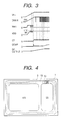
- FIG. 3 is timing charts showing a start timing of the switching regulator in the first embodiment
- FIG. 4 is a diagram showing the top view of a model of the driving power IC in the first embodiment
- FIG. 5 is a diagram showing the cross section of the model of the driving power IC in the first embodiment
- FIG. 6 is a diagram showing an equivalent circuit of the driving power IC in the first embodiment
- FIG. 7 is a diagram showing a cross section of the driving power IC's portion including a transistor serving as a main switch;
- FIG. 8 is a diagram showing a cross section of the driving power IC's portion including a starter switch and a start resistor;
- FIG. 9 is a diagram showing graphs each representing a characteristic of a resistor element used as the start resistor in the first embodiment
- FIG. 10 is diagram showing graphs each representing a characteristic of the resistor element in the first embodiment
- FIG. 11 is a diagram showing a model representing a case in which the driving power IC in the first embodiment is embedded monolithically into a control IC of a switching modulator;
- FIG. 12 is a diagram showing the cross section of a model of main elements in a state with FLRs and a field insulation layer formed on the surface of a semiconductor substrate in a process of manufacturing the driving power IC in the first embodiment;
- FIG. 13 is a diagram showing the cross section of a model of main elements in a state where the gate electrode of a transistor and a poly-silicon layer serving as the resistor layer of the resistor element are formed in a process of manufacturing the driving power IC in the first embodiment;
- FIG. 14 is a diagram showing the cross section of a model of main elements in a state with the gate electrode and the source area of a transistor and as well as the resistor layer formed in a process of manufacturing the driving power IC in the first embodiment;
- FIG. 15 is a diagram showing the cross section of a model of main elements in a state with an interlayer insulation film and contact holes formed in a process of manufacturing the driving power IC in the first embodiment
- FIG. 16 is a diagram showing the cross section of a model of main elements in a state with a protection insulation film formed in a process of manufacturing the driving power IC in the first embodiment
- FIG. 17 is a diagram showing of a model representing a first modified version of the resistor layer in the driving power IC in the first embodiment
- FIG. 18 is a diagram showing of a model representing a second modified version of the resistor layer in the driving power IC in the first embodiment
- FIG. 19 is a diagram showing of a model representing a third modified version of the resistor layer in the driving power IC in the first embodiment
- FIG. 20 is a diagram showing of a model representing a fourth modified version of the resistor layer in the driving power IC in the first embodiment
- FIG. 21 is a diagram showing of a model representing a fifth modified version of the resistor layer in the driving power IC in the first embodiment
- FIG. 22 is a diagram showing of a model representing a sixth modified version of the resistor layer in the driving power IC in the first embodiment
- FIG. 23 is a diagram showing of a model representing a seventh modified version of the resistor layer in the driving power IC in the first embodiment
- FIG. 24 is a diagram showing a model of a starter switch and a start resistor portion, which are in a second embodiment of the present invention.
- FIG. 25 is a diagram showing the top view of a model representing the resistor element in the second embodiment of the present invention and cross sections of portions of the resistor element;
- FIG. 26 ( a ) is a diagram showing a top view of a start resistor of a semiconductor device used as a driving power IC as proposed by the inventor of the present invention
- FIG. 26 ( b ) is a diagram showing a cross section of the start resistor
- FIG. 26 ( c ) is a diagram showing electric potentials at portions of the start resistor;
- FIG. 27 is a diagram showing graphs used for comparing states of deterioration in the proposed driving power IC.
- FIG. 28 is a diagram showing a withstand-voltage measuring circuit.
- FIGS. 1 to 16 are each a diagram in accordance with a first embodiment of the present invention.
- a semiconductor apparatus implemented by the first embodiment is configured as a driving power IC of a switching regulator.
- the driving power IC comprises a main switch MS and a starter circuit for starting the main switch MS.
- the starter circuit comprises a starter switch SS and a start resistor (a resistor element) SR.
- the main switch MS is implemented by MISFETs (or MOSFETs) while and the starter switch SS is implemented by a MISFET (or a MISFET).
- the start resistor SR has a sheet-resistance value of 10 k ⁇ / ⁇ , suppressing an increase in amount of dissipated heat.
- the start resistor SR is also created into a zigzag shape to increase its length and its area of heat dissipation. As a result, it is possible to a void a damage caused by heat dissipated by the poly-silicon layer used as a resistor layer.
- FIG. 2 is a diagram showing a switching-regulator circuit including an embedded driving power IC in the first embodiment. Only important components of the circuit are explained as follows.
- a full-wave rectification circuit is created between an input terminal receiving an alternating-current commercial power supply of typically 240 V and the primary coil 41 of a transformer 40 .
- the full-wave rectification circuit comprises a diode bridge rectification circuit 42 and a smoothing capacitor 43 .
- the secondary coil 44 of the transformer 40 is connected to a half-wave rectification circuit comprising a diode 45 and a smoothing capacitor 46 .
- the half-wave rectification circuit outputs a direct-current voltage through an output terminal.
- the primary coil 41 is connected to a drain pin of a control IC serving as pulse-width control circuit 50 .
- the pulse-width control circuit 50 has a power-supply (VDD) pin, a source pin, a comparator (COMP) pin, a capacitor-of-timing (CT) pin and a feedback (EB) pin.
- VDD power-supply
- COMP comparator
- CT capacitor-of-timing
- EB feedback
- a main switch MS is connected between the drain and source pins.
- a start resistor SR is connected between the gate electrode of a starter switch SS and the drain pin.
- the start resistor SR and the starter switch SS constitute a starter circuit. When a voltage appearing at the drain pain increases to a certain degree, the operation of the starter circuit is commenced.
- the output electrode of the starter switch SS is connected to a UVL (Under Voltage Lockout) circuit.
- the UVL circuit is connected to a UVL switch wired to the gate electrode of the starter switch SS. When the UVL circuit operates, the UVL switch is actuated to turn off the starter switch SS.
- An embedded oscillator (Osc.) is connected to the CT pin.
- An embedded error amplifier (E-AMP) is connected between the FB and COMP pins.
- a signal output by the error amplifier and a detection signal CS generated by the main switch MS are supplied to a comparison amplifier (C-AMP).
- the detection signal CS flows to a resistor RCS as a current, being converted into a voltage.
- a backup output voltage approximately equal to a voltage appearing at the VDD pin is supplied to the FB pin connected to the error amplifier as a feedback signal.
- Signals output by the oscillator and the comparison amplifier are supplied to a flip-flop circuit (FF).
- a signal generated by the flip-flop circuit is supplied to the gate electrode of the main switch MS to turn the main switch MS on or off.
- the VDD pin of the pulse-width control circuit 50 is connected to a backup power-supply circuit.
- the backup power-supply circuit comprises a diode Dc, a resistor Rc and a capacitor Cc which are connected in series to a tertiary coil (backup coil) 47 of the transformer 40 .
- a direct-current voltage is applied to the primary coil 41 , an electric-potential-charging circuit builds up an electric potential on the capacitor Cc as follows.
- the starter circuit employed in the pulse-width control circuit 50 operates to electrically charge the capacitor Cc.
- the operation to electrically charge the capacitor Cc continues and, as the voltage of the capacitor Cc reaches a release voltage, the UVL circuit operates, turning on the UVL switch.
- the starter switch SS With the UVL switch turned on, the starter switch SS is turned off and an operation to turn the main switch MS on and off is started. In the mean time, a voltage is induced in the backup coil 47 , the voltage serves as a power supply, and the operation of the pulse-width control circuit 50 is continued.
- a characteristic of the backup output voltage technique adopted in this fly-back system makes use of a property exhibiting the fact that the backup output voltage is proportional to a ratio of the number of turns in the backup coil 47 to the number of turns in the primary coil 41 of the transformer 40 and that the secondary output voltage is proportional to a ratio of the number of turns in the secondary coil 44 to the number of turns in the primary coil 41 of the transformer 40 .
- a pulse duty is controlled by adjusting the current detection level of the power MOSFET in accordance with the output terminal voltage of the error amplifier.
- FIG. 3 is timing charts showing a start timing of the switching regulator in the first embodiment. To be more specific, FIG. 3 shows variations in voltage of Vb + , DRAIN, Istart, VDD, CT, COMP and direct-current OUTPUT.
- Vb ⁇ is a voltage obtained as a result of rectification by the full-wave rectification circuit.
- the 240-VAC input of the commercial power supply is rectified to yield the voltage Vb + which is controlled by operating the pulse-width control circuit 50 in accordance with the start timing shown in FIG. 3 to produce a predetermined direct-current voltage.
- FIG. 2 also shows a typical waveform of the voltage appearing on the drain pin of the pulse-width control circuit 50 .
- FIG. 4 is a diagram showing the top view of a model of the semiconductor device in the first embodiment. To be more specific, the figure shows the top view of a model of the driving power IC monolithically created on a silicon semiconductor substrate 1 and composed of a main switch MS, a starter switch SS and a start resistor SR which constitute a high-voltage unit of a switching regulator.
- the inner side of a periphery area is used as an active area in which the main switch MS and the starter switch SS are created.
- a field insulation film 3 is provided between the periphery area and these MS & SS switches.
- a plurality of FLRs 13 are provided, enclosing the active area in a multiplexed state.
- the start resistor (resistor element) SR extends in a direction from a start edge on the inner side of the group of said multiplexed FLRs 13 to an end edge on the outer side of the group of said multiplexed FLRs 13 .
- FIG. 6 is a diagram showing an equivalent circuit of the driving power IC in the first embodiment.
- the driving power IC has 6 pins 1 to 6 .
- Pin 1 is a first pain or a drain pin outputting a signal.
- Pin 2 is a gate pin serving as a control pin.
- Pin 3 is a second pin or a source pin to which a reference electric potential GND is supplied.
- Pin 4 is s current-sensing (CS) pin.
- Pin 5 is a starter-circuit second pin (start-MOS source pin) for starting a control circuit.
- Pin 6 is a starter-circuit control pin (start-MOS gate pin).
- the main switch MS and the starter switch SS are configured as vertical MISFETs (MOSFETs) and a MISFET (MOSFET) respectively.
- MOSFETs vertical MISFETs
- MOSFET MISFET
- Each of the MISFETs (MOSFETs) comprises a number of cells.
- the cell structure is typically a mesh-gate structure.
- the main switch MS comprises a main MOS consisting of 2,270 cells and a 2-cell current-sensing (CS) MOS for detecting a current even though the structure of the main switch MS is not limited this configuration.
- a drain electrode (or a first electrode) of the main MOS is connected to the drain pin.
- a source electrode (or a second electrode) of the main MOS is connected to the source pin.
- a source electrode of the CS MOS is connected to the CS pin.
- a gate electrode of the main switch MS is connected to the gate pin.
- the starter switch SS is a start MOS comprising 60 cells even though the structure of the starter switch SS is not limited this configuration.
- a starter-switch drain electrode (or a starter-switch first electrode) of the start MOS is connected to the drain pin.
- a starter-switch source electrode (or a starter-switch second electrode) of the start MOS is connected to a start-MOS source pin.
- a starter-switch gate electrode of the starter switch SS is connected to a start-MOS gate pin.
- a start resistor SR having a resistance value of 2 M ⁇ is connected between the drain pin and the starter-switch gate electrode of the starter switch SS.
- FIG. 5 is a diagram showing the cross section of the model of the driving power IC in the first embodiment.
- FIG. 7 is a diagram showing a cross section of the driving power IC's portion including a transistor serving as a main switch MS.
- FIG. 8 is a diagram showing a cross section of the right half of the driving power IC's portion including the starter switch SS and the start resistor SR.
- the main surface of a semiconductor substrate made of n + silicon includes an n ⁇ epitaxial layer 2 .
- the main switch MS and the starter switch SS are formed sequentially by selectively doping the n ⁇ epitaxial layer 2 with predetermined impurities. That is, a plurality of cells each having a planar structure are laid out regularly over an active area. Gates 5 of adjacent cells provided on a gate insulation film 4 formed on the main surface are connected to each other to create a mesh gate structure wherein the cells are connected in parallel.
- the gates 5 of cells on a circumference are connected to a gate wire 6 made of typically poly-silicon on the periphery of the cell area.
- the gate wire 6 is connected to a gate pad which is a connection area of the gates 5 .
- the cells over the n ⁇ epitaxial layer 2 cover a MOSFET's drain area, base area and source area.
- a p layer 7 created on the main surface of the semiconductor substrate 1 forms a channel in the base area.
- the source area is an n + layer 8 created on the p layer 7 .
- the MOSFET is a FET with a vertical structure. Since the semiconductor substrate 1 serves as a drain, a drain electrode is formed on the entire back surface of the semiconductor substrate 1 as shown in none of the figures.
- the drain electrode is created as a stacked-layer film comprising stacked layers each made of typically nickel, titan, nickel and silver respectively.
- the gate wire 6 protrudes to an upper layer through an interlayer insulation film 9 , being electrically connected to a gate guard ring 10 made of typically aluminum including silicon.
- An n + layer 8 serving as a source is electrically connected to a source wire 11 made of typically aluminum including silicon.
- the source wire 11 is created over the interlayer insulation film 9 on the main surface of the semiconductor substrate 1 .
- the n + layer 8 serving as a source is also electrically connected to a p + contact layer 12 provided on the p layer 7 in order to keep an electrical potential of the base at a fixed level.
- a plurality of concentric field limiting rings (FLRs) 13 are provided.
- Each of the FLRs 13 is formed along a circumference of the semiconductor substrate 1 and has a rectangular-ring-like shape with the corners thereof each forming an arc.
- the FLRs 13 are each made of a p diffusion layer.
- the FLRs 13 constitute a structure wherein, as a voltage applied thereto increases, a punch-through depletion layer is built, extending in a direction from an inner-circumference one of the FLRs 13 to an outer-circumference one thereof prior to occurrence of an avalanche breakdown and, eventually, a breakdown occurs at a junction portion of the FLR 13 on the outermost circumference.
- the withstand voltage of the power MISFET is set at a value in the range 750 V to 800 V. For this reason, the withstand voltage of an FLR 13 is set at at least 800 V.
- the breakdown voltage of an FLR 13 is logically the sum of a punch-through withstand voltage between the FLRs 13 and the breakdown voltage of the ring on the outermost circumference, the breakdown voltage of an FLR 13 can be increased by raising the number of FLRs 13 .
- the number of FLRs 13 is determined by taking a termination length into consideration. While the number of FLRs 13 is 5 in FIG. 1 and the number of FLRs 13 is 4 in other figures, these numbers are typical to the bitter end.
- the start resistor SR is created on a portion of the field insulation film 3 formed earlier.
- the resistor layer 20 serving as the start resistor (resistor element) SR extends in a direction from a start edge 31 on the inner side of the group of said FLRs 13 to an end edge 32 on the outer side of the group of said FLRs 13 .
- the start resistor SR is formed into a zigzag shape to increase its length and, hence, its heat-dissipating area and to improve its heat-dissipation characteristic.
- five FLRs 13 namely, P 1 to P 5 , are created even though the number of FLRs is not limited to 5.
- FIG. 1 ( a ) is a diagram showing a model of a zigzag pattern of a resistor layer serving as the start resistor (resistor element) SR.
- FIG. 1 ( b ) is a diagram showing a cross section of the driving power IC's portion including the FLRs and the resistor layer.
- FIG. 1 ( c ) is a diagram showing graphs representing electric potentials appearing at portions of the resistor layer and the semiconductor substrate's surface including the FLRs.
- the field limiting rings (FLRs) 13 denoted by reference notations P 1 to P 5 are each created from a p diffusion layer on the surface of an epitaxial layer 2 in a periphery area in a direction from an active area not shown in the figure to the periphery area to enclose the active area. It should be noted that, on the inner side of the FLR P 1 , a p diffusion layer P 0 is created, being held at a ground electric potential (GND)
- a guard ring 14 is provided on the edge of the semiconductor chip.
- the guard ring 14 is created on the surface of the n ⁇ epitaxial layer 2 beneath an insulation film 24 thinner than the field insulation film 3 at a location outside the field insulation film 3 .
- the guard ring 14 is formed in a n + diffusion area with a ring shape by diffusing impurities into the main surface of the n ⁇ epitaxial layer 2 at a high concentration.
- a resistor layer 20 made of a poly-silicon layer is provided on the field insulation film 3 .
- the surface of the resistor layer 20 is covered by the interlayer insulation film 9 .
- a contact hole 21 is formed by boring a location on the interlayer insulation film 9 above the p diffusion layer P 0 and a contact hole 22 is formed by boring a periphery location on the interlayer insulation film 9 .
- a contact hole 23 is formed at a location outside the edge of the field insulation film 3 .
- the contact hole 23 is extended to a location outside the insulation film 24 , which is thinner than the field insulation film 3 and provided at a location separated away from the field insulation film 3 as described above.
- Conductor films 25 to 28 each having a ring shape are created along the periphery of the semiconductor chip on the interlayer insulation film 9 .
- the conductor film 25 is created on the inner side of the periphery area, that is, on the active-area side of the periphery area.
- the conductor film 25 also fills up the contact hole 21 , being electrically connected to the resistor layer 20 .
- the conductor film 26 is created at a location adjacent to the conductor film 25 on the outer side of the conductor film 25 and is electrically connected to the p diffusion layer P 0 held at the ground electric potential GND used as a reference electric potential.
- the conductor film 27 is created above the FLR 13 on the outermost circumference or the layer P 5 , being electrically connected to the FLR 13 .
- the conductor film 28 also fills up the contact holes 22 and 23 and is electrically connected to the resistor layer 20 and the guard ring 14 .
- the withstand voltage of the start resistance SR is equal to the sum of the withstand voltage of the portion comprising the FLRs 13 and a withstand voltage due to, among other factors, the thickness of the field insulation film 3 .
- the start resistance SR has a total withstand voltage of at least 800 V.
- a resistor-layer portion corresponding to the contact hole 21 is the start edge 31 of the resistor element serving as the start resistor SR and a resistor-layer portion corresponding to the contact hole 22 is the end edge 32 of the start resistor SR.
- a pattern of the resistor layer 20 serving as the resistance SR starting from the start edge 31 and ending at the end edge 32 displays a zigzag shape which has a fixed amplitude and changes the direction at fixed pitch intervals as shown in FIG. 1 ( a ). In FIG. 1 ( b ), however, the zigzag shape is not explicitly shown for the sake of simplicity.
- the resistor layer 20 By forming the resistor layer 20 into a zigzag pattern as described above, the length of the resistor layer 20 increases, resulting in a greater heat-dissipating area.
- the sheet resistance of the resistor layer 20 by setting the sheet resistance of the resistor layer 20 at 10 k ⁇ / ⁇ , the amount of dissipated heat at a certain voltage can be set at a fixed value. As a result, it is possible to avoid destruction caused by fusion of the poly-silicon layer serving as the resistor layer due to dissipated heat.
- the resistor layer 20 is designed to into a flattened shape in order to increase the surface area relative to a cross-sectional area by taking heat dissipation into consideration.
- the resistor layer 20 is made of typically a poly-silicon layer doped with n-conduction impurities such as phosphor and p-conduction impurities such as boron for adjusting the resistance value or the sheet resistance.
- the present invention prevents the strength to withstand a voltage from deteriorating by making electric potentials appearing at portions of a hypothetical equivalent segment resistor having the shape of a straight line connecting the start and end edges of the resistor element SR and electric potentials appearing at portions on the surface of a semiconductor substrate which correspond to the portions of the segment resistor agree with each other, or making the latter potentials approximately close to the former potentials.
- the material (or the sheet resistance), the pattern, the width and the thickness of a resistor layer serving as a resistor element are changed and the thickness of a field insulation film are varied so as to make electric potentials appearing at portions of a hypothetical equivalent segment resistor having the shape of a straight line connecting the start and end edges of the resistor element SR and electric potentials appearing at portions on the surface of a semiconductor substrate which correspond to the portions of the segment resistor agree with each other.
- the first embodiment has a configuration wherein the zigzag pitch of the resistor layer 20 at some locations is made different from the rest.
- the zigzag pitch of the resistor layer 20 for area A is made greater than the zigzag pitch of the resistor layer 20 for area B where area A is an area between the start edge 31 and the FLR 13 on the outermost circumference and area B is an area between the end edge 32 and the FLR 13 on the outermost circumference as shown in FIG. 1 ( a ).
- straight lines e and f compose a curve representing electric potentials appearing at portions of a hypothetical equivalent segment resistor having the shape of a straight line connecting the start edge 31 and the end edge 32 of the resistor element as shown in FIG. 1 ( c ).
- the straight line e having a moderate gradient represents electric potentials appearing in area A between the start edge 31 and the FLR 13 on the outermost circumference.
- the straight line f having a gradient more abrupt than the slope of the straight line e represents electric potentials appearing in area B between the end edge 32 and the FLR 13 on the outermost circumference.
- the straight lines e and f coincide with a curve d at some locations and approach the curve f at other locations where the curve d represents electric potentials appearing on the surface of the semiconductor substrate.
- the difference in electric potential between areas A & B and the surface of the semiconductor substrate can be reduced to a level below about typically 50 V at a location where the straight line e or f is separated from the curve f even if a high voltage is applied. As a result, it is possible to avoid a damage caused by a strong electric field of the field insulation film.
- a location at which a strong magnetic field is generated is the location of the FLR 13 placed on the outermost circumference and denoted by reference notation P 5 .
- the electric potential of the resistor element at the location of the FLR 13 (P 5 ) agrees with the electric potential appearing on the surface of the semiconductor substrate, it is possible to make electric potentials appearing at portions of a hypothetical equivalent segment resistor having the shape of a straight line connecting the start and end edges of the resistor element SR agree with electric potentials appearing at portions on the surface of a semiconductor substrate which correspond to the portions of the segment resistor, or to make the latter potentials approximately close to the former potentials. That is, the resistance value per unit length of the segment on the outer side of the FLR 13 on the outermost circumference is made different from the resistance value per unit length of the segment on the inner side of the FLR 13 on the outermost circumference.
- the sheet resistance of the resistor layer 20 is made small to avoid breakage caused by thermal fusion.
- the sheet resistance of the resistor layer 20 is made small to prevent the amount of dissipated heat from increasing and, furthermore, the resistor layer 20 is designed into a zigzag shape to increase the length and, hence, the area of thermal dissipation so that breakage caused by thermal fusion can be avoided.
- FIG. 9 is a diagram showing graphs each representing a voltage versus current characteristic of the start resistor created at different resistance sheets in accordance with the first embodiment.
- the resistance value decreases due to heat dissipated by the resistor element.
- it is necessary to reduce the sheet resistance to a value not exceeding 10 k ⁇ / ⁇ .
- FIG. 10 is diagram showing graphs each representing a temperature versus sheet-resistance characteristic of the resistor element created at different impurity concentrations in accordance with the first embodiment.
- a resistor element having a large sheet resistance has a negative temperature characteristic.
- the greater the sheet resistance the greater the variation in resistance caused by a change in temperature.
- this embodiment implements a semiconductor device wherein the high-voltage unit of the switching regulator is implemented as an integrated circuit and the control circuit is put in another chip.
- the present invention can also be applied to a semiconductor device of a switching regulator with the control circuit integrated therein as shown in FIG. 11 .
- FIGS. 12 to 16 a method of manufacturing the driving power IC (or the semiconductor device) is explained by referring to FIGS. 12 to 16 .
- a MOSFET portion is shown on the left side while a resistor-element (start-resistor) portion created in the same process is shown on the right side.
- an n ⁇ epitaxial layer 2 is created by using an epitaxial-growth technique on an n + semiconductor substrate 1 made of monolithic silicon with arsenic (As) or the like injected therein. Then, a plurality of FLRs 13 are created in the periphery area of the n ⁇ epitaxial layer 2 , enclosing an active area of the semiconductor chip by multiplexing p wells, and a silicon-oxide film is formed on the main surface of the semiconductor substrate 1 by adoption of typically a thermal oxidation method. A mask of a silicon-nitride (SiN) is then created on the silicon-oxide film. Subsequently, the field insulation film 3 is formed by selective thermal oxidation with the silicon-nitride film used as a mask. A state after the formation of the field insulation film 3 is shown in FIG. 12 .
- SiN silicon-nitride
- the gate insulation film 4 is created on the main surface of the semiconductor substrate 1 by stacking thermal-oxide films or silicon-oxide films on a thermal-oxide film by adoption of a CVD (Chemical Vapor Deposition) technique.
- a poly-silicon film 5 ′ to serve as a conductor film of the resistor element SR and to serve as a gate 5 is created on the entire main surface of the semiconductor substrate 1 by using the CVD technique.
- phosphor is introduced in an area of the poly-silicon film 5 ′ to serve as the gate 5 .
- boron is introduced in an area of the poly-silicon film 5 ′ to serve as the conductor film of the resistor element SR. A state at the end of this process is show in FIG. 13 .
- the poly-silicon film 5 ′ is selectively etched in a patterning process to form the gate 5 and the resistor layer 20 of the element SR.
- the MISFET's p layer 7 , n + layer 8 and contact layer 12 are created by ion injection using a mask in a photolithography process.
- a p + layer is created for reducing the contact-resistance values of the conductor film of the element SR.
- an n + layer is created instead of creating a p + layer. A state at the end of this process is shown in FIG. 14 .
- a predetermined mask is used to create the resistor film 20 with a zigzag pitch varying at the FLR 13 on the outermost circumference as shown in FIG. 1 ( a ).
- the interlayer insulation film 9 is created by formation of an SOG (Spin On Glass) film in a coating process. Holes are created by boring through the interlayer insulation film 9 , being exposed to an n + layer 8 to serve as a source area, a gate wire 6 and a connection area of the element SR. A state at the end of the process is shown in FIG. 15 .
- a conductor film or a metallic film is created on the semiconductor substrate's entire main surface including the insides of these holes.
- the conductor film is made of typically aluminum including silicon.
- this metallic film is subjected to a patterning process to form a gate guard ring 10 , a source wire 11 and a guard ring 14 .
- the silicon-oxide film is coated with polyimid stacked on the film as a layer by adoption of a plasma CVD technique using typically tetraethoxyline (TEOS) gas mainly as the source gas, and a protection insulation film 15 is created for covering the entire main surface of the semiconductor substrate 1 .
- TEOS typically tetraethoxyline
- the back surface of the n + semiconductor substrate 1 is polished before creation of a drain electrode 16 by sequentially stacking nickel, titan, nickel and silver layers on the back surface through adoption of a deposition technique. A state at the end of this process is shown in FIG. 16 .
- the start resistor (or the resistor element) SR can be formed by utilizing the process to create the main switch MS and the starter switch SS during the manufacture, the number of processes does not increase.
- the start resistor SR is not provided in the active area but created on the field insulation film, the size of the driving power IC can be reduced.
- the resistor element in the present invention, it is desirable to manufacture the element so that electric potentials appearing at portions of a hypothetical equivalent segment resistor having the shape of a straight line connecting the start and end edges of the resistor element SR agree with electric potentials appearing at portions on the surface of a semiconductor substrate which correspond to the portions of the segment resistor.
- FIG. 17 is a diagram showing of a model representing a first modified version of the resistor layer in the driving power IC in the first embodiment.
- the zigzag width of the zigzag pattern is fixed throughout the resistor element from the start edge 31 to the end edge 32 .
- the zigzag pitch of the resistor layer 20 for area A is made greater than the zigzag pitch of the resistor layer 20 for area B where area A is an area between the start edge 31 and the FLR 13 (P 5 ) the outermost circumference and area B is an area between the end edge 32 and the FLR 13 (P 5 ) on the outermost circumference.
- the resistor-layer width or the resistor-line width of the resistor layer 20 for area A is made greater than the resistor-layer width of the resistor layer 20 for area B.
- FIG. 18 is a diagram showing of a model representing a second modified version of the resistor layer in the driving power IC in the first embodiment.
- the zigzag width and the zigzag pitch of the zigzag pattern are fixed throughout the resistor element from the start edge 31 to the end edge 32 .
- the sheet resistance on the outer side of the FLR 13 (P 5 ) on the outermost circumference is made different from the sheet resistance on the inner side of the FLR 13 (P 5 ).
- the sheet resistance of the resistor layer 20 on the inner side is made low while the sheet resistance of the resistor layer 20 on the outer side is made high.
- the strength to withstand a voltage can be prevented from deteriorating due to a strong electric field.
- FIG. 19 is a diagram showing of a model representing a third modified version of the resistor layer in the driving power IC in the first embodiment.
- the zigzag pitch is uniform over the entire resistor element from the start edge 31 to the end edge 32 but the zigzag width on the outer side of the FLR 13 (PS) on the outermost circumference is made different from the zigzag width on the inner side of the FLR 13 (P 5 ).
- the zigzag width of the resistor layer 20 on the inner side is made small while the zigzag width of the resistor layer 20 on the outer side is made large.
- the strength to withstand a voltage can be prevented from deteriorating due to a strong electric field.
- FIG. 20 is a diagram showing of a model representing a fourth modified version of the resistor layer in the driving power IC in the first embodiment.
- the zigzag pitch on the outer side of the FLR 13 (P 5 ) on the outermost circumference is made different from the zigzag pitch on the inner side of the FLR 13 (PS), and the zigzag width on the outer side is becoming smaller gradually so that the electric potentials appear on the surface of the semiconductor substrate 1 between the end edge 32 and the FLR 13 (P 5 ) on the outermost circumference as shown by the curve d in FIG. 1 ( c ).
- the strength to withstand a voltage can be prevented from deteriorating due to a strong electric field.
- FIG. 21 is a diagram showing of a model representing a fifth modified version of the resistor layer in the driving power IC in the first embodiment.
- a pattern of the resistor element is designed so that, in the area between the start edge 31 and the FLR 13 (PS) on the outermost circumference, the resistor element has a straight-line shape with electric potentials represented by the straight line e having a moderate slope as shown in FIG. 1 ( c ) and, in the area between the end edge 32 and the FLR 13 (P 5 ) on the outermost circumference, the resistor element has a zigzag shape.
- the strength to withstand a voltage can be prevented from deteriorating due to a strong electric field.
- FIG. 22 is a diagram showing of a model representing a sixth modified version of the resistor layer in the driving power IC in the first embodiment.
- a pattern of the resistor element is designed so that, in the area between the start edge 31 and the end edge 32 , the resistor element has a straight-line shape.
- the width of the resistor layer 20 in an area between the start edge 31 and the FLR 13 (P 5 ) on the outermost circumference is made large while the width of the resistor layer 20 in an area between the end edge 32 and the FLR 13 (P 5 ) on the outermost circumference is made small.
- FIG. 23 is a diagram showing of a model representing a seventh modified version of the resistor layer in the driving power IC in the first embodiment.
- a pattern of the resistor element is designed so that, in the area between the start edge 31 and the end edge 32 , the resistor element has a straight-line shape with a fixed resistor-layer width.
- the sheet resistance of the resistor layer 20 in the area between the end edge 31 and the FLR 13 (PS) on the outermost circumference is made small while the sheet resistance of the resistor layer 20 in the area between the end edge 32 and the FLR 13 (P 5 ) on the outermost circumference is made large.
- the resistor layer 20 is created by:
- the resistor layer 20 can also be created during creation of the gate electrode from poly-silicon in the process of manufacturing the MOSFET.
- the sheet resistance can be adjusted by the quantity of the added impurities.
- the resistor layer 20 can also be made of different materials in its longitudinal direction. For example, a metallic wire and a poly-silicon layer can be used at some locations in the longitudinal direction of the resistor layer 20 .
- the thickness of the field insulation film can be increased to a value in the range 3 to 5 ⁇ m over the conventional thickness of about 1.5 ⁇ m in order to make electric potentials appearing at portions of a hypothetical equivalent segment resistor having the shape of a straight line connecting the start and end edges of the resistor element SR agree with electric potentials appearing at portions on the surface of a semiconductor substrate which correspond to the portions of the segment resistor.
- the sheet resistance of the resistor layer serving as the start resistor is set at a low value of 10 k ⁇ / ⁇ , the amount of dissipated heat can be made constant.
- the resistor layer by forming the resistor layer into a zigzag shape, it is possible to increase the length of the resistor layer. With the length increased, the area dissipating heat is widened so that the heat dissipation efficiency is also raised. As a result, it is possible to avoid a destruction incident caused by fusion of the poly-silicon layer serving as the resistor layer due to dissipated heat.
- the size of the semiconductor chip can be made small and the cost to manufacture the semiconductor device can be reduced in comparison with a structure in which the start resistor is created in an active area.
- FIGS. 24 and 25 are each a diagram relevant to another embodiment of the present invention, namely, the second embodiment.
- FIG. 24 is a diagram showing a model of a starter switch and a start resistor portion, which are provided by a second embodiment of the present invention.
- FIG. 25 is a diagram showing the top view of a model representing the resistor element in the second embodiment of the present invention and cross sections of portions of the resistor element.
- the driving power IC has a configuration in which the FLRs 13 are electrically connected to the resistor layer 20 as shown in FIG. 24 .
- FIG. 24 is a conceptual diagram which shows that direct contact holes are formed through the field insulation film 3 at locations beneath the resistor layer 20 and portions of the field insulation film 3 are embedded in the contact holes, being electrically connected to the FLRs 13 . Since the field insulation film 3 is thick, however, fine fabrication is difficult. Thus, in actuality, the contact holes are formed on portions where thin films exist at locations where the interlayer insulation film 9 and the FLRs 13 extend as shown in FIG. 25.
- a wire 17 is provided in an area between contact holes and an area including the contact holes. The wire 17 is used for electrically connecting a FLR 13 and a portion of the start resistor corresponding to the FLR 13 .
- FIG. 25 is a diagram showing the top view of a model representing the resistor element used as the start resistor SR.
- Cross sections indicated by reference notations A-A′, B-B′ and C-C′ on the left side are shown on the right side of FIG. 25 .
- each of FLRs 13 is electrically connected to a corresponding portion of the resistor layer 20 so as to provide equal electric potentials to the FLR 13 and the portion.
- electric potentials appearing at portions of a hypothetical equivalent segment resistor having the shape of a straight line connecting the start edge 31 and the end edge 32 of the resistor element (start resistor) SR agree with electric potentials appearing at portions on the surface of a semiconductor substrate which correspond to the portions of the segment resistor, or the latter potentials are approximately close to the former potentials.
- the strength to withstand a voltage can be prevented from deteriorating.
- the sheet resistance of the resistor layer serving as the start resistor is set at a low value of 10 k ⁇ / ⁇ , the amount of dissipated heat can be made almost constant.
- the resistor layer by forming the resistor layer into a zigzag shape, it is possible to increase the length of the resistor layer. With the length increased, the area dissipating heat is widened so that the heat dissipation efficiency is also raised. As a result, it is possible to avoid a destruction incident caused by fusion of the poly-silicon layer serving as the resistor layer due to dissipated heat.
- the size of the semiconductor chip can be made small and the cost to manufacture the semiconductor device can be reduced in comparison with a structure in which the start resistor is created in an active area.
Abstract
Description
Claims (18)
Applications Claiming Priority (2)
| Application Number | Priority Date | Filing Date | Title |
|---|---|---|---|
| JP2000130705A JP4024990B2 (en) | 2000-04-28 | 2000-04-28 | Semiconductor device |
| JP2000-130705 | 2000-04-28 |
Publications (2)
| Publication Number | Publication Date |
|---|---|
| US20010035554A1 US20010035554A1 (en) | 2001-11-01 |
| US6492689B2 true US6492689B2 (en) | 2002-12-10 |
Family
ID=18639745
Family Applications (1)
| Application Number | Title | Priority Date | Filing Date |
|---|---|---|---|
| US09/842,015 Expired - Lifetime US6492689B2 (en) | 2000-04-28 | 2001-04-26 | Semiconductor device switching regulator used as a DC regulated power supply |
Country Status (3)
| Country | Link |
|---|---|
| US (1) | US6492689B2 (en) |
| JP (1) | JP4024990B2 (en) |
| KR (1) | KR100626786B1 (en) |
Cited By (10)
| Publication number | Priority date | Publication date | Assignee | Title |
|---|---|---|---|---|
| US20040235258A1 (en) * | 2003-05-19 | 2004-11-25 | Wu David Donggang | Method of forming resistive structures |
| US6989566B2 (en) * | 2001-06-04 | 2006-01-24 | Matsushita Electric Industrial Co., Ltd. | High-voltage semiconductor device including a floating block |
| US20060214894A1 (en) * | 2005-03-28 | 2006-09-28 | Wei-Chung Cheng | Power wiring structure and method for a plurality of driver chips on a display panel |
| US20070085135A1 (en) * | 2005-10-14 | 2007-04-19 | Mitsubishi Electric Corporation | Semiconductor device |
| US20080018389A1 (en) * | 2006-07-24 | 2008-01-24 | Samsung Electronics Co., Ltd. | Layout schemes and methods of power gating transistor switches, semiconductor devices including the power gating transistor switches, and power gating methods of the semiconductor devices |
| US20080117653A1 (en) * | 2006-11-20 | 2008-05-22 | Fuji Electric Device Technology Co., Ltd. | Semiconductor Device, Integrated Circuit Including the Semiconductor Device, Control IC for Switching Power Supply and the Switching Power Supply |
| US20110228575A1 (en) * | 2006-03-24 | 2011-09-22 | Fuji Electric Systems Co., Ltd. | Junction field effect transistor, integrated circuit for switching power supply, and switching power supply |
| US20130214394A1 (en) * | 2012-02-22 | 2013-08-22 | Toyota Jidosha Kabushiki Kaisha | Semiconductor device |
| US9401314B2 (en) | 2013-06-07 | 2016-07-26 | Mitsubishi Electric Corporation | Method of testing semiconductor device |
| US10388722B2 (en) * | 2016-10-25 | 2019-08-20 | Infineon Technologies Ag | Power semiconductor device termination structure |
Families Citing this family (20)
| Publication number | Priority date | Publication date | Assignee | Title |
|---|---|---|---|---|
| US6552597B1 (en) * | 2001-11-02 | 2003-04-22 | Power Integrations, Inc. | Integrated circuit with closely coupled high voltage output and offline transistor pair |
| JP2005268249A (en) * | 2004-03-16 | 2005-09-29 | Philtech Inc | Semiconductor device and its manufacturing method |
| JP4895104B2 (en) * | 2006-07-06 | 2012-03-14 | ルネサスエレクトロニクス株式会社 | Semiconductor device |
| JP4974653B2 (en) * | 2006-11-21 | 2012-07-11 | ローム株式会社 | Step-up switching regulator control circuit, step-up switching regulator using the same, and electronic equipment using them |
| US8897039B2 (en) * | 2007-06-12 | 2014-11-25 | Bcd Semiconductor Manufacturing Limited | Method and system for pulse frequency modulated switching mode power supplies |
| KR100887884B1 (en) * | 2007-10-01 | 2009-03-06 | 주식회사 동부하이텍 | Semiconductor device |
| US8638160B2 (en) | 2007-12-14 | 2014-01-28 | Fuji Electric Co., Ltd. | Integrated circuit and semiconductor device |
| TWM351555U (en) * | 2008-05-06 | 2009-02-21 | Bcd Semiconductor Mfg Ltd | Method and apparatus for reducing standby power of switching mode power supplies |
| US8125799B2 (en) * | 2009-10-23 | 2012-02-28 | Bcd Semiconductor Manufacturing Limited | Control circuits and methods for switching mode power supplies |
| JP2010239832A (en) * | 2009-03-31 | 2010-10-21 | Panasonic Corp | Current limiting circuit |
| US8045348B2 (en) * | 2009-04-09 | 2011-10-25 | Bcd Semiconductor Manufacturing Limited | Switching mode power supply controller with high voltage startup circuits |
| US8242013B2 (en) * | 2010-03-30 | 2012-08-14 | Alpha & Omega Semiconductor Inc. | Virtually substrate-less composite power semiconductor device and method |
| JP5575610B2 (en) * | 2010-11-09 | 2014-08-20 | 本田技研工業株式会社 | Power supply |
| US8482029B2 (en) * | 2011-05-27 | 2013-07-09 | Infineon Technologies Austria Ag | Semiconductor device and integrated circuit including the semiconductor device |
| CN102354703B (en) * | 2011-10-19 | 2013-01-23 | 扬州杰利半导体有限公司 | Planar structure-type superhigh-voltage diode chip |
| CN103746002B (en) * | 2013-12-17 | 2016-04-20 | 西安理工大学 | A kind of step groove-field limiting ring composite terminal structure |
| JP6099807B2 (en) * | 2014-03-06 | 2017-03-22 | 三菱電機株式会社 | Semiconductor device and test method thereof |
| US11509225B2 (en) * | 2017-09-28 | 2022-11-22 | Rohm Co., Ltd. | Power IC including a feedback resistor, and a switching power supply and electronic appliance including the power IC |
| DE102021117826A1 (en) | 2021-07-09 | 2023-01-12 | Infineon Technologies Ag | Power semiconductor device Method of manufacturing a power semiconductor device |
| CN117116915B (en) * | 2023-10-25 | 2024-01-19 | 合肥晶合集成电路股份有限公司 | Semiconductor structure, preparation method thereof and square resistance measuring method |
Citations (5)
| Publication number | Priority date | Publication date | Assignee | Title |
|---|---|---|---|---|
| US4707719A (en) * | 1984-11-21 | 1987-11-17 | U.S. Philips Corporation | Semiconductor device having an annular region for improved voltage characteristics |
| US5315139A (en) * | 1992-06-24 | 1994-05-24 | Kabushiki Kaisha Toshiba | Power semiconductor integrated circuit device without concentration of electric field |
| US5324971A (en) * | 1992-04-09 | 1994-06-28 | U.S. Philips Corporation | Power semiconductor device having over voltage protection |
| JPH09186315A (en) | 1995-12-28 | 1997-07-15 | Hitachi Ltd | Semiconductor device |
| US5903033A (en) * | 1996-11-29 | 1999-05-11 | Mitsubishi Denki Kabushiki Kaisha | Semiconductor device including resistance element with superior noise immunity |
Family Cites Families (3)
| Publication number | Priority date | Publication date | Assignee | Title |
|---|---|---|---|---|
| JPH0612654B2 (en) * | 1985-04-29 | 1994-02-16 | ソニー株式会社 | Built-in resistor of cathode ray tube |
| JP2850694B2 (en) * | 1993-03-10 | 1999-01-27 | 株式会社日立製作所 | High breakdown voltage planar type semiconductor device |
| JPH07297368A (en) * | 1994-04-25 | 1995-11-10 | Rohm Co Ltd | Resistor and semiconductor device |
-
2000
- 2000-04-28 JP JP2000130705A patent/JP4024990B2/en not_active Expired - Fee Related
-
2001
- 2001-04-26 US US09/842,015 patent/US6492689B2/en not_active Expired - Lifetime
- 2001-04-28 KR KR1020010023248A patent/KR100626786B1/en not_active IP Right Cessation
Patent Citations (5)
| Publication number | Priority date | Publication date | Assignee | Title |
|---|---|---|---|---|
| US4707719A (en) * | 1984-11-21 | 1987-11-17 | U.S. Philips Corporation | Semiconductor device having an annular region for improved voltage characteristics |
| US5324971A (en) * | 1992-04-09 | 1994-06-28 | U.S. Philips Corporation | Power semiconductor device having over voltage protection |
| US5315139A (en) * | 1992-06-24 | 1994-05-24 | Kabushiki Kaisha Toshiba | Power semiconductor integrated circuit device without concentration of electric field |
| JPH09186315A (en) | 1995-12-28 | 1997-07-15 | Hitachi Ltd | Semiconductor device |
| US5903033A (en) * | 1996-11-29 | 1999-05-11 | Mitsubishi Denki Kabushiki Kaisha | Semiconductor device including resistance element with superior noise immunity |
Non-Patent Citations (1)
| Title |
|---|
| IEEE Transactions on Electron Devices, vol. 44, No. 11, Nov. 1997, "Spiral Junction Termination", D. Krizaj et al, pp. 2002-2010. |
Cited By (18)
| Publication number | Priority date | Publication date | Assignee | Title |
|---|---|---|---|---|
| US6989566B2 (en) * | 2001-06-04 | 2006-01-24 | Matsushita Electric Industrial Co., Ltd. | High-voltage semiconductor device including a floating block |
| US20040235258A1 (en) * | 2003-05-19 | 2004-11-25 | Wu David Donggang | Method of forming resistive structures |
| US20060214894A1 (en) * | 2005-03-28 | 2006-09-28 | Wei-Chung Cheng | Power wiring structure and method for a plurality of driver chips on a display panel |
| US20070085135A1 (en) * | 2005-10-14 | 2007-04-19 | Mitsubishi Electric Corporation | Semiconductor device |
| US7560773B2 (en) * | 2005-10-14 | 2009-07-14 | Mitsubishi Electric Corporation | Semiconductor device |
| US9461115B2 (en) | 2006-03-24 | 2016-10-04 | Fuji Electric Co., Ltd. | Junction field effect transistor, integrated circuit for switching power supply, and switching power supply |
| US8283705B2 (en) | 2006-03-24 | 2012-10-09 | Fuji Electric Co., Ltd. | Junction field effect transistor, integrated circuit for switching power supply, and switching power supply |
| US20110228575A1 (en) * | 2006-03-24 | 2011-09-22 | Fuji Electric Systems Co., Ltd. | Junction field effect transistor, integrated circuit for switching power supply, and switching power supply |
| US7840926B2 (en) * | 2006-07-24 | 2010-11-23 | Samsung Electronics Co., Ltd. | Layout schemes and methods of power gating transistor switches, semiconductor devices including the power gating transistor switches, and power gating methods of the semiconductor devices |
| US20080018389A1 (en) * | 2006-07-24 | 2008-01-24 | Samsung Electronics Co., Ltd. | Layout schemes and methods of power gating transistor switches, semiconductor devices including the power gating transistor switches, and power gating methods of the semiconductor devices |
| US20090323376A1 (en) * | 2006-11-20 | 2009-12-31 | Fuji Electric Device Technology Co., Ltd. | Semiconductor device, integrated circuit including the semiconductor device, control ic for switching power supply and the switching power supply |
| US20080117653A1 (en) * | 2006-11-20 | 2008-05-22 | Fuji Electric Device Technology Co., Ltd. | Semiconductor Device, Integrated Circuit Including the Semiconductor Device, Control IC for Switching Power Supply and the Switching Power Supply |
| US8680622B2 (en) | 2006-11-20 | 2014-03-25 | Fuji Electric Co., Ltd. | Semiconductor device, integrated circuit including the semiconductor device, control IC for switching power supply and the switching power supply |
| US8860145B2 (en) | 2006-11-20 | 2014-10-14 | Fuji Electric Co., Ltd. | Semiconductor device, integrated circuit including the semiconductor device, control IC for switching power supply and the switching power supply |
| US20130214394A1 (en) * | 2012-02-22 | 2013-08-22 | Toyota Jidosha Kabushiki Kaisha | Semiconductor device |
| US9048085B2 (en) * | 2012-02-22 | 2015-06-02 | Toyota Jidosha Kabushiki Kaisha | Semiconductor device |
| US9401314B2 (en) | 2013-06-07 | 2016-07-26 | Mitsubishi Electric Corporation | Method of testing semiconductor device |
| US10388722B2 (en) * | 2016-10-25 | 2019-08-20 | Infineon Technologies Ag | Power semiconductor device termination structure |
Also Published As
| Publication number | Publication date |
|---|---|
| US20010035554A1 (en) | 2001-11-01 |
| KR100626786B1 (en) | 2006-09-22 |
| KR20010098965A (en) | 2001-11-08 |
| JP4024990B2 (en) | 2007-12-19 |
| JP2001313367A (en) | 2001-11-09 |
Similar Documents
| Publication | Publication Date | Title |
|---|---|---|
| US6492689B2 (en) | Semiconductor device switching regulator used as a DC regulated power supply | |
| US11270993B2 (en) | MOSFET device of silicon carbide having an integrated diode and manufacturing process thereof | |
| US9634130B2 (en) | Semiconductor device | |
| US5321295A (en) | Insulated gate bipolar transistor and method of fabricating the same | |
| US8212282B2 (en) | Semiconductor device used in step-up DC-DC converter, and step-up DC-DC converter | |
| EP0566179B1 (en) | A semiconductor component including protection means | |
| US7642599B2 (en) | Semiconductor device and junction termination structure | |
| US6885061B2 (en) | Semiconductor device and a method of manufacturing the same | |
| WO2015104900A1 (en) | Semiconductor device | |
| EP2309537B1 (en) | High voltage floating well in a silicon die | |
| US5864167A (en) | Semiconductor device | |
| CN103094279A (en) | Power integration circuit device | |
| US20120119318A1 (en) | Semiconductor device with lateral element | |
| JP3929643B2 (en) | Semiconductor device | |
| JP4894097B2 (en) | Semiconductor device | |
| US6955970B1 (en) | Process for manufacturing a low voltage MOSFET power device having a minimum figure of merit | |
| CN110098124A (en) | Power semiconductor and method for manufacturing power semiconductor | |
| JP2000252426A (en) | Semiconductor device and manufacture thereof | |
| JP2007123926A (en) | Semiconductor device | |
| US4942446A (en) | Semiconductor device for switching, and the manufacturing method therefor | |
| US11502073B2 (en) | Semiconductor device and power source control IC | |
| US11869934B2 (en) | Ultra-high voltage resistor with voltage sense | |
| US10931272B2 (en) | Transistor arrangement with a load transistor and a sense transistor | |
| TWI773254B (en) | High voltage device and manufacturing method thereof | |
| JPS63133572A (en) | Semiconductor device |
Legal Events
| Date | Code | Title | Description |
|---|---|---|---|
| AS | Assignment |
Owner name: HITACHI TOHBU SEMICONDUCTOR, LTD., JAPAN Free format text: ASSIGNMENT OF ASSIGNORS INTEREST;ASSIGNORS:YAMAUCHI, SHUNICHI;NAKAZAWA, YOSHITO;YATSUDA, YUJI;REEL/FRAME:013228/0189 Effective date: 20010313 Owner name: HITACHI, LTD., JAPAN Free format text: ASSIGNMENT OF ASSIGNORS INTEREST;ASSIGNORS:YAMAUCHI, SHUNICHI;NAKAZAWA, YOSHITO;YATSUDA, YUJI;REEL/FRAME:013228/0189 Effective date: 20010313 |
|
| STCF | Information on status: patent grant |
Free format text: PATENTED CASE |
|
| FEPP | Fee payment procedure |
Free format text: PAYOR NUMBER ASSIGNED (ORIGINAL EVENT CODE: ASPN); ENTITY STATUS OF PATENT OWNER: LARGE ENTITY |
|
| FEPP | Fee payment procedure |
Free format text: PAYER NUMBER DE-ASSIGNED (ORIGINAL EVENT CODE: RMPN); ENTITY STATUS OF PATENT OWNER: LARGE ENTITY Free format text: PAYOR NUMBER ASSIGNED (ORIGINAL EVENT CODE: ASPN); ENTITY STATUS OF PATENT OWNER: LARGE ENTITY |
|
| FPAY | Fee payment |
Year of fee payment: 4 |
|
| FPAY | Fee payment |
Year of fee payment: 8 |
|
| AS | Assignment |
Owner name: RENESAS ELECTRONICS CORPORATION, JAPAN Free format text: ASSIGNMENT OF ASSIGNORS INTEREST;ASSIGNOR:HITACHI, LTD.;REEL/FRAME:026109/0976 Effective date: 20110307 |
|
| FPAY | Fee payment |
Year of fee payment: 12 |
|
| AS | Assignment |
Owner name: RENESAS NORTHERN JAPAN SEMICONDUCTOR, INC., JAPAN Free format text: MERGER;ASSIGNOR:RENESAS EASTERN JAPAN SEMICONDUCTOR, INC.;REEL/FRAME:042356/0468 Effective date: 20131001 Owner name: RENESAS EASTERN JAPAN SEMICONDUCTOR, INC., JAPAN Free format text: CHANGE OF NAME;ASSIGNOR:EASTERN JAPAN SEMICONDUCTOR TECHNOLOGIES, INC.;REEL/FRAME:042458/0166 Effective date: 20030401 Owner name: EASTERN JAPAN SEMICONDUCTOR TECHNOLOGIES, INC., JA Free format text: CHANGE OF NAME;ASSIGNOR:HITACHI TOHBU SEMICONDUCTOR, LTD.;REEL/FRAME:042458/0080 Effective date: 20021001 Owner name: RENESAS SEMICONDUCTOR PACKAGE & TEST SOLUTIONS CO. Free format text: CHANGE OF NAME;ASSIGNOR:RENESAS SEMICONDUCTOR KYUSHU YAMAGUCHI CO., LTD.;REEL/FRAME:042484/0880 Effective date: 20140401 Owner name: RENESAS SEMICONDUCTOR KYUSHU YAMAGUCHI CO., LTD., Free format text: MERGER;ASSIGNOR:RENESAS NORTHERN JAPAN SEMICONDUCTOR, INC.;REEL/FRAME:042609/0807 Effective date: 20140401 |
|
| AS | Assignment |
Owner name: RENESAS ELECTRONICS CORPORATION, JAPAN Free format text: CHANGE OF ADDRESS;ASSIGNOR:RENESAS ELECTRONICS CORPORATION;REEL/FRAME:044928/0001 Effective date: 20150806 |