US6469578B1 - Differential current mode gain stage and methods of using the same - Google Patents
Differential current mode gain stage and methods of using the same Download PDFInfo
- Publication number
- US6469578B1 US6469578B1 US09/863,574 US86357401A US6469578B1 US 6469578 B1 US6469578 B1 US 6469578B1 US 86357401 A US86357401 A US 86357401A US 6469578 B1 US6469578 B1 US 6469578B1
- Authority
- US
- United States
- Prior art keywords
- signal
- stage
- transistor
- input
- output
- Prior art date
- Legal status (The legal status is an assumption and is not a legal conclusion. Google has not performed a legal analysis and makes no representation as to the accuracy of the status listed.)
- Expired - Lifetime
Links
Images


Classifications
-
- H—ELECTRICITY
- H03—ELECTRONIC CIRCUITRY
- H03F—AMPLIFIERS
- H03F3/00—Amplifiers with only discharge tubes or only semiconductor devices as amplifying elements
- H03F3/45—Differential amplifiers
- H03F3/45071—Differential amplifiers with semiconductor devices only
- H03F3/45076—Differential amplifiers with semiconductor devices only characterised by the way of implementation of the active amplifying circuit in the differential amplifier
- H03F3/4508—Differential amplifiers with semiconductor devices only characterised by the way of implementation of the active amplifying circuit in the differential amplifier using bipolar transistors as the active amplifying circuit
- H03F3/45085—Long tailed pairs
- H03F3/45094—Folded cascode stages
-
- H—ELECTRICITY
- H03—ELECTRONIC CIRCUITRY
- H03F—AMPLIFIERS
- H03F2203/00—Indexing scheme relating to amplifiers with only discharge tubes or only semiconductor devices as amplifying elements covered by H03F3/00
- H03F2203/45—Indexing scheme relating to differential amplifiers
- H03F2203/45028—Indexing scheme relating to differential amplifiers the differential amplifier amplifying transistors are folded cascode coupled transistors
-
- H—ELECTRICITY
- H03—ELECTRONIC CIRCUITRY
- H03F—AMPLIFIERS
- H03F2203/00—Indexing scheme relating to amplifiers with only discharge tubes or only semiconductor devices as amplifying elements covered by H03F3/00
- H03F2203/45—Indexing scheme relating to differential amplifiers
- H03F2203/45311—Indexing scheme relating to differential amplifiers the common gate stage of a cascode dif amp being implemented by multiple transistors
-
- H—ELECTRICITY
- H03—ELECTRONIC CIRCUITRY
- H03F—AMPLIFIERS
- H03F2203/00—Indexing scheme relating to amplifiers with only discharge tubes or only semiconductor devices as amplifying elements covered by H03F3/00
- H03F2203/45—Indexing scheme relating to differential amplifiers
- H03F2203/45371—Indexing scheme relating to differential amplifiers the AAC comprising parallel coupled multiple transistors at their source and gate and drain or at their base and emitter and collector, e.g. in a cascode dif amp, only those forming the composite common source transistor or the composite common emitter transistor respectively
Definitions
- the present invention relates to electronic circuits, and more particularly to a differential current mode gain stage and methods of using the same.
- Conventional operational amplifiers comprise a plurality of transistors and one or more resistors and capacitors.
- a differential input, differential output, current mode gain stage and methods of using the same are provided in accordance with the present invention.
- the differential current mode gain stage provides a high gain for differential input signals and a low gain for common mode signals.
- differential current mode gain stage in accordance with the present invention advantageously allows input and output voltages to be close to a supply voltage.
- the differential current mode gain stage may be implemented in a bipolar, low-voltage op amp that operates with a single-supply voltage that is less than two base-emitter voltages across various process and temperature conditions. The ability of the differential current mode gain stage (and the op amp as a whole) to use such a low supply voltage provides a significant advantage over conventional op amps because it is desirable to minimize power consumption.
- differential current mode gain stage in a single-supply op amp is a reduction in active circuitry.
- the differential current mode gain stage allows a single-supply op amp to comprise about 12 transistors (excluding bias devices) instead of about 30 transistors.
- differential current mode gain stage Another advantage of the differential current mode gain stage is keeping active transistors from saturating while generating large signals. This advantage is important because transistors in op amps may be operated near saturation.
- the gain stage comprises a plurality of transistors.
- the gain stage is configured to keep at least one transistor of the plurality of transistors out of saturation mode while operating with a supply voltage of less than two base-emitter voltages, receiving an input signal, generating a first output signal if the input signal comprises a common mode signal, and generating a second output signal if the input signal comprises a differential signal, the second output signal having a larger amplitude than the first output signal.
- Another aspect of the invention relates to a method of providing a signal gain.
- the method comprises operating with a supply voltage of less than two base-emitter voltages; generating a first output signal if an input signal comprises a common mode signal; generating a second output signal if the input signal comprises a differential signal, wherein the second output signal has a larger amplitude than the first output signal; and keeping the at least one transistor in a circuit out of saturation mode while generating the first and second output signals.
- FIG. 1 illustrates one embodiment of a low-voltage op amp in accordance with the invention.
- FIG. 2 illustrates a simplified circuit diagram of the low-voltage op amp in FIG. 1 .
- FIG. 3 illustrates one embodiment of a bias circuit of the low-voltage op amp in FIG. 1 .
- FIG. 4 illustrates one embodiment of a peaking current source circuit, which exemplifies the operation of portions of the bias circuit in FIG. 3 .
- FIG. 5 illustrates one embodiment of a differential current mode gain stage within the low-voltage op amp of FIG. 1 .
- FIG. 6 illustrates an example of an alternating current (AC) differential mode gain and a common mode gain of the intermediate stage in FIG. 1 with respect to a frequency of an AC input signal.
- AC alternating current
- FIG. 7 is a table of values associated with one embodiment of the op amp in FIG. 1 .
- FIG. 1 illustrates one embodiment of a low-voltage operational amplifier (op amp) 100 in accordance with the invention.
- the op amp 100 in FIG. 1 comprises an input stage 102 , an intermediate stage 104 , an output stage 106 , a bias circuit 108 and other components, such as transistors and resistors, for biasing, buffering, filtering and/or other functions.
- Other embodiments of the op amp 100 may comprise other components in addition to or instead of the components shown in FIG. 1 .
- field-effect transistors FETs
- BJTs bipolar junction transistors
- the op amp 100 in FIG. 1 comprises a bipolar, single-supply op amp with a rail-to-rail output and an input common mode range that includes ground.
- Rail to rail output means that the op amp output is capable of a linear swing to within millivolts of the supply voltage (Vcc) and ground.
- Input common mode range is the range of common-mode voltages over which the input stage 102 remains in linear active mode.
- the op amp 100 is configured to operate with a single-supply voltage (Vcc) less than two base-emitter voltages across a range of process and temperature conditions.
- Vcc single-supply voltage
- the single-supply voltage is about 1.2V.
- the op amp 100 is configured to operate with a single-supply voltage of about 1.0V or lower.
- the input stage 102 , the intermediate stage 104 and the output stage 106 are all biased with the same supply voltage Vcc.
- the op amp 100 is short-circuit protected and has a total supply current of about 750 uA. In one embodiment, the op amp 100 is implemented on a silicon substrate.
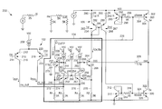
- FIG. 2 illustrates a simplified circuit diagram of the low-voltage op amp 100 in FIG. 1 .
- This simplified circuit diagram depicts a circuit 200 , which comprises the input stage 102 , intermediate stage 104 and output stage 106 shown in FIG. 1 .
- the intermediate stage 104 may also be referred to as a “differential current mode gain stage 104 .”
- Other embodiments of the circuit 200 may have additional stages.
- the input stage 102 in FIG. 2 comprises a current source 208 coupled to voltage source Vcc, a first transistor 210 and a second transistor 218 .
- the first and second transistors 210 , 218 comprise pnp bipolar junction transistors (BJTs).
- the first and second transistors 210 , 218 may be referred to as a pnp differential pair.
- the current source 208 comprises a 34-uA current source, which generates a current that may be split among the emitter terminals 212 , 220 of the transistors 210 , 218 , depending on the voltages of the base terminals 214 , 222 .
- the base terminal 214 of the first transistor 210 in the input stage 102 receives an inverting input (“inv”) of the op amp 100 .
- the base terminal 222 of the second transistor 218 in the input stage 102 receives a non-inverting input (“ni”) of the op amp 100 .
- the collector terminal 216 of the first transistor 210 provides a first input current I INP at an emitter terminal 252 of a transistor 245 of the differential current mode gain stage 104 .
- the collector terminal 224 of the second transistor 218 provides a second input current I INN at an emitter terminal 256 of a transistor 261 of the differential current mode gain stage 104 .
- the first and second transistors 210 , 218 of the input stage 102 drive the intermediate stage 104 with the input currents I INP and I INN .
- the differential current mode gain stage 104 in FIG. 2 comprises a first current source 228 , a second current source 230 , a third current source 232 , a first high impedance node A, a second high impedance mode B, a first transistor (Q 1 ) 237 , a second transistor (Q 2 ) 265 , a third transistor (Q 3 ) 245 , a fourth transistor (Q 4 ) 261 , a fifth transistor (Q 5 ) 243 , a sixth transistor (Q 6 ) 259 , a first resistor (R 1 ) 272 , a second resistor (R 2 ) 278 , a third resistor (R 3 ) 274 , a fourth resistor (R 4 ) 276 and a capacitor 270 .
- the differential current mode gain stage 104 may comprise other components in addition to or instead of the components shown in FIG. 2 .
- the differential current mode gain stage 104 may comprise less components than the components shown in
- the first, second and third current sources 228 , 230 , 232 in FIG. 2 are coupled to common supply voltage Vcc.
- the first and third current sources 228 , 232 each provide 23 uA of current, and the second current source 230 provides 4 uA of current, respectively.
- the first, second and third current sources 228 , 230 , 232 provide other amounts of current instead of 23 uA and 4 uA.
- the current sources 228 , 230 , 232 are constant.
- the current sources 228 , 230 , 232 are variable.
- the current sources 228 , 230 , 232 provide direct current.
- the transistors Q 1 -Q 6 in the differential current mode gain stage 104 are npn BJTs.
- the resistors R 1 , R 2 have a resistance of 5 kohms, and the resistors R 3 , R 4 have a resistance of 3 kohms.
- the capacitor 270 comprises a 2.5 picofarad capacitance. In other embodiments, the resistors R 1 -R 4 and the capacitor 270 may have other values.
- the first high impedance node A in FIG. 2 is coupled to the base terminal 238 of the transistor Q 1 and the collector terminal 248 of the transistor Q 3 .
- the second high impedance node B is coupled to the base terminal 266 of the transistor Q 2 and the collector terminal 254 of the transistor Q 4 .
- the current source 230 is coupled to the base terminals 244 , 250 , 260 of the transistors Q 3 , Q 4 , Q 5 , Q 6 and the collector terminals 242 , 258 of the transistors Q 5 , Q 6 .
- the transistors Q 5 , Q 6 in FIG. 2 are configured as diodes with the base terminals 244 , 260 coupled to the collector terminals 242 , 258 .
- the differential current mode gain stage 104 in FIG. 2 provides a high differential gain and a controlled common mode level at the first and second high impedance nodes A and B, as described below.
- the differential current mode gain stage 104 also keeps the transistors Q 3 , Q 4 out of saturation during normal operation.
- the output stage 106 in FIG. 2 comprises a first resistor 280 , a second resistor 290 , a first transistor 283 , a second transistor 287 , a third transistor 293 , a third resistor 298 , a first output transistor 300 , a capacitor 308 , a fourth transistor 310 , a fourth resistor 318 and a second output transistor 320 .
- the first, second and third transistors 283 , 287 , 293 comprise pnp transistors
- the fourth transistor 310 comprises a npn transistor.
- the first, third and fourth transistors 283 , 293 , 310 are configured as diodes with the base terminals 284 , 294 , 314 coupled to the collector terminals 234 , 296 , 312 .
- the first output transistor 300 comprises a pnp transistor
- the second output transistor 320 comprises a npn transistor.
- resistors 280 , 290 each comprise a 2-kohm resistor
- resistors 298 , 318 each comprise a 4-kohm resistor.
- the resistors 280 , 290 , 298 in FIG. 2 are coupled between the diode-configured, first transistor 283 and the first output transistor 300 and are configured to increase open loop gain.
- Bias is set up via a “common mode feedback loop” or a “common mode bias circuit,” which comprises the transistors Q 1 -Q 6 . If the voltage levels at nodes A and B are substantially equal, the diode-configured transistors Q 5 , Q 6 will conduct substantially the same amount of current.
- the voltage levels at nodes A and B will increase.
- the voltage levels of the emitter terminals 240 , 268 of transistors Q 1 , Q 2 will also increase.
- Higher voltage levels at the emitter terminals 240 , 268 of the transistors Q 1 , Q 2 (and nodes A and B) will “pull up” the transistors Q 5 , Q 6 because the emitter terminals 246 , 262 of the transistors Q 5 , Q 6 are coupled to the emitter terminals 240 , 268 of the transistors Q 1 , Q 2 , respectively.
- the pull up of the transistors Q 5 , Q 6 forces the voltage levels at the base terminals 244 , 250 , 260 of the transistors Q 3 -Q 6 to increase.
- the increased voltage level at the base terminals 244 , 250 , 260 of the transistors Q 3 -Q 6 causes the current entering the collector terminals 248 , 254 of the transistors Q 3 , Q 4 to increase.
- the increase in collector currents of the transistors Q 3 , Q 4 provides negative feedback.
- the feedback forces the transistors Q 3 , Q 4 to conduct all of the current provided by the current sources 228 , 232 (ignoring base currents of the transistors Q 1 , Q 2 ).
- the collector currents of the transistors Q 3 , Q 4 increase, the voltage levels of nodes A and B are pulled back down. Thus, the common mode feedback loop closes with a correct sign.
- the input stage 102 in FIG. 2 may force a common mode input current (e.g., I INP and I INN are in phase and have the same sign) (also called a “common mode signal”) into the emitter terminals 252 , 256 of the transistors Q 3 , Q 4 in the intermediate stage 104 .
- a common mode current can be observed at nodes A and B.
- the current sources 228 , 232 can be fixed, so the common mode current is forced into the base terminals 238 , 266 of the transistors Q 1 , Q 2 , which affects the voltages at nodes A and B.
- the common mode signal increases the voltage drop across the resistors R 3 and R 4 because the currents in the transistors Q 3 , Q 4 are fixed by the common mode feedback loop. Thus, substantially all of the input currents I INP and I INN flow into the resistors R 3 , R 4 .
- a differential input current is applied to two input nodes of the circuit, e.g., a voltage level at a first input node increases while a voltage level at a second input node decreases, the common mode level of the circuit does not change significantly. If low collector-emitter voltages (Vces) are required in the common mode feedback circuit, then one or more of the transistors in the circuit may saturate.
- Vces collector-emitter voltages
- low collector-emitter voltages are desired without causing one or more transistors, e.g., the transistors Q 3 , Q 4 , to saturate.
- the input stage 102 in FIG. 2 may force a small differential input current (e.g., I INP and I INN are out of phase and/or one is greater in amplitude than the other) into the emitter terminals 252 , 256 of the transistors Q 3 , Q 4 .
- the current sources 228 , 232 can be fixed, so the differential current is forced into the base terminals 238 , 266 of the transistors Q 1 , Q 2 , which affects the voltages at nodes A and B.
- the voltage level at node A may increase slightly, while the voltage level at node B may decrease slightly.
- the different voltage levels at nodes A and B cause the emitter terminals 240 , 268 of the transistors Q 1 and Q 2 , and hence the emitter terminals 246 , 262 of the transistors Q 5 and Q 6 , to have different voltage levels.
- the higher voltage level at the emitter terminal 246 of transistor Q 5 causes the current from the current source 230 to shift from an equal split between the transistors Q 5 , Q 6 to mostly flowing into the transistor Q 6 .
- the absolute value of the increased voltage level at node A is equal to the absolute value of the decreased voltage level at node B.
- This balanced differential voltage change does not change the voltage level at the base terminals 250 of the transistors Q 3 , Q 4 , in contrast to the common mode example described above.
- the common mode feedback loop does not react, and all of the differential input current flows through the transistors Q 3 , Q 4 into the base terminals of the transistors Q 1 and Q 2 , which results in a small signal differential gain of beta in transistors Q 1 and Q 2 .
- Beta is the ratio of a total current in a collector terminal to a total current in a base terminal for a particular transistor (beta may also be called the common-emitter current gain).
- An additional differential signal (e.g., increasing the difference between the input currents I INP and I INN by increasing I INP and/or decreasing I INN ) may cause one of the diode-configured transistors Q 5 or Q 6 to shut off, which changes the voltage level behavior at nodes A and B.
- I INP and I INN e.g., increasing the difference between the input currents I INP and I INN by increasing I INP and/or decreasing I INN
- the voltage level at node A increases, while the voltage level at node B decreases, which forces current from the second current source 230 to shift from an equal split between the transistors Q 5 , Q 6 to mostly flowing into the transistor Q 6 .
- the behavior of the intermediate stage 104 changes.
- Node B is now held at a fixed voltage with respect to the base 250 of the transistor Q 4 by the voltage loop through the transistors Q 6 and Q 2 base-emitter voltages.
- the fixed voltage at node B with respect to the base voltage of the transistor Q 4 keeps transistor Q 4 from saturating.
- the transistor Q 6 now controls the base voltage of the transistors Q 3 and Q 4 without the transistor Q 5 to balance the base voltage.
- Node A is not constrained by common mode feedback because the transistor Q 5 is off. Thus, the voltage level at node A may continue to increase. The increasing voltage level at node A with respect to the base voltage of the transistor Q 3 keeps transistor Q 3 out of saturation. The large signal differential gain shifts to the transistor Q 3 . Thus, the differential current mode gain stage 104 shifts from separate common mode and differential mode actions to a merged action, where large differential mode signals cause a shift in the common mode level. The differential current mode gain stage 104 is stable in operation.
- the transistors Q 1 , Q 2 convert the differential current signals to first and second output currents I OUTP and I OUTN , respectively, which enter the emitter terminals 236 , 264 of the transistors Q 1 , Q 2 .
- the intermediate stage 104 drives the output stage 106 with the output currents I OUTP and I OUTN .
- the output currents I OUTP and I OUTN in FIG. 2 are not current-limited.
- the output current(s) I OUTP and/or I OUTN of the circuit 200 in FIG. 2 continually increases until a voltage drop across the resistors R 1 and R 2 causes a transistor in the circuit 200 to saturate from being too close to the supply voltage. This is a significant improvement over an op amp circuit (not shown) with a fixed maximum current, which is usually fixed by a bias current of the input stage.
- the output current of one embodiment of the intermediate stage 104 is limited only by the available supply voltage Vcc and the beta value of the transistors Q 1 -Q 6 .
- the op amp 100 in FIG. 1 further comprises a short-circuit protection circuit 107 .
- the output current capability of the circuit 200 is greater than a short circuit, current limit control setpoint for supply voltages between about 2.7 to about 5 volts (i.e., the output current capability is limited by the short circuit current limit circuitry). Below about 2.7 volts, the output current capability drops in proportion to the supply voltage.
- feedback capacitor 308 in the output stage 106 and capacitor 270 in the intermediate stage 104 are sufficient to stabilize the intermediate stage 104 and the circuit 200 .
- the diode current may shift from an equal split between the transistors Q 5 , Q 6 to mostly flowing into the transistor Q 6 .
- the output (at best) may peak undesirably because the feedback capacitor 308 is no longer providing as much compensation compared to when no output current is drawn.
- the collector current of the transistor Q 2 may drop to below 10 uA. This drop makes the transistor Q 2 much less effective at driving the base 260 of the transistor Q 6 and the resistor R 2 because the transconductance (gm) of the transistor Q 2 has dropped to a low value. Instead of modulating the base voltage of the transistor Q 6 , most of the modulation occurs in the gm of the transistor Q 2 .
- the oscillation is caused by the feedback compensation capacitor 308 connected to node B via the transistors Q 2 , Q 6 . When the gm of the transistor Q 2 becomes sufficiently low, the compensation is disabled, which causes peaking.
- the bias current source 230 is 4 uA, as shown in FIG. 2 .
- the diode bias current is significantly smaller than the current in the transistor Q 2 , even when the circuit 200 is sourcing near its maximum current.
- the current supply 230 should be smaller than current supplies 228 and 232 .
- the magnitude 4 uA is an example in one embodiment.
- FIG. 3 illustrates one embodiment of a bias circuit 108 for the low-voltage op amp 100 in FIG. 1 .
- the bias circuit 108 provides the op amp 100 in FIG. 1 with a low supply voltage Vcc.
- the bias circuit 108 comprises a first transistor 330 , a second transistor 336 , a third transistor 340 , a fourth transistor 344 , a fifth transistor 350 , a first transistor set 352 (which, for clarity, is represented by a single transistor), a sixth transistor 358 , a seventh transistor 356 , a second transistor set 360 (which, for clarity, is represented by a single transistor), a capacitor 346 , a first resistor 332 , a second resistor 334 , a third resistor 338 , a fourth resistor 342 , a fifth resistor 348 , a sixth resistor 354 and a pbias output terminal 362 .
- the pbias output terminal 362 can be coupled to base terminals of the transistors above the input stage 102 and the intermediate stage 104 in FIG. 1 .
- pbias output terminal 362 may be coupled to low voltage op amp 100 at the “Vcc” terminal.
- the transistors 330 , 336 , 340 , 350 , 358 in FIG. 3 comprise pnp transistors. In one embodiment, the transistors 344 , 356 comprise npn transistors. In one embodiment, the transistor set 352 comprises two npn transistors coupled in parallel. In one embodiment, the transistor set 360 comprises six npn transistors coupled in parallel.
- the resistor 332 comprises a 6-kohm resistor
- the resistor 334 comprises an 84-kohm resistor
- the resistor 338 comprises a 10.5-kohm resistor
- the resistor 342 comprises a 7.5-kohm resistor
- the resistor 348 comprises a 36-kohm resistor
- the resistor 354 comprises an 80-kohm resistor.
- the capacitor 346 comprises a 1-picofarad capacitor.
- Portions of the bias circuit 108 in FIG. 3 operate as a peaking current source circuit, which is exemplified by circuit 400 shown in FIG. 4 .
- FIG. 4 illustrates one embodiment of a peaking current source circuit 400 , which exemplifies the operation of portions of the bias circuit 108 in FIG. 3 .
- the peaking current source circuit 400 comprises an input current source 402 , a resistor 404 , a first transistor 406 and a second transistor 408 .
- the resistor 404 is a 1-kohm resistor
- the transistors 406 , 408 are npn transistors.
- the peaking current source circuit 400 in FIG. 4 has an output current I OUT that is about equal to an input current I in when the voltage drop across the resistor 404 is negligible. As the input current I in increases, the voltage drop across the resistor 404 increases. At high input currents, the output current I out actually decreases. Thus, the current source circuit 400 may be called a “peaking current source.”
- the bias circuit 108 comprises two cascaded peaking current source circuits and other components.
- the first cascaded peaking current source circuit comprises the resistor 342 , transistor 344 and the transistor set 352 .
- the second cascaded peaking current source circuit comprises the transistors 330 , 336 and the resistor 332 .
- the two cascaded peaking current source circuits reject a variation in reference current, which flows in resistor 334 , caused by a variation in supply voltage Vcc.
- the bias circuit 108 also comprises a linear current term added by the transistor and the resistor 338 to further dampen variation of circuit bias with respect to Vcc.
- the bias circuit 108 works well across various process and temperature conditions.
- FIG. 5 illustrates one embodiment of a differential current mode gain stage within the low-voltage op amp 100 of FIG. 1 .
- FIG. 6 illustrates an example of an AC differential gain and a common mode gain of one embodiment of the intermediate stage 104 in FIG. 1 with respect to a frequency of an AC input signal.
- Differential gain is plotted by a first line 600
- common mode gain is plotted by a second line 602 .
- gain is defined as I OUT /I IN .
- the differential gain 600 is greater than the common mode gain 602 between a frequency range of about 1 Hz to about 100 MHz, as shown in Figure.
- the differential gain 600 between about 1 Hz and about 1 MHz, when I INP and I INN are 180 degrees out of phase is about 34.895 dB.
- the common mode gain 602 between about 1 Hz to about 100 MHz, when I INP and I INN are in phase, is about ⁇ 4.6334 dB.
- the relatively low common mode gain allows easy control of the common mode bias point.
- FIG. 7 is a table of values associated with one embodiment of the op amp 100 in FIG. 1 .
- Av+1 represents a closed-loop op amp voltage gain (of the op amp 100 ) of +1.
- Av+2 represents a closed-loop op amp gain of +2.
- a plurality of exemplifying supply voltages (1.2V, 2.7V, 5V and +/ ⁇ 2.5V) are applied to the op amp 100 of FIG. 1 .
- Icc represents a supply current of the op amp 100 .
- Vos represents an input offset voltage error of the op amp 100 .
- Ib represents an input bias current at the base terminals 214 , 222 of the transistors 210 , 218 of the input stage 102 , which receive the inv and ni signals.
- Ao represents an open loop gain of the op amp 100 .
- PSRR represents a power supply rejection ratio of the op amp 100 .
Landscapes
- Engineering & Computer Science (AREA)
- Power Engineering (AREA)
- Amplifiers (AREA)
Abstract
Description
Claims (17)
Priority Applications (2)
| Application Number | Priority Date | Filing Date | Title |
|---|---|---|---|
| US09/863,574 US6469578B1 (en) | 2001-05-23 | 2001-05-23 | Differential current mode gain stage and methods of using the same |
| US10/155,520 US20020175755A1 (en) | 2001-05-23 | 2002-05-24 | Differential current mode gain stage and methods of using the same |
Applications Claiming Priority (1)
| Application Number | Priority Date | Filing Date | Title |
|---|---|---|---|
| US09/863,574 US6469578B1 (en) | 2001-05-23 | 2001-05-23 | Differential current mode gain stage and methods of using the same |
Related Child Applications (1)
| Application Number | Title | Priority Date | Filing Date |
|---|---|---|---|
| US10/155,520 Continuation US20020175755A1 (en) | 2001-05-23 | 2002-05-24 | Differential current mode gain stage and methods of using the same |
Publications (1)
| Publication Number | Publication Date |
|---|---|
| US6469578B1 true US6469578B1 (en) | 2002-10-22 |
Family
ID=25341321
Family Applications (2)
| Application Number | Title | Priority Date | Filing Date |
|---|---|---|---|
| US09/863,574 Expired - Lifetime US6469578B1 (en) | 2001-05-23 | 2001-05-23 | Differential current mode gain stage and methods of using the same |
| US10/155,520 Abandoned US20020175755A1 (en) | 2001-05-23 | 2002-05-24 | Differential current mode gain stage and methods of using the same |
Family Applications After (1)
| Application Number | Title | Priority Date | Filing Date |
|---|---|---|---|
| US10/155,520 Abandoned US20020175755A1 (en) | 2001-05-23 | 2002-05-24 | Differential current mode gain stage and methods of using the same |
Country Status (1)
| Country | Link |
|---|---|
| US (2) | US6469578B1 (en) |
Cited By (4)
| Publication number | Priority date | Publication date | Assignee | Title |
|---|---|---|---|---|
| US6636111B1 (en) * | 2002-07-26 | 2003-10-21 | Linear Technology Corporation | Bootstrap circuit to cancel input bias currents of a differential amplifier over most of common-mode input voltage range |
| US20050189992A1 (en) * | 2004-02-27 | 2005-09-01 | Analog Devices, Inc. | Bipolar differential input stage with input bias current cancellation circuit |
| US7215200B1 (en) * | 2005-04-28 | 2007-05-08 | Linear Technology Corporation | High-linearity differential amplifier with flexible common-mode range |
| US9431978B2 (en) | 2013-07-31 | 2016-08-30 | Fairchild Semiconductor Corporation | Common-mode feedback differential amplifier |
Families Citing this family (1)
| Publication number | Priority date | Publication date | Assignee | Title |
|---|---|---|---|---|
| CN108494377B (en) * | 2018-04-11 | 2022-02-01 | 锐芯微电子股份有限公司 | Operational amplifier circuit |
Citations (2)
| Publication number | Priority date | Publication date | Assignee | Title |
|---|---|---|---|---|
| US5706236A (en) * | 1992-11-30 | 1998-01-06 | Fujitsu Limited | Semiconductor memory device |
| US6184750B1 (en) * | 1999-05-27 | 2001-02-06 | Gain Technology, Inc. | Control circuit driven by a differential input voltage and method for controlling same |
-
2001
- 2001-05-23 US US09/863,574 patent/US6469578B1/en not_active Expired - Lifetime
-
2002
- 2002-05-24 US US10/155,520 patent/US20020175755A1/en not_active Abandoned
Patent Citations (2)
| Publication number | Priority date | Publication date | Assignee | Title |
|---|---|---|---|---|
| US5706236A (en) * | 1992-11-30 | 1998-01-06 | Fujitsu Limited | Semiconductor memory device |
| US6184750B1 (en) * | 1999-05-27 | 2001-02-06 | Gain Technology, Inc. | Control circuit driven by a differential input voltage and method for controlling same |
Non-Patent Citations (1)
| Title |
|---|
| "A Wide-Band Operational Amplifier With a New Output Stage and a Simple Frequency Compensation," Rudy J. van De Plassche; IEEE Journal of Solid-State Circuits, vol. SC-6, No. 6, Dec. 1971, pp. 347-352. |
Cited By (5)
| Publication number | Priority date | Publication date | Assignee | Title |
|---|---|---|---|---|
| US6636111B1 (en) * | 2002-07-26 | 2003-10-21 | Linear Technology Corporation | Bootstrap circuit to cancel input bias currents of a differential amplifier over most of common-mode input voltage range |
| US20050189992A1 (en) * | 2004-02-27 | 2005-09-01 | Analog Devices, Inc. | Bipolar differential input stage with input bias current cancellation circuit |
| US6965267B2 (en) * | 2004-02-27 | 2005-11-15 | Analog Devices, Inc. | Bipolar differential input stage with input bias current cancellation circuit |
| US7215200B1 (en) * | 2005-04-28 | 2007-05-08 | Linear Technology Corporation | High-linearity differential amplifier with flexible common-mode range |
| US9431978B2 (en) | 2013-07-31 | 2016-08-30 | Fairchild Semiconductor Corporation | Common-mode feedback differential amplifier |
Also Published As
| Publication number | Publication date |
|---|---|
| US20020175755A1 (en) | 2002-11-28 |
Similar Documents
| Publication | Publication Date | Title |
|---|---|---|
| US6429700B1 (en) | Driver circuit with output common mode voltage control | |
| US7532072B1 (en) | Method to control the output common mode in a differential OPAMP with rail-to-rail input stage | |
| US8502603B2 (en) | Output common mode voltage stabilizer over large common mode input range in a high speed differential amplifier | |
| JP2008543178A (en) | High speed settling, low noise, low offset operational amplifier and method | |
| JPH0360209A (en) | Amplifier circuit and semiconductor integrated circuit including the same | |
| US5774019A (en) | Low distortion differential amplifier circuit | |
| US8866554B2 (en) | Translinear slew boost circuit for operational amplifier | |
| US7728669B2 (en) | Output stage circuit and operational amplifier thereof | |
| US6788143B1 (en) | Cascode stage for an operational amplifier | |
| US6114912A (en) | Integrated amplifier having a voltage-controlled current source | |
| US6469578B1 (en) | Differential current mode gain stage and methods of using the same | |
| KR987001154A (en) | amplifier | |
| JPH08237054A (en) | Gain variable circuit | |
| US7109802B2 (en) | Bipolar differential to single ended transfer circuit with gain boost | |
| US6657496B2 (en) | Amplifier circuit with regenerative biasing | |
| US6781462B2 (en) | Power amplifier | |
| US6809589B2 (en) | Low voltage large swing/high linearity analog buffer with servo amplifier and feedback loop | |
| JP2012028859A (en) | Variable gain differential amplifier circuit | |
| US6879608B1 (en) | High compliance laser driver | |
| US7170337B2 (en) | Low voltage wide ratio current mirror | |
| US6175226B1 (en) | Differential amplifier with common-mode regulating circuit | |
| US5440273A (en) | Rail-to-rail gain stage of an amplifier | |
| US6366170B1 (en) | PNP high-current, high-swing output stage and method | |
| US6420931B1 (en) | High swing output circuit having differential to single-ended conversion and method | |
| US7019590B1 (en) | Self-stabilizing differential load circuit with well controlled impedance |
Legal Events
| Date | Code | Title | Description |
|---|---|---|---|
| AS | Assignment |
Owner name: FAIRCHILD SEMICONDUCTOR CORPORATION, A DELAWARE CO Free format text: ASSIGNMENT OF ASSIGNORS INTEREST;ASSIGNOR:SMITH, STEVEN OBED;REEL/FRAME:011844/0710 Effective date: 20010521 |
|
| STCF | Information on status: patent grant |
Free format text: PATENTED CASE |
|
| FPAY | Fee payment |
Year of fee payment: 4 |
|
| FPAY | Fee payment |
Year of fee payment: 8 |
|
| FPAY | Fee payment |
Year of fee payment: 12 |
|
| AS | Assignment |
Owner name: FAIRCHILD SEMICONDUCTOR CORPORATION, MAINE Free format text: CORRECTIVE ASSIGNMENT TO CORRECT THE NAME OF THE RECEIVING PARTY PREVIOUSLY RECORDED ON REEL 011844 FRAME 0710. ASSIGNOR(S) HEREBY CONFIRMS THE ASSIGNMENT;ASSIGNOR:SMITH, STEVEN OBED;REEL/FRAME:039490/0788 Effective date: 20010521 |
|
| AS | Assignment |
Owner name: DEUTSCHE BANK AG NEW YORK BRANCH, AS COLLATERAL AGENT, NEW YORK Free format text: PATENT SECURITY AGREEMENT;ASSIGNOR:FAIRCHILD SEMICONDUCTOR CORPORATION;REEL/FRAME:040075/0644 Effective date: 20160916 Owner name: DEUTSCHE BANK AG NEW YORK BRANCH, AS COLLATERAL AG Free format text: PATENT SECURITY AGREEMENT;ASSIGNOR:FAIRCHILD SEMICONDUCTOR CORPORATION;REEL/FRAME:040075/0644 Effective date: 20160916 |
|
| AS | Assignment |
Owner name: SEMICONDUCTOR COMPONENTS INDUSTRIES, LLC, ARIZONA Free format text: ASSIGNMENT OF ASSIGNORS INTEREST;ASSIGNOR:FAIRCHILD SEMICONDUCTOR CORPORATION;REEL/FRAME:057694/0374 Effective date: 20210722 |
|
| AS | Assignment |
Owner name: FAIRCHILD SEMICONDUCTOR CORPORATION, ARIZONA Free format text: RELEASE BY SECURED PARTY;ASSIGNOR:DEUTSCHE BANK AG NEW YORK BRANCH;REEL/FRAME:057969/0206 Effective date: 20211027 Owner name: FAIRCHILD SEMICONDUCTOR CORPORATION, ARIZONA Free format text: RELEASE OF SECURITY INTEREST;ASSIGNOR:DEUTSCHE BANK AG NEW YORK BRANCH;REEL/FRAME:057969/0206 Effective date: 20211027 |
|
| AS | Assignment |
Owner name: DEUTSCHE BANK AG NEW YORK BRANCH, AS COLLATERAL AGENT, NEW YORK Free format text: SECURITY INTEREST;ASSIGNOR:SEMICONDUCTOR COMPONENTS INDUSTRIES, LLC;REEL/FRAME:058871/0799 Effective date: 20211028 |
|
| AS | Assignment |
Owner name: FAIRCHILD SEMICONDUCTOR CORPORATION, ARIZONA Free format text: RELEASE OF SECURITY INTEREST IN PATENTS RECORDED AT REEL 040075, FRAME 0644;ASSIGNOR:DEUTSCHE BANK AG NEW YORK BRANCH, AS COLLATERAL AGENT;REEL/FRAME:064070/0536 Effective date: 20230622 Owner name: SEMICONDUCTOR COMPONENTS INDUSTRIES, LLC, ARIZONA Free format text: RELEASE OF SECURITY INTEREST IN PATENTS RECORDED AT REEL 040075, FRAME 0644;ASSIGNOR:DEUTSCHE BANK AG NEW YORK BRANCH, AS COLLATERAL AGENT;REEL/FRAME:064070/0536 Effective date: 20230622 |
|
| AS | Assignment |
Owner name: FAIRCHILD SEMICONDUCTOR CORPORATION, ARIZONA Free format text: RELEASE OF SECURITY INTEREST IN PATENTS RECORDED AT REEL 058871, FRAME 0799;ASSIGNOR:DEUTSCHE BANK AG NEW YORK BRANCH, AS COLLATERAL AGENT;REEL/FRAME:065653/0001 Effective date: 20230622 Owner name: SEMICONDUCTOR COMPONENTS INDUSTRIES, LLC, ARIZONA Free format text: RELEASE OF SECURITY INTEREST IN PATENTS RECORDED AT REEL 058871, FRAME 0799;ASSIGNOR:DEUTSCHE BANK AG NEW YORK BRANCH, AS COLLATERAL AGENT;REEL/FRAME:065653/0001 Effective date: 20230622 |