US6423969B1 - Dual infrared band objective lens - Google Patents

Dual infrared band objective lens Download PDF

Info

Publication number
US6423969B1
US6423969B1 US08/310,108 US31010894A US6423969B1 US 6423969 B1 US6423969 B1 US 6423969B1 US 31010894 A US31010894 A US 31010894A US 6423969 B1 US6423969 B1 US 6423969B1
Authority
US
United States
Prior art keywords
lens
air
matl
optical imaging
imaging system
Prior art date
Legal status (The legal status is an assumption and is not a legal conclusion. Google has not performed a legal analysis and makes no representation as to the accuracy of the status listed.)
Expired - Fee Related
Application number
US08/310,108
Inventor
Max Amon
Current Assignee (The listed assignees may be inaccurate. Google has not performed a legal analysis and makes no representation or warranty as to the accuracy of the list.)
Lockheed Martin Corp
Original Assignee
Lockheed Martin Corp
Priority date (The priority date is an assumption and is not a legal conclusion. Google has not performed a legal analysis and makes no representation as to the accuracy of the date listed.)
Filing date
Publication date
Application filed by Lockheed Martin Corp filed Critical Lockheed Martin Corp
Priority to US08/310,108 priority Critical patent/US6423969B1/en
Assigned to MARTIN MARIETTA CORPORATION reassignment MARTIN MARIETTA CORPORATION ASSIGNMENT OF ASSIGNORS INTEREST (SEE DOCUMENT FOR DETAILS). Assignors: AMON, MAX
Priority to US09/116,809 priority patent/US7408159B1/en
Assigned to LOCKHEED MARTIN CORPORATION reassignment LOCKHEED MARTIN CORPORATION ASSIGNMENT OF ASSIGNORS INTEREST (SEE DOCUMENT FOR DETAILS). Assignors: MARTIN MARIETTA CORPORATION
Application granted granted Critical
Publication of US6423969B1 publication Critical patent/US6423969B1/en
Anticipated expiration legal-status Critical
Expired - Fee Related legal-status Critical Current

Links

Images

Classifications

    • GPHYSICS
    • G02OPTICS
    • G02BOPTICAL ELEMENTS, SYSTEMS OR APPARATUS
    • G02B13/00Optical objectives specially designed for the purposes specified below
    • G02B13/14Optical objectives specially designed for the purposes specified below for use with infrared or ultraviolet radiation
    • G02B13/146Optical objectives specially designed for the purposes specified below for use with infrared or ultraviolet radiation with corrections for use in multiple wavelength bands, such as infrared and visible light, e.g. FLIR systems

Definitions

  • the present invention relates to an objective lens system and, in particular, a Petzval objective, capable of simultaneous dual band imagery in both the 3-5 and 8-12 micrometer spectral ranges, for use with a dual spectral band detector, such as a quantum well detector.
  • a dual spectral band detector such as a quantum well detector.
  • Recent advancements in quantum well detector technologies permit the simultaneous processing and display of dual infrared band imagery with a single detector at a single focal plane. There are advantages of imaging each spectral band and the possibility of focusing both bands simultaneously may yield greater information for surveillance and/or target discrimination by imaging devices.
  • Imaging devices, search and track sensors such as forward looking infrared systems, and other types of optical devices which operate in the 3-12 micrometer spectral region use either reflective or refractive objective lens systems.
  • An advantage of reflective optics is that they operate within a wide spectral band.
  • reflective optics systems have several undesirable features, such as, for example, a more limited field of view and a large physical size.
  • central obstructions in reflective optics limit the modulation transfer function (MTF), or sine wave response.
  • MTF modulation transfer function
  • refractive lens systems have been designed for limited ranges, e.g., either the 3-5 or the 8-12 micrometer bands. This is because the refractive indices of the component lens materials vary significantly between the two spectral bands. For example, germanium behaves like a crown (a low dispersion material) in the 8-12 micrometer wavelengths and like a flint (a high dispersion material) in the 3-5 micrometer region. Systems designed to operate in one band exhibit intolerable chromatic aberrations in the other band. The design for either long wave (8-12 micrometers) or short wave (3-5 micrometers) lenses are commonplace, but the need for simultaneous dual band operation is a relatively new requirement.
  • optical materials that can transmit wavelengths in the spectral range of interest for this application is limited, and many infrared lens materials are soft or water soluble, which make them unsuitable for tactical systems.
  • the present invention overcomes the problems of the prior art by providing a combination of lens materials that yield excellent broad band color correction in the 3-12 micron spectral range; that are durable, easily produced and highly reliable; and therefore that are suitable for tactical infrared imaging systems.
  • the present invention is an optical lens system made up of at least one lens triplet of a negative zinc sulfide lens, a positive zinc selenide lens, and a negative gallium arsenide lens, each of the lenses being positioned along a chief ray for simultaneous dual band imagery in both the 3-5 and 8-12 micrometer spectral bands.
  • the lens system can include two widely spaced, net positive triplets, forming a Petzval-type lens.
  • a quantum well detector may be placed at the focal plane for dual band image detection.
  • FIG. 1 illustrates a YZ profile of a wide band Petzval objective lens employing two widely spaced triplets in accordance with the present invention
  • FIGS. 2 a - 2 c are spot diagrams illustrating the performance achieved in the spectral band of 3-5 micrometers.
  • FIGS. 3 a - 3 c are spot diagrams illustrating the performance achieved in the spectral band of 8-12 micrometers.
  • the index of refraction of optical materials varies with wavelength.
  • the refractive index is generally higher at shorter wavelengths so that light converges faster (the focal length is shorter) than at longer wavelengths.
  • This spread in the focal position over a spectral range is the primary chromatic aberration called axial color. It is relatively easy to correct the axial color aberration in either the 3-5 or the 8-12 micrometer spectral range by simply combining low and high dispersion elements and dividing the magnification power of the lens system among positive and negative lens elements. Color correction of both bands is much more difficult.
  • the present inventor has discovered a unique combination of lens powers, including an aspheric surface, and materials that yield color correction for both spectral bands simultaneously.
  • the type of lens and the materials are, in order of their appearance along a chief ray of a focal optical lens system, as follows:
  • Effective Focal Length 7.5′′ f/# 2.0 Field of View 4.0 ⁇ 4.0 degrees Pixel Size 0.002′′ Format Size 0.5 ⁇ 0.5 Spectral Range 3 to 5 ⁇ m and 8 to 12 ⁇ m Cold Shield Efficiency 100%
  • Speed refers to the light gathering power of the lens.
  • this property of the lens system is indicated by the f/number.
  • the exposure time required for a given photograph is proportional to the square of the f/number and will be shorter when a lens with a low f/number is used; thus, a lens having a higher speed reduces light gathering time.
  • Petzval-type lens Two widely spaced triplets in the form of a Petzval-type lens provide an optimum speed and field of view for the above-listed lens characteristics.
  • a classic Petzval lens involves two spaced doublets, but the term is used here by analogy because each triplet is a net positive lens group.
  • the six element combination with two aspheric surfaces can be optimized on the ACCOSV optical design program.
  • AD, AE, AF and AG represent 4th, 6th, 8th and 10th order deformation coefficients, respectively and the asterisk * signifies where the aperture stop/cold shield is located.
  • These refractive indices correspond to the 8-12 micrometer range and are different for the 3-5 micrometer range when generating the spot diagrams of FIGS. 2 a - 2 c .
  • lens characteristics can be used within the scope of the present invention.
  • the above data is exemplary and reflects an optimum lens data for a particular quantum well detector chip.
  • a first lens 10 , 13 is negative
  • a second lens 11 , 14 is positive
  • a third lens 12 , 15 is negative as taken along the chief ray.
  • Surfaces 10 B and 13 B of the ZNS lens are selected for receiving aspheric surfaces.
  • ZnS is a diamond turnable lens material which greatly eases manufacturing requirements.
  • the CleartranTM method provides a better, more homogenous material (C_ZnS) which is clearer in the 3-5 micrometer range than produced by some other methods.
  • a quantum well detector 19 can be placed at the image plane 18 .
  • a cryogenic vessel or Dewar houses the quantum well detector 19 to maintain the detector 19 at a temperature of approximately 77° Kelvin in order to increase detector sensitivity.
  • the cold shield 20 of the Dewar is shown.
  • optimum performance is achieved by cold shielding the detector array. This is done by introducing a cold diaphragm, or cold shield 20 , with an aperture stop 17 in front of the detector array so that the viewing angle of the detector to the warm background is limited as nearly as possible to only that required for transmission of radiation from the scene. Since the amount of radiation reaching the detector from the cold shield 20 is negligible compared to the amount reaching the detector from the warm background of the field of view, induced noise in the detector is minimized.
  • the cold shield 20 is typically placed within the Dewar. Also included in the optical system may be a Dewar window 16 .
  • FIGS. 2 a - 2 c and 3 a - 3 c The performance achieved in each spectral band is shown by the spot diagrams in FIGS. 2 a - 2 c and 3 a - 3 c .
  • Rays representative of three wavelengths in each of the 3 to 5 and 8 to 12 spectral bands from an on-axis and two off-axis field points are distributed through the full aperture and are traced through the system, producing FIGS. 2 c , 2 a and 2 b , respectively.
  • the FOB-Y is 1.0000 and the FOB-X is 0.0000
  • FIG. 2 b the FOB-Y is 0.7000 and the FOB-X is 0.0000; in FIG.
  • the FOB-Y is 0.0000 and the FOB-X is 0.0000; in FIG. 3 a , the FOB-Y is 1.0000 and the FOB-X is 0.0000; in FIG. 3 b , the FOB-Y is 0.7071 and the FOB-X is 0.0000; and in FIG. 3 c , the FOB-Y is 0.0000 and the FOB-X is 0.0000, wherein FOB stands for fractional object height.
  • FOB refers to the object point (or field angle when the object is at infinity) from which rays are traced.
  • the square in phantom is the pixel size of a typical quantum well detector, e.g., 50.8 ⁇ 50.8 micrometers (0.002 inches).
  • a typical quantum well detector e.g., 50.8 ⁇ 50.8 micrometers (0.002 inches).
  • all spot diagram origins are on the chief ray. Since virtually all of the ray intercepts are contained within the pixel, the image resolution will be limited by such a detector.
  • a quantum well detector's capability could go under-utilized without an optical system such as disclosed herein that can simultaneously deliver the image quality required over both the 3 to 5 ⁇ m and 8 to 5 ⁇ m spectral bands.
  • the lens system in accordance with the present invention yields excellent broadband color correction by a combination of infrared lens material suitable for tactical applications.
  • a beam splitter may be introduced into the lens system to split an image into the 3-5 ⁇ m range and the 8-12 ⁇ m range, whereupon the lens powers may vary and color correction requirements loosened because of the using more than one focal plane.
  • the lens system can be useful with detectors capable of imaging either the 3 to 5 ⁇ m or 8 to 12 ⁇ m spectral bands, and an imaging system can be envisioned wherein high and low spectral band detectors can be selectively placed at the focal plane(s), by use of a beam splitter or employing a detector change-over mechanism. Naturally, optimum performance is achieved when employing a single detector capable of detecting both the 3 to 5 ⁇ m and 8 to spectral bands.
  • the foregoing description is offered as illustrative and not limitative. Other variations and equivalents thereof are intended to be encompassed by the invention, which is defined by the claims appended hereto.

Abstract

An infrared refractive lens triplet having color correction properties for radiation within the 3 to 12 micrometer spectral band for use with a quantum well detector for simultaneous dual band imagery. In certain embodiments of the invention, two widely spaced triplets form a Petzval-type objective lens. Each lens triplet is made up of a negative zinc sulfide lens, a positive zinc selenide lens, and a negative gallium arsenide lens coaxially positioned along a chief ray of the lens system.

Description

BACKGROUND
1) Field of the Invention
The present invention relates to an objective lens system and, in particular, a Petzval objective, capable of simultaneous dual band imagery in both the 3-5 and 8-12 micrometer spectral ranges, for use with a dual spectral band detector, such as a quantum well detector.
2) Discussion of Related Art
Recent advancements in quantum well detector technologies permit the simultaneous processing and display of dual infrared band imagery with a single detector at a single focal plane. There are advantages of imaging each spectral band and the possibility of focusing both bands simultaneously may yield greater information for surveillance and/or target discrimination by imaging devices.
Imaging devices, search and track sensors such as forward looking infrared systems, and other types of optical devices which operate in the 3-12 micrometer spectral region use either reflective or refractive objective lens systems. An advantage of reflective optics is that they operate within a wide spectral band. However, reflective optics systems have several undesirable features, such as, for example, a more limited field of view and a large physical size. In addition, central obstructions in reflective optics limit the modulation transfer function (MTF), or sine wave response.
Additionally, efficient cold shielding is important with any cooled detector array. Reflective optics are not appropriate for wide field of view applications, particularly when efficient cold shielding is necessary.
In the past, refractive lens systems have been designed for limited ranges, e.g., either the 3-5 or the 8-12 micrometer bands. This is because the refractive indices of the component lens materials vary significantly between the two spectral bands. For example, germanium behaves like a crown (a low dispersion material) in the 8-12 micrometer wavelengths and like a flint (a high dispersion material) in the 3-5 micrometer region. Systems designed to operate in one band exhibit intolerable chromatic aberrations in the other band. The design for either long wave (8-12 micrometers) or short wave (3-5 micrometers) lenses are commonplace, but the need for simultaneous dual band operation is a relatively new requirement.
The number of optical materials that can transmit wavelengths in the spectral range of interest for this application is limited, and many infrared lens materials are soft or water soluble, which make them unsuitable for tactical systems.
Several studies have been carried out to isolate optical material combinations that yield refractive lens designs that are color corrected over the entire 3-12 micron spectral region. The following publications describe such studies: Thomas H. Jamieson, “Ultrawide Waveband Optics”, Optical Engineering, Vol. 23, No. 2, April 1984, pages 111-116; M. O. Lidwell, “Achromatism of Lenses for Thermal IR”, Proceedings SPIE, Vol. 518, 1984, pages 73-80; and, M. Roberts and P. Rogers, “Wide Waveband Infrared Optics”, Proceedings SPIE, Vol. 1013, 1988, pages 84-91.
These publications describe optical design studies that employ many different infrared lens material combinations. The solutions described in these studies yield excellent color correction over the spectral range of 3-12 microns, but the material combinations are poor choices from the standpoint of durability, manufacturability and reliability.
SUMMARY
The present invention overcomes the problems of the prior art by providing a combination of lens materials that yield excellent broad band color correction in the 3-12 micron spectral range; that are durable, easily produced and highly reliable; and therefore that are suitable for tactical infrared imaging systems.
Specifically, the present invention is an optical lens system made up of at least one lens triplet of a negative zinc sulfide lens, a positive zinc selenide lens, and a negative gallium arsenide lens, each of the lenses being positioned along a chief ray for simultaneous dual band imagery in both the 3-5 and 8-12 micrometer spectral bands. Alternatively, the lens system can include two widely spaced, net positive triplets, forming a Petzval-type lens. A quantum well detector may be placed at the focal plane for dual band image detection.
BRIEF DESCRIPTION OF THE DRAWINGS
The invention may be best understood by reference to the following detailed description when read in conjunction with the following drawings, wherein:
FIG. 1 illustrates a YZ profile of a wide band Petzval objective lens employing two widely spaced triplets in accordance with the present invention;
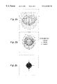
FIGS. 2a-2 c are spot diagrams illustrating the performance achieved in the spectral band of 3-5 micrometers; and
FIGS. 3a-3 c are spot diagrams illustrating the performance achieved in the spectral band of 8-12 micrometers.
DETAILED DESCRIPTION
The index of refraction of optical materials varies with wavelength. The refractive index is generally higher at shorter wavelengths so that light converges faster (the focal length is shorter) than at longer wavelengths. This spread in the focal position over a spectral range is the primary chromatic aberration called axial color. It is relatively easy to correct the axial color aberration in either the 3-5 or the 8-12 micrometer spectral range by simply combining low and high dispersion elements and dividing the magnification power of the lens system among positive and negative lens elements. Color correction of both bands is much more difficult.
The present inventor has discovered a unique combination of lens powers, including an aspheric surface, and materials that yield color correction for both spectral bands simultaneously. The type of lens and the materials are, in order of their appearance along a chief ray of a focal optical lens system, as follows:
Lens Material
Negative Zinc sulfide (ZnS)
Positive Zinc selenide (ZnSe)
Negative Gallium arsenide (GaAs)
Recent advances in the quantum well detectors, or any present or future detectors capable of dual spectral band imagery, give rise to a need for dual band optics such as disclosed herein so that such detectors can be utilized to their best efficiency.
An exemplary set of lens characteristics for a conventional quantum well detector is as follows:
Effective Focal Length (EFL) 7.5″
f/# 2.0
Field of View 4.0 × 4.0 degrees
Pixel Size 0.002″
Format Size 0.5 × 0.5
Spectral Range 3 to 5 μm and
8 to 12 μm
Cold Shield Efficiency 100%
To achieve the above characteristics, the simple lens triplet, while acceptable for some applications, does not provide optimum speed and field of view. Speed refers to the light gathering power of the lens. In commercial camera optics, this property of the lens system is indicated by the f/number. The exposure time required for a given photograph is proportional to the square of the f/number and will be shorter when a lens with a low f/number is used; thus, a lens having a higher speed reduces light gathering time.
Two widely spaced triplets in the form of a Petzval-type lens provide an optimum speed and field of view for the above-listed lens characteristics. A classic Petzval lens involves two spaced doublets, but the term is used here by analogy because each triplet is a net positive lens group.
The six element combination with two aspheric surfaces can be optimized on the ACCOSV optical design program. A resulting lens design shown in FIG. 1 and listed in Table 1 below.
TABLE 1
BASIC LENS DATA
Refrac.
Surf. Radius Thickness Medium Index Label
0 0.00000000 1.50000000E+20 AIR
1 0.00000000 −18.27594933 AIR
2 7.28700000 0.33000000 MATL C_ZnS 2.200833 10A
3 4.64064000 0.06544000 AIR 10B
4 5.14400000 0.98000000 MATL ZnSe 2.406485 11A
5 −33.65800000 0.05074000 AIR 11B
6 −21.27500000 0.28000000 MATL GaAs 3.277944 12A
7 33.65800000 4.27000000 AIR 12B
8 21.27500000 0.30000000 MATL C_ZnS 2.200833 13A
9 7.05700000 0.22000000 AIR 13B
10  5.14400000 0.52500000 MATL ZnSe 2.406485 14A
11  0.00000000 0.21700000 AIR 14B
12  2.20300000 0.22500000 MATL GaAs 3.277944 15A
13  1.90900000 1.01703000 AIR 15B
14  0.00000000 0.08000000 MATL ZnSe 2.406485 16A
15  0.00000000 0.10000000 MATL 16B
16* 0.00000000 2.50000000 AIR 17
17  0.00000000 0.00000000 AIR
CONIC CONSTANT (CC) AND ASPHERIC DATA
Surf. CC AD AE AF AG
3 0.00000E+00 −2.5363E−04 −1.59381E−05 −7.91405E−07 −6.71513E−08
9 0.00000E+00 9.85522E−04  3.35206E−05  7.40680E−06 −2.89437E−06
wherein AD, AE, AF and AG represent 4th, 6th, 8th and 10th order deformation coefficients, respectively and the asterisk * signifies where the aperture stop/cold shield is located.
REFRACTIVE INDICES
Surf. N1 N2 N3 N4 N5 ABBE
2 2.200833 2.212892 2.186965 1.000000 1.000000  46.316416
4 2.406485 2.412209 2.400068 1.000000 1.000000 115.848590
6 3.277944 3.282937 3.272502 1.000000 1.000000 218.286360
8 2.200833 2.212892 2.186965 1.000000 1.000000  46.316416
10  2.406485 2.412209 2.400068 1.000000 1.000000 115.848590
12  3.277944 3.282937 3.272502 1.000000 1.000000 218.286360
14  2.406485 2.412209 2.400068 1.000000 1.000000 115.848590
These refractive indices correspond to the 8-12 micrometer range and are different for the 3-5 micrometer range when generating the spot diagrams of FIGS. 2a-2 c.
WAVELENGTH DESIGNS
Wavelength # 1 2 3 4 5
Wavelength 10.00000 9.00000 11.00000 0.00000 0.00000
Spectral Weight 1.0000 1.0000  1.0000 1.0000  1.0000 
OPERATING CONDITIONS
Reference Object Reference Object Reference Image
Height Aperture Ht. Surface Surface Surface
−0.7336233+19 0.62393 0 16 17
(2.8000 Deg.)
APERTURE STOP AT SURFACE 15 (EN ADJUSTMENT)
Effective Focal Gauss Image
Length (EFL) Back Focus f/Number Length Height
7.4911 2.5000 2.00 8.6602 0.3662
STANDARD AND BOOLEAN APERTURE (TM) DATA (CA ON)
Surf. Type CAY CAX Y-OFFSET X-OFFSET LABEL
2 Cir. 2.54959 0.00000 0.00000 10A
3 Cir. 2.42975 0.00000 0.00000 10B
4 Cir. 2.43030 0.00000 0.00000 11A
5 Cir. 2.36548 0.00000 0.00000 11B
6 Cir. 2.36344 0.00000 0.00000 12A
7 Cir. 2.30949 0.00000 0.00000 12B
8 Cir. 1.43501 0.00000 0.00000 13A
9 Cir. 1.38404 0.00000 0.00000 13B
10  Cir. 1.37450 0.00000 0.00000 14A
11  Cir. 1.31524 0.00000 0.00000 14B
12  Cir. 1.08791 0.00000 0.00000 15A
13  Cir. 0.97822 0.00000 0.00000 15B
14  Cir. 0.68097 0.00000 0.00000 16A
15  Cir. 0.66855 0.00000 0.00000 16B
17  Cir. 0.37445 0.00000 0.00000
Lens units are inches.
Evaluation mode is focal.
Control wavelength is 1.
Naturally, other lens characteristics can be used within the scope of the present invention. The above data is exemplary and reflects an optimum lens data for a particular quantum well detector chip.
In the preferred embodiments of the present invention, in each lens triplet, a first lens 10, 13 is negative, a second lens 11, 14 is positive, and a third lens 12, 15 is negative as taken along the chief ray. Surfaces 10B and 13B of the ZNS lens are selected for receiving aspheric surfaces. ZnS is a diamond turnable lens material which greatly eases manufacturing requirements. Also, of the manufacturing methods available for making ZnS lenses, the Cleartran™ method provides a better, more homogenous material (C_ZnS) which is clearer in the 3-5 micrometer range than produced by some other methods.
As illustrated in FIG. 1, parallel light impinging on the Petzval lens system is focused on an image plane 18. A quantum well detector 19 can be placed at the image plane 18. A cryogenic vessel or Dewar houses the quantum well detector 19 to maintain the detector 19 at a temperature of approximately 77° Kelvin in order to increase detector sensitivity. The cold shield 20 of the Dewar is shown.
In these types of systems, optimum performance is achieved by cold shielding the detector array. This is done by introducing a cold diaphragm, or cold shield 20, with an aperture stop 17 in front of the detector array so that the viewing angle of the detector to the warm background is limited as nearly as possible to only that required for transmission of radiation from the scene. Since the amount of radiation reaching the detector from the cold shield 20 is negligible compared to the amount reaching the detector from the warm background of the field of view, induced noise in the detector is minimized. The cold shield 20 is typically placed within the Dewar. Also included in the optical system may be a Dewar window 16.
The performance achieved in each spectral band is shown by the spot diagrams in FIGS. 2a-2 c and 3 a-3 c. Rays representative of three wavelengths in each of the 3 to 5 and 8 to 12 spectral bands from an on-axis and two off-axis field points are distributed through the full aperture and are traced through the system, producing FIGS. 2c, 2 a and 2 b, respectively. In FIG. 2a, the FOB-Y is 1.0000 and the FOB-X is 0.0000; in FIG. 2b, the FOB-Y is 0.7000 and the FOB-X is 0.0000; in FIG. 2c, the FOB-Y is 0.0000 and the FOB-X is 0.0000; in FIG. 3a, the FOB-Y is 1.0000 and the FOB-X is 0.0000; in FIG. 3b, the FOB-Y is 0.7071 and the FOB-X is 0.0000; and in FIG. 3c, the FOB-Y is 0.0000 and the FOB-X is 0.0000, wherein FOB stands for fractional object height. FOB refers to the object point (or field angle when the object is at infinity) from which rays are traced.
As shown in FIGS. 2a-2 c and 3 a-3 c, the square in phantom is the pixel size of a typical quantum well detector, e.g., 50.8×50.8 micrometers (0.002 inches). In FIGS. 2a-2 c and 3 a-3 c, all spot diagram origins are on the chief ray. Since virtually all of the ray intercepts are contained within the pixel, the image resolution will be limited by such a detector.
By the above disclosed imaging system, the optimum capability of a quantum well detector can be utilized. A quantum well detector's capability could go under-utilized without an optical system such as disclosed herein that can simultaneously deliver the image quality required over both the 3 to 5 μm and 8 to 5 μm spectral bands. The lens system in accordance with the present invention yields excellent broadband color correction by a combination of infrared lens material suitable for tactical applications.
Certain preferred embodiments of the invention have been described by way of example. Various other embodiments and components thereof will be apparent, particularly in applying the lens triplets to perform various functions. Various parameters may be optimized for different purposes. For example, a beam splitter may be introduced into the lens system to split an image into the 3-5 μm range and the 8-12 μm range, whereupon the lens powers may vary and color correction requirements loosened because of the using more than one focal plane. The lens system can be useful with detectors capable of imaging either the 3 to 5 μm or 8 to 12 μm spectral bands, and an imaging system can be envisioned wherein high and low spectral band detectors can be selectively placed at the focal plane(s), by use of a beam splitter or employing a detector change-over mechanism. Naturally, optimum performance is achieved when employing a single detector capable of detecting both the 3 to 5 μm and 8 to spectral bands. The foregoing description is offered as illustrative and not limitative. Other variations and equivalents thereof are intended to be encompassed by the invention, which is defined by the claims appended hereto.

Claims (9)

I claim:
1. An optical imaging system comprising:
a lens system simultaneously focusing light in both the 3-5 and 8-12 micrometer spectral bands onto a single focal plane, wherein said lens system includes:
a first, negative zinc sulfide lens,
a second, positive zinc selenide lens, and
a third, negative gallium arsenide lens,
each of said first through third lenses being positioned along a chief ray and capable of simultaneous dual band imagery in both the 3-5 and 8-12 micrometer spectral bands; and
a detector, located at said single focal plane, capable of simultaneous dual band imagery in both the 3-5 and 8-12 micrometer spectral bands.
2. An optical imaging system according to claim 1, wherein said detector is a quantum well detector.
3. An optical imaging system according to claim 1, wherein said lens system further includes:
a fourth, negative zinc sulfide lens,
a fifth, positive zinc selenide lens,
a sixth, negative gallium arsenide lens,
each of said first through sixth lenses being positioned along a chief ray, said first through third and said fourth through sixth lenses forming two widely spaced triplets.
4. An optical imaging system according to claim 3, wherein said two widely spaced triplets form a Petzval-type lens.
5. An optical imaging system according to claim 3, wherein said lens system further includes a field flattener lens, and a cold shield diaphragm.
6. An optical imaging system according to claim 1, wherein at least one of said lenses has an aspheric surface.
7. An optical imaging system according to claim 6, wherein said aspheric surface is on said second zinc selenide lens.
8. An optical imaging system according to claim 3, wherein a surface on said fifth zinc selenide lens is aspheric.
9. An optical imaging system according to claim 3, wherein said lens system has the following basic lens data:
BASIC LENS DATA Refrac. Surf. Radius Thickness Medium Index 0 0.00000000 1.50000000E+20 AIR 1 0.00000000 −18.27594933 AIR 2 7.28700000 0.33000000 MATL C_ZnS 2.200833 3 4.64064000 0.06544000 AIR 4 5.14400000 0.98000000 MATL ZnSe 2.406485 5 −33.65800000 0.05074000 AIR 6 −21.27500000 0.28000000 MATL GaAs 3.277944 7 33.65800000 4.27000000 AIR 8 21.27500000 0.30000000 MATL C_ZnS 2.200833 9 7.05700000 0.22000000 AIR 10  5.14400000 0.52500000 MATL ZnSe 2.406485 11  0.00000000 0.21700000 AIR 12  2.20300000 0.22500000 MATL GaAs 3.277944 13  1.90900000 1.01703000 AIR 14  0.00000000 0.08000000 MATL ZnSe 2.406485 15  0.00000000 0.10000000 MATL 16  0.00000000 2.50000000 AIR 17  0.00000000 0.00000000 AIR
US08/310,108 1994-09-22 1994-09-22 Dual infrared band objective lens Expired - Fee Related US6423969B1 (en)

Priority Applications (2)

Application Number Priority Date Filing Date Title
US08/310,108 US6423969B1 (en) 1994-09-22 1994-09-22 Dual infrared band objective lens
US09/116,809 US7408159B1 (en) 1994-09-22 1998-08-07 Dual infrared band objective lens

Applications Claiming Priority (1)

Application Number Priority Date Filing Date Title
US08/310,108 US6423969B1 (en) 1994-09-22 1994-09-22 Dual infrared band objective lens

Related Child Applications (1)

Application Number Title Priority Date Filing Date
US09/116,809 Continuation US7408159B1 (en) 1994-09-22 1998-08-07 Dual infrared band objective lens

Publications (1)

Publication Number Publication Date
US6423969B1 true US6423969B1 (en) 2002-07-23

Family

ID=23201016

Family Applications (2)

Application Number Title Priority Date Filing Date
US08/310,108 Expired - Fee Related US6423969B1 (en) 1994-09-22 1994-09-22 Dual infrared band objective lens
US09/116,809 Expired - Fee Related US7408159B1 (en) 1994-09-22 1998-08-07 Dual infrared band objective lens

Family Applications After (1)

Application Number Title Priority Date Filing Date
US09/116,809 Expired - Fee Related US7408159B1 (en) 1994-09-22 1998-08-07 Dual infrared band objective lens

Country Status (1)

Country Link
US (2) US6423969B1 (en)

Cited By (12)

* Cited by examiner, † Cited by third party
Publication number Priority date Publication date Assignee Title
US6665116B1 (en) * 2000-07-10 2003-12-16 Hrl Laboratories, Llc Achromatic lens for millimeter-wave and infrared bands
US20050200946A1 (en) * 2004-03-09 2005-09-15 Bryant Kyle R. Miniature high-resolution multi-spectral objective lens
US20050243411A1 (en) * 2004-05-03 2005-11-03 Cook Lacy G Dual-band, dual-focal-length, relayed refractive imager
US20070183024A1 (en) * 2006-02-03 2007-08-09 John Tejada Dual band lens system incorporating molded chalcogenide
US20070195403A1 (en) * 2006-02-03 2007-08-23 John Tejada Method and system for simultaneously imaging in the near infrared and short wave infrared spectrums
US7339741B1 (en) * 2006-11-14 2008-03-04 Northrop Grumman Systems Corporation Multi-color wide angle infrared optical systems and methods
US20090027766A1 (en) * 2006-01-30 2009-01-29 Tatsuya Izumi Infrared lens, infrared camera and night vision
CN102289056A (en) * 2011-09-27 2011-12-21 苏州大学 Front objective lens with large field of view and large relative aperture for imaging spectrograph
US20120026382A1 (en) * 2010-07-30 2012-02-02 Raytheon Company Wide field of view lwir high speed imager
EP2792991A3 (en) * 2013-04-20 2015-01-21 Diehl BGT Defence GmbH & Co.KG Seeker for a guided missile
US20160116719A1 (en) * 2014-10-27 2016-04-28 Qioptiq Limited Compact multispectral wide angle refractive optical system
WO2019032158A3 (en) * 2017-07-20 2019-05-09 Raytheon Company Two-color inverse telephoto refractive optical form with external pupil for cold shielding

Families Citing this family (4)

* Cited by examiner, † Cited by third party
Publication number Priority date Publication date Assignee Title
US8294988B2 (en) * 2010-09-02 2012-10-23 Raytheon Company Dual field of view refractive optical system with external pupil and internal stabilization
US10095008B1 (en) 2015-11-24 2018-10-09 Lockhead Martin Corporation Lens assembly with switched ultra-narrow field-of-view configuration
CN105319669B (en) * 2015-12-02 2017-12-26 中国航空工业集团公司洛阳电光设备研究所 A kind of two-waveband infrared optical system
US10317650B1 (en) 2016-11-21 2019-06-11 Lockheed Martin Corporation Infrared imaging system with an athermalized dual-band ultra-WFOV optical system and method

Citations (12)

* Cited by examiner, † Cited by third party
Publication number Priority date Publication date Assignee Title
US4486069A (en) * 1981-07-01 1984-12-04 Barr & Stroud Limited Afocal telescopes
US4537464A (en) * 1982-06-25 1985-08-27 Kern & Co. Ltd. Infrared objective system lens
US4586069A (en) 1982-09-14 1986-04-29 Messershmitt-Boelkow-Blohm Gesellschaft-Mit-Beschraenkter Haftung Opto-electrical device made of silicon for detecting infrared light
US4621888A (en) * 1983-03-10 1986-11-11 Texas Instruments Incorporated Coaxial wideband refractive optical system
US4714307A (en) 1985-07-13 1987-12-22 Pilkington P.E. Limited Catadioptric infrared lenses
US4871219A (en) 1987-11-19 1989-10-03 Texas Instruments Incorporated Wide spectral band infrared refractive lens
US4903101A (en) 1988-03-28 1990-02-20 California Institute Of Technology Tunable quantum well infrared detector
US4921318A (en) 1987-06-27 1990-05-01 Gec-Marconi Limited Lens systems
US4975567A (en) 1989-06-29 1990-12-04 The United States Of America As Represented By The Secretary Of The Navy Multiband photoconductive detector based on layered semiconductor quantum wells
US4989962A (en) 1988-10-31 1991-02-05 Hughes Aircraft Company Dual band/dual FOV infrared telescope
US4999005A (en) 1988-10-19 1991-03-12 Cooper Erwin E Wide band color correcting infrared lens system
US5198659A (en) 1992-03-23 1993-03-30 The United States Of America As Represented By The Secretary Of The Army Wide-range multicolor IR detector

Patent Citations (12)

* Cited by examiner, † Cited by third party
Publication number Priority date Publication date Assignee Title
US4486069A (en) * 1981-07-01 1984-12-04 Barr & Stroud Limited Afocal telescopes
US4537464A (en) * 1982-06-25 1985-08-27 Kern & Co. Ltd. Infrared objective system lens
US4586069A (en) 1982-09-14 1986-04-29 Messershmitt-Boelkow-Blohm Gesellschaft-Mit-Beschraenkter Haftung Opto-electrical device made of silicon for detecting infrared light
US4621888A (en) * 1983-03-10 1986-11-11 Texas Instruments Incorporated Coaxial wideband refractive optical system
US4714307A (en) 1985-07-13 1987-12-22 Pilkington P.E. Limited Catadioptric infrared lenses
US4921318A (en) 1987-06-27 1990-05-01 Gec-Marconi Limited Lens systems
US4871219A (en) 1987-11-19 1989-10-03 Texas Instruments Incorporated Wide spectral band infrared refractive lens
US4903101A (en) 1988-03-28 1990-02-20 California Institute Of Technology Tunable quantum well infrared detector
US4999005A (en) 1988-10-19 1991-03-12 Cooper Erwin E Wide band color correcting infrared lens system
US4989962A (en) 1988-10-31 1991-02-05 Hughes Aircraft Company Dual band/dual FOV infrared telescope
US4975567A (en) 1989-06-29 1990-12-04 The United States Of America As Represented By The Secretary Of The Navy Multiband photoconductive detector based on layered semiconductor quantum wells
US5198659A (en) 1992-03-23 1993-03-30 The United States Of America As Represented By The Secretary Of The Army Wide-range multicolor IR detector

Non-Patent Citations (3)

* Cited by examiner, † Cited by third party
Title
M. Roberts et al., "Wide waveband infrared optics," Proceedings SPIE, vol. 1013, 1988, pp. 84-91.
M.O. Lidwell, "Achromatism of lenses for thermal IR," Proceedings SPIE, vol. 518, 1984, pp. 73-80.
T.H. Jamieson, "Ultrawide waveband optics," Optical Engineering, Mar./Apr. 1984, vol. 23, No. 2, pp. 111-116.

Cited By (25)

* Cited by examiner, † Cited by third party
Publication number Priority date Publication date Assignee Title
US6665116B1 (en) * 2000-07-10 2003-12-16 Hrl Laboratories, Llc Achromatic lens for millimeter-wave and infrared bands
US20040130780A1 (en) * 2000-07-10 2004-07-08 Harvey Robin J. Method for making an achromatic lens for millimeter-wave and infrared bands
US7088503B2 (en) * 2000-07-10 2006-08-08 Hrl Lab Llc Method for making an achromatic lens for millimeter-wave and infrared bands
US20050200946A1 (en) * 2004-03-09 2005-09-15 Bryant Kyle R. Miniature high-resolution multi-spectral objective lens
US6999231B2 (en) * 2004-03-09 2006-02-14 The United States Of America As Represented By The Secretary Of The Army Miniature high-resolution multi-spectral objective lens
US20050243411A1 (en) * 2004-05-03 2005-11-03 Cook Lacy G Dual-band, dual-focal-length, relayed refractive imager
US7218444B2 (en) 2004-05-03 2007-05-15 Raytheon Company Dual-band, dual-focal-length, relayed refractive imager
US20090027766A1 (en) * 2006-01-30 2009-01-29 Tatsuya Izumi Infrared lens, infrared camera and night vision
US7738169B2 (en) * 2006-01-30 2010-06-15 Sumitomo Electric Industries, Ltd. Infrared lens, infrared camera and night vision
US20100187418A1 (en) * 2006-01-30 2010-07-29 Sumitomo Electric Industries, Ltd. Infrared lens, infrared camera, and night vision
US7911688B2 (en) 2006-01-30 2011-03-22 Sumitomo Electric Industries, Ltd. Infrared lens, infrared camera, and night vision
US8085465B2 (en) 2006-01-30 2011-12-27 Sumitomo Electric Industries, Ltd. Infrared lens, infrared camera, and night vision
US7280273B2 (en) * 2006-02-03 2007-10-09 Janos Technology Inc. Method and system for simultaneously imaging in the near infrared and short wave infrared spectrums
US7369303B2 (en) 2006-02-03 2008-05-06 Janos Technology Inc. Dual band lens system incorporating molded chalcogenide
US20070183024A1 (en) * 2006-02-03 2007-08-09 John Tejada Dual band lens system incorporating molded chalcogenide
US20070195403A1 (en) * 2006-02-03 2007-08-23 John Tejada Method and system for simultaneously imaging in the near infrared and short wave infrared spectrums
US7339741B1 (en) * 2006-11-14 2008-03-04 Northrop Grumman Systems Corporation Multi-color wide angle infrared optical systems and methods
US8279520B2 (en) * 2010-07-30 2012-10-02 Raytheon Company Wide field of view LWIR high speed imager
US20120026382A1 (en) * 2010-07-30 2012-02-02 Raytheon Company Wide field of view lwir high speed imager
CN102289056A (en) * 2011-09-27 2011-12-21 苏州大学 Front objective lens with large field of view and large relative aperture for imaging spectrograph
CN102289056B (en) * 2011-09-27 2013-03-06 苏州大学 Front objective lens with large field of view and large relative aperture for imaging spectrograph
EP2792991A3 (en) * 2013-04-20 2015-01-21 Diehl BGT Defence GmbH & Co.KG Seeker for a guided missile
US20160116719A1 (en) * 2014-10-27 2016-04-28 Qioptiq Limited Compact multispectral wide angle refractive optical system
WO2019032158A3 (en) * 2017-07-20 2019-05-09 Raytheon Company Two-color inverse telephoto refractive optical form with external pupil for cold shielding
US10670841B2 (en) 2017-07-20 2020-06-02 Raytheon Company Two-color inverse telephoto refractive optical form with external pupil for cold shielding

Also Published As

Publication number Publication date
US7408159B1 (en) 2008-08-05

Similar Documents

Publication Publication Date Title
US4431917A (en) Compact, high cold shield efficiency optical system
US6423969B1 (en) Dual infrared band objective lens
US6903343B2 (en) Lightweight laser designator ranger flir optics
US6919988B2 (en) Optical system for simultaneous imaging of LWIR and millimeter wave radiation
US5229880A (en) Three field of view refractive afocal telescope
US5140459A (en) Apparatus and method for optical relay and reimaging
US8101918B1 (en) Re-imaging infrared lenses
US5838489A (en) Refractive broad band IR objective
US20070195403A1 (en) Method and system for simultaneously imaging in the near infrared and short wave infrared spectrums
KR101807414B1 (en) Long Range Oblique Photography Camera Optical System for Simultaneous Shooting of Triple Band Wavelength Image
US5548439A (en) Three field of view refractive infrared telescope with fixed medium filed of view
EP0045138B1 (en) Infra-red optical system
Jeong et al. Infrared dual-field-of-view optical system design with electro-optic/laser common-aperture optics
US8937764B2 (en) Optical system with off-axis packaged illuminator
EP3015902B1 (en) Compact multispectral wide angle refractive optical system
CA2466788C (en) Optical apparatus
JP2737272B2 (en) Variable power optical system for infrared
EP3642657B1 (en) Wide angle mwir f-theta lens
CN107121760A (en) A kind of infrared refractive and reflective panorama camera lens of broadband refrigeration
GB2433608A (en) Ancillary optical system for imaging optics in the infrared spectral region
CA3055136C (en) Orthoscopic projection lens
GB2247090A (en) Flat-field scanner
US20230168475A1 (en) Anti-blur infrared lens for panoramic camera system using hd resolution sensor
Ming et al. Optical system design of four-channel dual-band infrared panoramic imaging
RU2815391C1 (en) Two-channel mirror lens system

Legal Events

Date Code Title Description
AS Assignment

Owner name: MARTIN MARIETTA CORPORATION, MARYLAND

Free format text: ASSIGNMENT OF ASSIGNORS INTEREST;ASSIGNOR:AMON, MAX;REEL/FRAME:007172/0081

Effective date: 19940919

AS Assignment

Owner name: LOCKHEED MARTIN CORPORATION, MARYLAND

Free format text: ASSIGNMENT OF ASSIGNORS INTEREST;ASSIGNOR:MARTIN MARIETTA CORPORATION;REEL/FRAME:012818/0294

Effective date: 19960128

FPAY Fee payment

Year of fee payment: 4

FPAY Fee payment

Year of fee payment: 8

REMI Maintenance fee reminder mailed
LAPS Lapse for failure to pay maintenance fees
STCH Information on status: patent discontinuation

Free format text: PATENT EXPIRED DUE TO NONPAYMENT OF MAINTENANCE FEES UNDER 37 CFR 1.362

FP Lapsed due to failure to pay maintenance fee

Effective date: 20140723