US6414830B1 - ESD protection circuit for integrated circuit with operating voltages exceeding power supply voltages - Google Patents
ESD protection circuit for integrated circuit with operating voltages exceeding power supply voltages Download PDFInfo
- Publication number
- US6414830B1 US6414830B1 US09/365,458 US36545899A US6414830B1 US 6414830 B1 US6414830 B1 US 6414830B1 US 36545899 A US36545899 A US 36545899A US 6414830 B1 US6414830 B1 US 6414830B1
- Authority
- US
- United States
- Prior art keywords
- circuit
- circuit node
- type
- contact region
- mos transistor
- Prior art date
- Legal status (The legal status is an assumption and is not a legal conclusion. Google has not performed a legal analysis and makes no representation as to the accuracy of the status listed.)
- Expired - Fee Related
Links
- 239000004065 semiconductor Substances 0.000 claims abstract description 68
- 239000000758 substrate Substances 0.000 claims description 39
- 230000015556 catabolic process Effects 0.000 description 2
- 238000010586 diagram Methods 0.000 description 2
- 230000004048 modification Effects 0.000 description 2
- 238000012986 modification Methods 0.000 description 2
Images


Classifications
-
- H—ELECTRICITY
- H10—SEMICONDUCTOR DEVICES; ELECTRIC SOLID-STATE DEVICES NOT OTHERWISE PROVIDED FOR
- H10D—INORGANIC ELECTRIC SEMICONDUCTOR DEVICES
- H10D89/00—Aspects of integrated devices not covered by groups H10D84/00 - H10D88/00
- H10D89/60—Integrated devices comprising arrangements for electrical or thermal protection, e.g. protection circuits against electrostatic discharge [ESD]
- H10D89/601—Integrated devices comprising arrangements for electrical or thermal protection, e.g. protection circuits against electrostatic discharge [ESD] for devices having insulated gate electrodes, e.g. for IGFETs or IGBTs
- H10D89/711—Integrated devices comprising arrangements for electrical or thermal protection, e.g. protection circuits against electrostatic discharge [ESD] for devices having insulated gate electrodes, e.g. for IGFETs or IGBTs using bipolar transistors as protective elements
- H10D89/713—Integrated devices comprising arrangements for electrical or thermal protection, e.g. protection circuits against electrostatic discharge [ESD] for devices having insulated gate electrodes, e.g. for IGFETs or IGBTs using bipolar transistors as protective elements including a PNP transistor and a NPN transistor, wherein each of said transistors has its base region coupled to the collector region of the other transistor, e.g. silicon controlled rectifier [SCR] devices
Definitions
- the present invention generally relates to protection circuitry for integrated circuits. More particularly, the present invention relates to an ESD protection circuit suitable for an integrated circuit with input voltages beyond power supply voltage range.
- CMOS integrated circuits In sub-micron CMOS integrated circuits (ICs), is electrostatic discharge, ESD hereinafter, is a reliability concern.
- ESD electrostatic discharge
- FIG. 1 a conventional ESD protection circuit fabricated onto a semiconductor substrate is schematically illustrated in a cross-sectional view.
- the fabricated ESD protection circuit is a lateral semiconductor controlled rectifier.
- reference numeral 1 designates a core circuit or an internal circuit for an integrated circuit, the core circuit 1 being powered by voltage sources V SS and V DD while operating.
- Reference numeral 2 represents a bonding pad to which the lateral semiconductor controlled rectifier 3 is electrically connected.
- the lateral semiconductor controlled rectifier 3 can turn on to bypass the ESD stress occurring at the bonding pad and thus protect the core circuit 1 from ESD damage.
- an n-well 11 is formed on a p-type semiconductor substrate 10 .
- a p + doped region 12 is formed in the n-well 11 as an anode of the lateral semiconductor controlled rectifier 3
- an n + doped region 13 is formed in the p-type substrate 10 as a cathode of the lateral semiconductor controlled rectifier 3 .
- an n + contact region 14 and a p + contact region 15 are formed in the n-well 11 and the p-type substrate 10 , respectively.
- the lateral semiconductor controlled rectifier 3 can be considered as two bipolar transistors T 1 and T 2 .
- the pnp transistor T 1 is formed by the anode (p + doped region 12 ) as an emitter, the n-well 11 as a base, and the p-type substrate 10 as a collector.
- the npn transistor T 2 is formed by the cathode (n + doped region 13 ) as an emitter, the p-type substrate 10 as a base, and the n-well 11 as a collector.
- R well and R sub denote the spreading resistances of the n-well 11 and the p-type substrate 10 , respectively.
- the p + doped region 12 and the n + contact region 14 are tied together to the bonding pad 2
- the n + doped region 13 and the p + contact region 15 are tied together to V SS , which is grounded under circuit operation.
- the V SS and V DD are not powered, that is, the nodes is floating. If the ESD stress is relatively positive to V SS the junction between the n-well 11 and p-type substrate 10 enters avalanche breakdown to trigger the lateral semiconductor controlled rectifier 3 , where the trigger voltage and the trigger current are denoted by V trig and I trig , respectively. Therefore, the lateral semiconductor controlled rectifier 3 turns on to conduct a current bypassing the ESD stress, and thus clamp the potential between the anode 12 and the cathode 13 at a holding voltage V h so as to protect the core circuit 1 from ESD damage.
- the junction between the n-well 11 and p-type substrate 10 is forward-biased to protect the core circuit 1 from ESD damage as well.
- the I-V characteristic curve of the lateral semiconductor controlled rectifier 3 is shown in FIG. 2 .
- I/O pins having operational voltages that exceed the range between V SS and V DD under circuit operation.
- the junction between the n-well 11 and the p-type substrate 10 will be forward-biased so that the performance of the core circuit 1 is affected.
- an object of the present invention to provide an ESD protection circuit for an integrated circuit with operating voltages exceeding power supply voltages, which can be turned off under circuit operation without disturbing circuit performance.
- the present invention provides an ESD protection circuit having a semiconductor controlled rectifier and an MOS transistor.
- the semiconductor is controlled rectifier has an anode and a cathode connected to a first circuit node and a second circuit node, respectively.
- the MOS transistor is connected between the anode and an anode gate of the semiconductor controlled rectifier to increase the magnitude of a turn-on voltage at which the semiconductor controlled rectifier enters a negative forward bias.
- the present invention provides an ESD protection circuit comprising a p-type semiconductor layer having a first contact region, an n-type semiconductor layer having a second contact region, an MOS transistor, and an n-type doped region.
- the n-type semiconductor layer is in contact with the p-type semiconductor layer to establish a junction therebetween.
- the MOS transistor is formed in the n-type semiconductor layer with one source/drain region connected to a first circuit node and another source/drain region connected to the second contact region.
- the n-type doped region is formed in the p-type semiconductor layer and connected with the first contact region to a second circuit node.
- the ESD protection of the present invention can be used on those I/O pins having operational voltages that greater than V DD or even less than V SS to ensure that the MOS transistor can turn off under circuit operation without disturbing circuit performance.
- the potential between the first and second circuit nodes can still be clamped by the semiconductor controlled rectifier to a low voltage so as to protect a core circuit of an integrated circuit from ESD damage.
- FIG. 1 schematically illustrates a conventional ESD protection circuit fabricated onto a semiconductor substrate in a cross-sectional view
- FIG. 2 depicts the I-V characteristic curve of the conventional ESD protection circuit of FIG. 1;
- FIG. 3 schematically illustrates an ESD protection circuit in accordance with a first preferred embodiment of the present invention fabricated onto a semiconductor substrate in a cross-sectional view;
- FIG. 4 depicts the equivalent circuit diagram of FIG. 3
- FIG. 5 depicts the I-V characteristic curve of FIG. 3
- FIG. 6 schematically illustrates an ESD protection circuit in accordance with a second preferred embodiment of the present invention fabricated onto a semiconductor substrate in a cross-sectional view;
- FIG. 7 schematically illustrates an ESD protection circuit in accordance with a third preferred embodiment of the present invention fabricated onto a semiconductor substrate in a cross-sectional view.
- FIG. 8 schematically illustrates an ESD protection circuit in accordance with a fourth preferred embodiment of the present invention fabricated onto a semiconductor substrate in a cross-sectional view.
- FIG. 4 depicts the equivalent circuit diagram of FIG. 3 .
- reference numeral 1 designates a core circuit or an internal circuit for an integrated circuit, the core circuit 1 being powered by two voltage sources V SS and V DD .
- Reference numeral 2 represents a bonding pad to which the ESD protection circuit 4 of the present invention is electrically connected.
- the ESD protection circuit 4 is employed to bypass ESD stress occurring at the bonding pad 2 and thus protect the core circuit 1 from ESD damage.
- the ESD protection circuit 4 comprises a lateral semiconductor controlled rectifier 40 and an MOS transistor 41 .
- an n-well 21 is formed on a p-type semiconductor substrate 20 .
- a p + doped region 22 is formed in the n-well 21 as an anode of the lateral semiconductor controlled rectifier 40
- an n + doped region 23 is formed in the p-type substrate 20 as a cathode of the lateral semiconductor controlled rectifier 40 .
- the n-well 21 and p-type substrate 20 serve as an anode gate and a cathode gate for the lateral semiconductor controlled rectifier 40 , respectively.
- an n + contact region 24 and a p + contact region 25 are formed within the n-well 21 and the p-type substrate 20 , respectively.
- a p + doped region 26 is provided between the p ⁇ doped region 22 and the n + contact region 24 .
- a gate structure 27 is formed to overlie a portion of the n-well 21 between the p + doped region 22 and the p + doped region 26 as shown in FIG. 3 .
- the gate structure 27 includes an dielectric layer and an electrode layer.
- the dielectric layer can be of field oxide or thick oxide.
- the lateral semiconductor controlled rectifier 40 can be considered as two bipolar transistors T 3 and T 4 .
- the pnp transistor T 3 is formed by the anode (p + doped region 22 ) as an emitter, the n-well 21 as a base, and the p-type substrate 20 as a collector.
- the npn transistor T 4 is formed by the cathode (n ⁇ doped region 23 ) as an emitter, the p-type substrate 20 as a base, and the n-well 21 as a collector.
- R well and R sub denote the spreading resistances of the n-well 21 and the p-type substrate 20 , respectively.
- the p + doped region 22 , the gate structure 27 , and the p + doped region 26 serve as the drain, gate, and source of the MOS transistor 41 , respectively, while the n-well 21 serves as the bulk of the MOS transistor 41 .
- the MOS transistor 41 should be provided with a high threshold voltage, for example,
- the MOS transistor 41 can be a thick oxide device or a field device.
- the p + doped region 22 and the gate structure 27 are tied together to the bonding pad 2
- the p + doped region 26 and n + contact region 24 are tied together
- the n + doped region 23 and the p ⁇ contact region 25 are tied together to V SS .
- the MOS transistor 41 When ESD stress positive to V SS occurs to the bonding pad 2 , the MOS transistor 41 turns off and the junction between the n-well 21 and p-type substrate 20 enters avalanche breakdown to trigger the lateral semiconductor controlled rectifier 41 . Therefore, the lateral semiconductor controlled rectifier 41 can turn on to conduct a current from the p + doped region 22 , through the n-well 21 and p-type substrate 20 , to the n + doped region 23 . Thus, the potential between the potential between the anode 22 and the cathode 23 can be clamped at a holding voltage V h so as to protect the core circuit 1 from ESD damage.
- the I-V characteristic curve of the ESD protection circuit 4 in accordance with one preferred embodiment of the present invention is shown in FIG. 5 . Note that the turn-on voltage at which the junction between the n-well 21 and p-type substrate 20 is forward-biased negatively can be less than ⁇ 10V.
- V DD is powered (for example by 5V or 3.3V) and V SS is grounded.
- V SS is grounded.
- the ESD protection circuit 4 of the present invention can ensure that the lateral semiconductor controlled rectifier 41 can turn off due to the trigger voltage thereof greater than 10V.
- the ESD protection circuit 4 of the present invention can ensure that threshold voltage is less than ⁇ 10V, therefore not disturbing circuit performance.
- the ESD protection can be used on those I/O pins having operational voltages greater than V DD or even less than V SS to ensure that the ESD protection circuit 4 can turn off under circuit operation without disturbing circuit performance.
- the potential between the bonding pad 2 and V SS can still be clamped to a low voltage so as to protect the core circuit 1 from ESD damage.
- V SS is coupled to the gate structure 27 through an inverter 60 .
- an ESD protection circuit in accordance with a third preferred embodiment of the present invention fabricated onto a semiconductor substrate is schematically illustrated in a cross-sectional view.
- the p + doped region 22 of FIG. 3 is divided into two p + doped regions 70 and 71 formed in n-wells 72 and 73 , respectively.
- the p + doped regions 70 and 71 are tied together.
- the MOS transistor 40 is formed within the n-well 73 , as are the p + doped region 26 and the n + contact region 24 .
- the gate structure 27 is formed to cover a portion of the n-well 73 between the p + doped regions 71 an 26 .
- FIG. 8 schematically illustrates an ESD protection circuit in accordance with a fourth preferred embodiment of the present invention fabricated onto a semiconductor substrate in a cross-sectional view.
- the p + doped region 22 of FIG. 3 is divided into two p + doped regions 80 and 81 formed in n-wells 82 and 83 , respectively.
- the p + doped regions 80 and 81 are tied together.
- the n + doped region 24 is formed in other n-well 84 , individually.
- the MOS transistor 40 is formed in the n-well 83 thereby forming the p + doped region 26 within the n-well 83 and forming the gate structure 27 overlying a portion of the n-well 83 between the p + doped regions 81 an 26 .
Landscapes
- Semiconductor Integrated Circuits (AREA)
- Metal-Oxide And Bipolar Metal-Oxide Semiconductor Integrated Circuits (AREA)
Abstract
An ESD protection circuit comprises a semiconductor controlled rectifier and an MOS transistor. The semiconductor controlled rectifier has an anode and a cathode connected to a first circuit node and a second circuit node, respectively. The MOS transistor is connected between the anode and an anode gate of the semiconductor controlled rectifier to increase the magnitude of a turn-on voltage at which the semiconductor controlled rectifier enters a negative forward bias.
Description
1. Field of the Invention
The present invention generally relates to protection circuitry for integrated circuits. More particularly, the present invention relates to an ESD protection circuit suitable for an integrated circuit with input voltages beyond power supply voltage range.
2. Description of the Related Art
In sub-micron CMOS integrated circuits (ICs), is electrostatic discharge, ESD hereinafter, is a reliability concern. Referring to FIG. 1, a conventional ESD protection circuit fabricated onto a semiconductor substrate is schematically illustrated in a cross-sectional view. The fabricated ESD protection circuit is a lateral semiconductor controlled rectifier. In the drawing, reference numeral 1 designates a core circuit or an internal circuit for an integrated circuit, the core circuit 1 being powered by voltage sources VSS and VDD while operating. Reference numeral 2 represents a bonding pad to which the lateral semiconductor controlled rectifier 3 is electrically connected. During an ESD event, the lateral semiconductor controlled rectifier 3 can turn on to bypass the ESD stress occurring at the bonding pad and thus protect the core circuit 1 from ESD damage.
As shown in FIG. 1, an n-well 11 is formed on a p-type semiconductor substrate 10. A p+ doped region 12 is formed in the n-well 11 as an anode of the lateral semiconductor controlled rectifier 3, while an n+ doped region 13 is formed in the p-type substrate 10 as a cathode of the lateral semiconductor controlled rectifier 3. Moreover, an n+ contact region 14 and a p+ contact region 15 are formed in the n-well 11 and the p-type substrate 10, respectively.
The lateral semiconductor controlled rectifier 3 can be considered as two bipolar transistors T1 and T2. As shown in FIG. 1, the pnp transistor T1 is formed by the anode (p+ doped region 12) as an emitter, the n-well 11 as a base, and the p-type substrate 10 as a collector. The npn transistor T2 is formed by the cathode (n+ doped region 13) as an emitter, the p-type substrate 10 as a base, and the n-well 11 as a collector. Moreover, Rwell and Rsub denote the spreading resistances of the n-well 11 and the p-type substrate 10, respectively. In FIG. 1, the p+ doped region 12 and the n+ contact region 14 are tied together to the bonding pad 2, the n+ doped region 13 and the p+ contact region 15 are tied together to VSS, which is grounded under circuit operation.
When ESD stress occurs to the bonding pad 2, the VSS and VDD are not powered, that is, the nodes is floating. If the ESD stress is relatively positive to VSS the junction between the n-well 11 and p-type substrate 10 enters avalanche breakdown to trigger the lateral semiconductor controlled rectifier 3, where the trigger voltage and the trigger current are denoted by Vtrig and Itrig, respectively. Therefore, the lateral semiconductor controlled rectifier 3 turns on to conduct a current bypassing the ESD stress, and thus clamp the potential between the anode 12 and the cathode 13 at a holding voltage Vh so as to protect the core circuit 1 from ESD damage. If the ESD stress is relatively negative to VSS, the junction between the n-well 11 and p-type substrate 10 is forward-biased to protect the core circuit 1 from ESD damage as well. The I-V characteristic curve of the lateral semiconductor controlled rectifier 3 is shown in FIG. 2.
However, some specific integrated circuits are provided with I/O pins having operational voltages that exceed the range between VSS and VDD under circuit operation. In other words, there are some signals having a potential greater than VDD or less than VSS. However, when the signal with a potential lower s than VSS is provided, the junction between the n-well 11 and the p-type substrate 10 will be forward-biased so that the performance of the core circuit 1 is affected.
Therefore, it is an object of the present invention to provide an ESD protection circuit for an integrated circuit with operating voltages exceeding power supply voltages, which can be turned off under circuit operation without disturbing circuit performance.
For achieving the above-identified object, the present invention provides an ESD protection circuit having a semiconductor controlled rectifier and an MOS transistor. The semiconductor is controlled rectifier has an anode and a cathode connected to a first circuit node and a second circuit node, respectively. The MOS transistor is connected between the anode and an anode gate of the semiconductor controlled rectifier to increase the magnitude of a turn-on voltage at which the semiconductor controlled rectifier enters a negative forward bias.
Moreover, the present invention provides an ESD protection circuit comprising a p-type semiconductor layer having a first contact region, an n-type semiconductor layer having a second contact region, an MOS transistor, and an n-type doped region. The n-type semiconductor layer is in contact with the p-type semiconductor layer to establish a junction therebetween. The MOS transistor is formed in the n-type semiconductor layer with one source/drain region connected to a first circuit node and another source/drain region connected to the second contact region. The n-type doped region is formed in the p-type semiconductor layer and connected with the first contact region to a second circuit node.
Accordingly, the ESD protection of the present invention can be used on those I/O pins having operational voltages that greater than VDD or even less than VSS to ensure that the MOS transistor can turn off under circuit operation without disturbing circuit performance. During an ESD event, the potential between the first and second circuit nodes can still be clamped by the semiconductor controlled rectifier to a low voltage so as to protect a core circuit of an integrated circuit from ESD damage.
The following detailed description, given by way of examples and not intended to limit the invention to the embodiments described herein, will best be understood in conjunction with the accompanying drawings, in which:
FIG. 1 schematically illustrates a conventional ESD protection circuit fabricated onto a semiconductor substrate in a cross-sectional view;
FIG. 2 depicts the I-V characteristic curve of the conventional ESD protection circuit of FIG. 1;
FIG. 3 schematically illustrates an ESD protection circuit in accordance with a first preferred embodiment of the present invention fabricated onto a semiconductor substrate in a cross-sectional view;
FIG. 4 depicts the equivalent circuit diagram of FIG. 3;
FIG. 5 depicts the I-V characteristic curve of FIG. 3;
FIG. 6 schematically illustrates an ESD protection circuit in accordance with a second preferred embodiment of the present invention fabricated onto a semiconductor substrate in a cross-sectional view;
FIG. 7 schematically illustrates an ESD protection circuit in accordance with a third preferred embodiment of the present invention fabricated onto a semiconductor substrate in a cross-sectional view; and
FIG. 8 schematically illustrates an ESD protection circuit in accordance with a fourth preferred embodiment of the present invention fabricated onto a semiconductor substrate in a cross-sectional view.
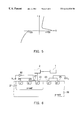
Referring to FIG. 3, an ESD protection circuit in accordance with a first preferred embodiment of the present invention fabricated onto a semiconductor substrate is schematically illustrated in a cross-sectional view. FIG. 4 depicts the equivalent circuit diagram of FIG. 3. In the drawing, reference numeral 1 designates a core circuit or an internal circuit for an integrated circuit, the core circuit 1 being powered by two voltage sources VSS and VDD. Reference numeral 2 represents a bonding pad to which the ESD protection circuit 4 of the present invention is electrically connected. During an ESD event the ESD protection circuit 4 is employed to bypass ESD stress occurring at the bonding pad 2 and thus protect the core circuit 1 from ESD damage. According to the present invention, the ESD protection circuit 4 comprises a lateral semiconductor controlled rectifier 40 and an MOS transistor 41.
In FIG. 3, an n-well 21 is formed on a p-type semiconductor substrate 20. A p+ doped region 22 is formed in the n-well 21 as an anode of the lateral semiconductor controlled rectifier 40, while an n+ doped region 23 is formed in the p-type substrate 20 as a cathode of the lateral semiconductor controlled rectifier 40. In addition, the n-well 21 and p-type substrate 20 serve as an anode gate and a cathode gate for the lateral semiconductor controlled rectifier 40, respectively. Moreover, an n+ contact region 24 and a p+ contact region 25 are formed within the n-well 21 and the p-type substrate 20, respectively.
According to the present invention, a p+ doped region 26 is provided between the p− doped region 22 and the n+ contact region 24. A gate structure 27 is formed to overlie a portion of the n-well 21 between the p+ doped region 22 and the p+ doped region 26 as shown in FIG. 3. Typically, the gate structure 27 includes an dielectric layer and an electrode layer. Preferably, the dielectric layer can be of field oxide or thick oxide.
The lateral semiconductor controlled rectifier 40 can be considered as two bipolar transistors T3 and T4. In FIG. 1, the pnp transistor T3 is formed by the anode (p+ doped region 22) as an emitter, the n-well 21 as a base, and the p-type substrate 20 as a collector. The npn transistor T4 is formed by the cathode (n− doped region 23) as an emitter, the p-type substrate 20 as a base, and the n-well 21 as a collector. Moreover, Rwell and Rsub denote the spreading resistances of the n-well 21 and the p-type substrate 20, respectively.
Furthermore, the p+ doped region 22, the gate structure 27, and the p+ doped region 26 serve as the drain, gate, and source of the MOS transistor 41, respectively, while the n-well 21 serves as the bulk of the MOS transistor 41. It is noted that the MOS transistor 41 should be provided with a high threshold voltage, for example, |VT|>10V. Preferably, the MOS transistor 41 can be a thick oxide device or a field device.
In this embodiment, the p+ doped region 22 and the gate structure 27 are tied together to the bonding pad 2, the p+ doped region 26 and n+ contact region 24 are tied together, and the n+ doped region 23 and the p− contact region 25 are tied together to VSS.
When ESD stress positive to VSS occurs to the bonding pad 2, the MOS transistor 41 turns off and the junction between the n-well 21 and p-type substrate 20 enters avalanche breakdown to trigger the lateral semiconductor controlled rectifier 41. Therefore, the lateral semiconductor controlled rectifier 41 can turn on to conduct a current from the p+ doped region 22, through the n-well 21 and p-type substrate 20, to the n+ doped region 23. Thus, the potential between the potential between the anode 22 and the cathode 23 can be clamped at a holding voltage Vh so as to protect the core circuit 1 from ESD damage.
When ESD stress negative to VSS occurs to the bonding pad 2 and further to the gate structure 27, an inversion layer can be formed between the p+ doped regions 22 and 26 to turn on the MOS transistor 41. Therefore, the negative ESD stress can be bypassed from pi doped region 22 to the n+ contact region 24 so as to negatively forward-bias the junction between the n-well 21 and p-type substrate 20 and thus clamp the potential between the bonding pad 2 and VSS at a low voltage. Accordingly, the core circuit 1 can be protected from ESD damage. The I-V characteristic curve of the ESD protection circuit 4 in accordance with one preferred embodiment of the present invention is shown in FIG. 5. Note that the turn-on voltage at which the junction between the n-well 21 and p-type substrate 20 is forward-biased negatively can be less than −10V.
Moreover, under circuit operation, VDD is powered (for example by 5V or 3.3V) and VSS is grounded. When some specific integrated circuits are provided with I/O pins having operational voltages that exceed VDD, the ESD protection circuit 4 of the present invention can ensure that the lateral semiconductor controlled rectifier 41 can turn off due to the trigger voltage thereof greater than 10V. In addition, if those I/O pins having operational voltages less than VSS, the ESD protection circuit 4 of the present invention can ensure that threshold voltage is less than −10V, therefore not disturbing circuit performance.
Accordingly, the ESD protection can be used on those I/O pins having operational voltages greater than VDD or even less than VSS to ensure that the ESD protection circuit 4 can turn off under circuit operation without disturbing circuit performance. During an ESD event, the potential between the bonding pad 2 and VSS can still be clamped to a low voltage so as to protect the core circuit 1 from ESD damage.
As shown in FIG. 6, an ESD protection circuit in accordance with a second preferred embodiment of the present invention fabricated onto a semiconductor substrate is schematically illustrated in a cross-sectional view. In the drawing, VSS is coupled to the gate structure 27 through an inverter 60.
Referring to FIG. 7, an ESD protection circuit in accordance with a third preferred embodiment of the present invention fabricated onto a semiconductor substrate is schematically illustrated in a cross-sectional view. The p+ doped region 22 of FIG. 3 is divided into two p+ doped regions 70 and 71 formed in n- wells 72 and 73, respectively. The p+ doped regions 70 and 71 are tied together. In this embodiment, the MOS transistor 40 is formed within the n-well 73, as are the p+ doped region 26 and the n+ contact region 24. The gate structure 27 is formed to cover a portion of the n-well 73 between the p+ doped regions 71 an 26.
FIG. 8 schematically illustrates an ESD protection circuit in accordance with a fourth preferred embodiment of the present invention fabricated onto a semiconductor substrate in a cross-sectional view. The p+ doped region 22 of FIG. 3 is divided into two p+ doped regions 80 and 81 formed in n-wells 82 and 83, respectively. The p+ doped regions 80 and 81 are tied together. The n+ doped region 24 is formed in other n-well 84, individually. In this embodiment, the MOS transistor 40 is formed in the n-well 83 thereby forming the p+ doped region 26 within the n-well 83 and forming the gate structure 27 overlying a portion of the n-well 83 between the p+ doped regions 81 an 26.
While the invention has been described with reference to various illustrative embodiments, the description is not intended to be construed in a limiting sense. Various modifications of the illustrative embodiments, as well as other embodiments of the invention, will be apparent to those person skilled in the art upon reference to this description. It is therefore contemplated that the appended claims will cover any such modifications or embodiments as may fall within the scope of the invention defined by the following claims and their equivalents.
Claims (15)
1. An ESD protection circuit, comprising:
a semiconductor controlled rectifier having an anode and a cathode connected to a first circuit node and a second circuit node, respectively;
an MOS transistor connected between said anode and an anode gate of said semiconductor controlled rectifier to increase the magnitude of a turn-on voltage at which said semiconductor controlled rectifier enters a negative forward bias.
2. The circuit as claimed in claim 1 , wherein said MOS transistor is a PMOS transistor having a pair of source/drain regions connected to said anode and said anode gate, respectively.
3. The circuit as claimed in claim 1 , wherein said first circuit node is connected to a bonding pad.
4. An ESD protection circuit, comprising:
a semiconductor controlled rectifier having an anode and a cathode connected to a first circuit node and a second circuit node, respectively; and
a PMOS transistor having a pair of source/drain regions connected to said anode and an anode gate respectively of said semiconductor controlled rectifier and a gate connected to said first circuit node to increase the magnitude of a turn-on voltage at which said semiconductor controlled rectifier enters a negative forward bias.
5. The circuit as claimed in claim 4 , wherein said first circuit node is connected to a bonding pad.
6. An ESD protection circuit, comprising:
a semiconductor controlled rectifier having an anode and a cathode connected to a first circuit node and a second circuit node, respectively;
a PMOS transistor having a pair of source/drain regions connected to said anode and an anode gate respectively of said semiconductor controlled rectifier, wherein said PMOS transistor is connected to increase the magnitude of a turn-on voltage at which said semiconductor controlled rectifier enters a negative forward bias; and
an inverter having an input terminal connected to said second circuit node and an output terminal connected to a gate of said PMOS transistor.
7. The circuit as claimed in claim 6 , wherein said first circuit node is connected to a bonding pad.
8. An ESD protection circuit, comprising:
a p-type semiconductor layer having a first contact region; an n-type semiconductor layer in contact with said p-type semiconductor layer to establish a junction therebetween, said n-type semiconductor layer having a second contact region;
an MOS transistor formed in said n-type semiconductor layer,
said MOS transistor having one source/drain region connected to a first circuit node and another source/drain region connected to said second contact region;
an n-type doped region formed in said p-type semiconductor layer and connected with said first contact region to a second circuit node; and
an inverter having an input terminal connected to said second circuit node and an output terminal connected to a gate of said MOS transistor.
9. The circuit as claimed in claim 8 , wherein said first circuit node is connected to a bonding pad.
10. An ESD protection circuit, comprising:
a p-type semiconductor substrate having a first contact region;
a first and second n-type layers formed in said semiconductor substrate, said first n-type layer having a second contact region;
an MOS transistor formed in said first n-type layer, said MOS transistor having one source/drain region connected to a first circuit node and another source/drain region connected to said second contact region;
a p-type doped region formed in said second n-type layer and connected to said first circuit node; and
an n-type doped region formed in said semiconductor substrate and connected with said first contact region to a second circuit node.
11. The circuit as claimed in claim 10 , wherein said first circuit node is connected to a bonding pad.
12. An ESD protection circuit, comprising:
a p-type semiconductor substrate having a first contact region;
a first and second n-type layers formed in said semiconductor substrate, said first n-type layer having a second contact region;
an MOS transistor formed in said first n-type layer, said MOS transistor having one source/drain-region connected to a first circuit node and another source/drain region connected to said second contact region and a gate connected to said first circuit node;
a p-type doped region formed in said second n-type layer and connected to said first circuit node; and
an n-type doped region formed in said semiconductor substrate and connected with said first contact region to a second circuit node.
13. The circuit as claimed in claim 12 , wherein said first circuit node is connected to a bonding pad.
14. An ESD protection circuit, comprising:
a p-type semiconductor substrate having a first contact region;
a first and second n-type layers formed in said semiconductor substrate, said first n-type in layer having a second contact region;
an MOS transistor formed in said first n-type layer, said MOS transistor having one source/drain-region connected to a first circuit node and another source/drain region connected to said second contact region;
a p-type doped region formed in said second n-type layer and connected to said first circuit node;
an n-type doped region formed in said semiconductor substrate and connected with said first contact region to a second circuit node; and
an inverter having an input terminal connected to said second circuit node and an output terminal connected to a gate of said MOS transistor.
15. The circuit as claimed in claim 14 , wherein said first circuit node is connected to a bonding pad.
Applications Claiming Priority (2)
| Application Number | Priority Date | Filing Date | Title |
|---|---|---|---|
| TW088101064A TW419806B (en) | 1999-01-25 | 1999-01-25 | Electrostatic discharge device for circuit with an operating voltage larger than the supplied voltage |
| TW88101064 | 1999-01-25 |
Publications (1)
| Publication Number | Publication Date |
|---|---|
| US6414830B1 true US6414830B1 (en) | 2002-07-02 |
Family
ID=21639504
Family Applications (1)
| Application Number | Title | Priority Date | Filing Date |
|---|---|---|---|
| US09/365,458 Expired - Fee Related US6414830B1 (en) | 1999-01-25 | 1999-08-02 | ESD protection circuit for integrated circuit with operating voltages exceeding power supply voltages |
Country Status (2)
| Country | Link |
|---|---|
| US (1) | US6414830B1 (en) |
| TW (1) | TW419806B (en) |
Cited By (5)
| Publication number | Priority date | Publication date | Assignee | Title |
|---|---|---|---|---|
| US20050212051A1 (en) * | 2003-04-16 | 2005-09-29 | Sarnoff Corporation | Low voltage silicon controlled rectifier (SCR) for electrostatic discharge (ESD) protection of silicon-on-insulator technologies |
| US20070007545A1 (en) * | 2005-07-07 | 2007-01-11 | Intersil Americas Inc. | Devices with adjustable dual-polarity trigger- and holding-voltage/current for high level of electrostatic discharge protection in sub-micron mixed signal CMOS/BiCMOS integrated circuits |
| US20100034000A1 (en) * | 2008-07-04 | 2010-02-11 | Stmicroelectronics (Rousset) Sas | Electronic circuit having a diode-connected mos transistor with an improved efficiency |
| US9287257B2 (en) * | 2014-05-30 | 2016-03-15 | Taiwan Semiconductor Manufacturing Company, Ltd. | Power gating for three dimensional integrated circuits (3DIC) |
| CN106935573A (en) * | 2015-12-31 | 2017-07-07 | 联咏科技股份有限公司 | Electrostatic discharge protection device and operation method thereof |
Citations (5)
| Publication number | Priority date | Publication date | Assignee | Title |
|---|---|---|---|---|
| US5159518A (en) * | 1990-01-17 | 1992-10-27 | Vlsi Technology, Inc. | Input protection circuit for CMOS devices |
| US5670799A (en) * | 1991-07-18 | 1997-09-23 | Harris Corporation | High voltage protection using SCRs |
| US5869873A (en) * | 1998-01-09 | 1999-02-09 | Winbond Electronics Corp. | Electrostatic discharge protection circuit having eprom |
| US5909347A (en) * | 1998-01-09 | 1999-06-01 | Winbond Electronics Corp. | Electrostatic discharge protection circuit having P-type flash memory cell |
| US5962876A (en) * | 1998-04-06 | 1999-10-05 | Winbond Electronics Corporation | Low voltage triggering electrostatic discharge protection circuit |
-
1999
- 1999-01-25 TW TW088101064A patent/TW419806B/en not_active IP Right Cessation
- 1999-08-02 US US09/365,458 patent/US6414830B1/en not_active Expired - Fee Related
Patent Citations (5)
| Publication number | Priority date | Publication date | Assignee | Title |
|---|---|---|---|---|
| US5159518A (en) * | 1990-01-17 | 1992-10-27 | Vlsi Technology, Inc. | Input protection circuit for CMOS devices |
| US5670799A (en) * | 1991-07-18 | 1997-09-23 | Harris Corporation | High voltage protection using SCRs |
| US5869873A (en) * | 1998-01-09 | 1999-02-09 | Winbond Electronics Corp. | Electrostatic discharge protection circuit having eprom |
| US5909347A (en) * | 1998-01-09 | 1999-06-01 | Winbond Electronics Corp. | Electrostatic discharge protection circuit having P-type flash memory cell |
| US5962876A (en) * | 1998-04-06 | 1999-10-05 | Winbond Electronics Corporation | Low voltage triggering electrostatic discharge protection circuit |
Cited By (14)
| Publication number | Priority date | Publication date | Assignee | Title |
|---|---|---|---|---|
| US20050212051A1 (en) * | 2003-04-16 | 2005-09-29 | Sarnoff Corporation | Low voltage silicon controlled rectifier (SCR) for electrostatic discharge (ESD) protection of silicon-on-insulator technologies |
| US8283695B2 (en) | 2005-07-07 | 2012-10-09 | Intersil Americas Inc. | Devices with adjustable dual-polarity trigger- and holding-votage/current for high level of electrostatic discharge protection in sub-micron mixed signal CMOS/BiCMOS integrated |
| US7566914B2 (en) | 2005-07-07 | 2009-07-28 | Intersil Americas Inc. | Devices with adjustable dual-polarity trigger- and holding-voltage/current for high level of electrostatic discharge protection in sub-micron mixed signal CMOS/BiCMOS integrated circuits |
| US20090261378A1 (en) * | 2005-07-07 | 2009-10-22 | Intersil Americas Inc. | Devices with adjustable dual-polarity trigger - and holding-voltage/current for high level of electrostatic discharge protection in sub-micron mixed signal cmos/bicmos integrated |
| US7985640B2 (en) | 2005-07-07 | 2011-07-26 | Intersil Americas, Inc. | Devices with adjustable dual-polarity trigger-and holding-voltage/current for high level of electrostatic discharge protection in sub-micron mixed signal CMOS/BiCMOS integrated |
| US20070007545A1 (en) * | 2005-07-07 | 2007-01-11 | Intersil Americas Inc. | Devices with adjustable dual-polarity trigger- and holding-voltage/current for high level of electrostatic discharge protection in sub-micron mixed signal CMOS/BiCMOS integrated circuits |
| US20100034000A1 (en) * | 2008-07-04 | 2010-02-11 | Stmicroelectronics (Rousset) Sas | Electronic circuit having a diode-connected mos transistor with an improved efficiency |
| US8445947B2 (en) * | 2008-07-04 | 2013-05-21 | Stmicroelectronics (Rousset) Sas | Electronic circuit having a diode-connected MOS transistor with an improved efficiency |
| US9287257B2 (en) * | 2014-05-30 | 2016-03-15 | Taiwan Semiconductor Manufacturing Company, Ltd. | Power gating for three dimensional integrated circuits (3DIC) |
| US9799639B2 (en) | 2014-05-30 | 2017-10-24 | Taiwan Semiconductor Manufacturing Company, Ltd. | Power gating for three dimensional integrated circuits (3DIC) |
| US10074641B2 (en) | 2014-05-30 | 2018-09-11 | Taiwan Semicondcutor Manufacturing Company | Power gating for three dimensional integrated circuits (3DIC) |
| US10643986B2 (en) | 2014-05-30 | 2020-05-05 | Taiwan Semiconductor Manufacturing Company | Power gating for three dimensional integrated circuits (3DIC) |
| CN106935573A (en) * | 2015-12-31 | 2017-07-07 | 联咏科技股份有限公司 | Electrostatic discharge protection device and operation method thereof |
| US10476263B2 (en) | 2015-12-31 | 2019-11-12 | Novatek Microelectronics Corp. | Device and operation method for electrostatic discharge protection |
Also Published As
| Publication number | Publication date |
|---|---|
| TW419806B (en) | 2001-01-21 |
Similar Documents
| Publication | Publication Date | Title |
|---|---|---|
| JP2815561B2 (en) | CMOS electrostatic discharge protection circuit using low voltage triggered silicon controlled rectifier | |
| US5581104A (en) | Static discharge circuit having low breakdown voltage bipolar clamp | |
| US5903420A (en) | Electrostatic discharge protecting circuit having a plurality of current paths in both directions | |
| JP2938571B2 (en) | SCR electrostatic discharge protection for integrated circuits | |
| US6690561B2 (en) | Effective gate-driven or gate-coupled ESD protection circuit | |
| JP3058203U (en) | Fully protected CMOS on-chip ESD protection circuit without latch-up | |
| JP3992855B2 (en) | Circuit for electrostatic discharge protection | |
| US5675469A (en) | Integrated circuit with electrostatic discharge (ESD) protection and ESD protection circuit | |
| US20170302066A1 (en) | Integrated circuit electrostatic discharge protection | |
| US5814865A (en) | Bimodal ESD protection for DRAM power supplies and SCRs for DRAMs and logic circuits | |
| US6215135B1 (en) | Integrated circuit provided with ESD protection means | |
| US5663678A (en) | ESD protection device | |
| US5706156A (en) | Semiconductor device having an ESD protective circuitry | |
| US7023676B2 (en) | Low-voltage triggered PNP for ESD protection in mixed voltage I/O interface | |
| US5349227A (en) | Semiconductor input protective device against external surge voltage | |
| JPH10242400A (en) | Circuits for protection against electrostatic discharge | |
| US6624479B2 (en) | Semiconductor device having a protective circuit | |
| US6108181A (en) | Electrostatic discharge (ESD) circuit | |
| US20050047036A1 (en) | ESD protection structure and method utilizing substrate triggering for a high-voltage tolerant pad | |
| US6414830B1 (en) | ESD protection circuit for integrated circuit with operating voltages exceeding power supply voltages | |
| US7012305B2 (en) | Electro-static discharge protection circuit for dual-polarity input/output pad | |
| US7098522B2 (en) | High voltage device with ESD protection | |
| EP0772237A2 (en) | Semiconductor device including protection means | |
| US6288884B1 (en) | MOS buffer immun to ESD damage | |
| US5532896A (en) | Distributed silicon controlled rectifiers for ESD protection |
Legal Events
| Date | Code | Title | Description |
|---|---|---|---|
| AS | Assignment |
Owner name: WINBOND ELECTRONICS CORP., TAIWAN Free format text: ASSIGNMENT OF ASSIGNORS INTEREST;ASSIGNOR:YU, TA-LEE;REEL/FRAME:010149/0085 Effective date: 19990726 |
|
| FPAY | Fee payment |
Year of fee payment: 4 |
|
| REMI | Maintenance fee reminder mailed | ||
| LAPS | Lapse for failure to pay maintenance fees | ||
| STCH | Information on status: patent discontinuation |
Free format text: PATENT EXPIRED DUE TO NONPAYMENT OF MAINTENANCE FEES UNDER 37 CFR 1.362 |
|
| FP | Lapsed due to failure to pay maintenance fee |
Effective date: 20100702 |