US6353182B1 - Proper choice of the encapsulant volumetric CTE for different PGBA substrates - Google Patents
Proper choice of the encapsulant volumetric CTE for different PGBA substrates Download PDFInfo
- Publication number
- US6353182B1 US6353182B1 US09/050,765 US5076598A US6353182B1 US 6353182 B1 US6353182 B1 US 6353182B1 US 5076598 A US5076598 A US 5076598A US 6353182 B1 US6353182 B1 US 6353182B1
- Authority
- US
- United States
- Prior art keywords
- encapsulant
- cte
- chip
- substrate
- flip chip
- Prior art date
- Legal status (The legal status is an assumption and is not a legal conclusion. Google has not performed a legal analysis and makes no representation as to the accuracy of the status listed.)
- Expired - Fee Related
Links
Images


Classifications
-
- H—ELECTRICITY
- H01—ELECTRIC ELEMENTS
- H01L—SEMICONDUCTOR DEVICES NOT COVERED BY CLASS H10
- H01L21/00—Processes or apparatus adapted for the manufacture or treatment of semiconductor or solid state devices or of parts thereof
- H01L21/02—Manufacture or treatment of semiconductor devices or of parts thereof
- H01L21/04—Manufacture or treatment of semiconductor devices or of parts thereof the devices having at least one potential-jump barrier or surface barrier, e.g. PN junction, depletion layer or carrier concentration layer
- H01L21/50—Assembly of semiconductor devices using processes or apparatus not provided for in a single one of the subgroups H01L21/06 - H01L21/326, e.g. sealing of a cap to a base of a container
- H01L21/56—Encapsulations, e.g. encapsulation layers, coatings
- H01L21/563—Encapsulation of active face of flip-chip device, e.g. underfilling or underencapsulation of flip-chip, encapsulation preform on chip or mounting substrate
-
- H—ELECTRICITY
- H01—ELECTRIC ELEMENTS
- H01L—SEMICONDUCTOR DEVICES NOT COVERED BY CLASS H10
- H01L23/00—Details of semiconductor or other solid state devices
- H01L23/48—Arrangements for conducting electric current to or from the solid state body in operation, e.g. leads, terminal arrangements ; Selection of materials therefor
- H01L23/488—Arrangements for conducting electric current to or from the solid state body in operation, e.g. leads, terminal arrangements ; Selection of materials therefor consisting of soldered or bonded constructions
- H01L23/498—Leads, i.e. metallisations or lead-frames on insulating substrates, e.g. chip carriers
- H01L23/49811—Additional leads joined to the metallisation on the insulating substrate, e.g. pins, bumps, wires, flat leads
- H01L23/49816—Spherical bumps on the substrate for external connection, e.g. ball grid arrays [BGA]
-
- H—ELECTRICITY
- H01—ELECTRIC ELEMENTS
- H01L—SEMICONDUCTOR DEVICES NOT COVERED BY CLASS H10
- H01L23/00—Details of semiconductor or other solid state devices
- H01L23/48—Arrangements for conducting electric current to or from the solid state body in operation, e.g. leads, terminal arrangements ; Selection of materials therefor
- H01L23/488—Arrangements for conducting electric current to or from the solid state body in operation, e.g. leads, terminal arrangements ; Selection of materials therefor consisting of soldered or bonded constructions
- H01L23/498—Leads, i.e. metallisations or lead-frames on insulating substrates, e.g. chip carriers
- H01L23/49822—Multilayer substrates
-
- H—ELECTRICITY
- H05—ELECTRIC TECHNIQUES NOT OTHERWISE PROVIDED FOR
- H05K—PRINTED CIRCUITS; CASINGS OR CONSTRUCTIONAL DETAILS OF ELECTRIC APPARATUS; MANUFACTURE OF ASSEMBLAGES OF ELECTRICAL COMPONENTS
- H05K1/00—Printed circuits
- H05K1/02—Details
- H05K1/0271—Arrangements for reducing stress or warp in rigid printed circuit boards, e.g. caused by loads, vibrations or differences in thermal expansion
-
- H—ELECTRICITY
- H05—ELECTRIC TECHNIQUES NOT OTHERWISE PROVIDED FOR
- H05K—PRINTED CIRCUITS; CASINGS OR CONSTRUCTIONAL DETAILS OF ELECTRIC APPARATUS; MANUFACTURE OF ASSEMBLAGES OF ELECTRICAL COMPONENTS
- H05K3/00—Apparatus or processes for manufacturing printed circuits
- H05K3/46—Manufacturing multilayer circuits
- H05K3/4611—Manufacturing multilayer circuits by laminating two or more circuit boards
- H05K3/4641—Manufacturing multilayer circuits by laminating two or more circuit boards having integrally laminated metal sheets or special power cores
-
- H—ELECTRICITY
- H01—ELECTRIC ELEMENTS
- H01L—SEMICONDUCTOR DEVICES NOT COVERED BY CLASS H10
- H01L2224/00—Indexing scheme for arrangements for connecting or disconnecting semiconductor or solid-state bodies and methods related thereto as covered by H01L24/00
- H01L2224/01—Means for bonding being attached to, or being formed on, the surface to be connected, e.g. chip-to-package, die-attach, "first-level" interconnects; Manufacturing methods related thereto
- H01L2224/10—Bump connectors; Manufacturing methods related thereto
- H01L2224/15—Structure, shape, material or disposition of the bump connectors after the connecting process
- H01L2224/16—Structure, shape, material or disposition of the bump connectors after the connecting process of an individual bump connector
- H01L2224/161—Disposition
- H01L2224/16151—Disposition the bump connector connecting between a semiconductor or solid-state body and an item not being a semiconductor or solid-state body, e.g. chip-to-substrate, chip-to-passive
- H01L2224/16221—Disposition the bump connector connecting between a semiconductor or solid-state body and an item not being a semiconductor or solid-state body, e.g. chip-to-substrate, chip-to-passive the body and the item being stacked
- H01L2224/16225—Disposition the bump connector connecting between a semiconductor or solid-state body and an item not being a semiconductor or solid-state body, e.g. chip-to-substrate, chip-to-passive the body and the item being stacked the item being non-metallic, e.g. insulating substrate with or without metallisation
-
- H—ELECTRICITY
- H01—ELECTRIC ELEMENTS
- H01L—SEMICONDUCTOR DEVICES NOT COVERED BY CLASS H10
- H01L2224/00—Indexing scheme for arrangements for connecting or disconnecting semiconductor or solid-state bodies and methods related thereto as covered by H01L24/00
- H01L2224/01—Means for bonding being attached to, or being formed on, the surface to be connected, e.g. chip-to-package, die-attach, "first-level" interconnects; Manufacturing methods related thereto
- H01L2224/26—Layer connectors, e.g. plate connectors, solder or adhesive layers; Manufacturing methods related thereto
- H01L2224/31—Structure, shape, material or disposition of the layer connectors after the connecting process
- H01L2224/32—Structure, shape, material or disposition of the layer connectors after the connecting process of an individual layer connector
- H01L2224/321—Disposition
- H01L2224/32151—Disposition the layer connector connecting between a semiconductor or solid-state body and an item not being a semiconductor or solid-state body, e.g. chip-to-substrate, chip-to-passive
- H01L2224/32221—Disposition the layer connector connecting between a semiconductor or solid-state body and an item not being a semiconductor or solid-state body, e.g. chip-to-substrate, chip-to-passive the body and the item being stacked
- H01L2224/32225—Disposition the layer connector connecting between a semiconductor or solid-state body and an item not being a semiconductor or solid-state body, e.g. chip-to-substrate, chip-to-passive the body and the item being stacked the item being non-metallic, e.g. insulating substrate with or without metallisation
-
- H—ELECTRICITY
- H01—ELECTRIC ELEMENTS
- H01L—SEMICONDUCTOR DEVICES NOT COVERED BY CLASS H10
- H01L2224/00—Indexing scheme for arrangements for connecting or disconnecting semiconductor or solid-state bodies and methods related thereto as covered by H01L24/00
- H01L2224/73—Means for bonding being of different types provided for in two or more of groups H01L2224/10, H01L2224/18, H01L2224/26, H01L2224/34, H01L2224/42, H01L2224/50, H01L2224/63, H01L2224/71
- H01L2224/732—Location after the connecting process
- H01L2224/73201—Location after the connecting process on the same surface
- H01L2224/73203—Bump and layer connectors
- H01L2224/73204—Bump and layer connectors the bump connector being embedded into the layer connector
-
- H—ELECTRICITY
- H01—ELECTRIC ELEMENTS
- H01L—SEMICONDUCTOR DEVICES NOT COVERED BY CLASS H10
- H01L2924/00—Indexing scheme for arrangements or methods for connecting or disconnecting semiconductor or solid-state bodies as covered by H01L24/00
- H01L2924/0001—Technical content checked by a classifier
- H01L2924/00014—Technical content checked by a classifier the subject-matter covered by the group, the symbol of which is combined with the symbol of this group, being disclosed without further technical details
-
- H—ELECTRICITY
- H01—ELECTRIC ELEMENTS
- H01L—SEMICONDUCTOR DEVICES NOT COVERED BY CLASS H10
- H01L2924/00—Indexing scheme for arrangements or methods for connecting or disconnecting semiconductor or solid-state bodies as covered by H01L24/00
- H01L2924/15—Details of package parts other than the semiconductor or other solid state devices to be connected
- H01L2924/151—Die mounting substrate
- H01L2924/153—Connection portion
- H01L2924/1531—Connection portion the connection portion being formed only on the surface of the substrate opposite to the die mounting surface
- H01L2924/15311—Connection portion the connection portion being formed only on the surface of the substrate opposite to the die mounting surface being a ball array, e.g. BGA
-
- H—ELECTRICITY
- H01—ELECTRIC ELEMENTS
- H01L—SEMICONDUCTOR DEVICES NOT COVERED BY CLASS H10
- H01L2924/00—Indexing scheme for arrangements or methods for connecting or disconnecting semiconductor or solid-state bodies as covered by H01L24/00
- H01L2924/30—Technical effects
- H01L2924/35—Mechanical effects
- H01L2924/351—Thermal stress
- H01L2924/3511—Warping
-
- H—ELECTRICITY
- H05—ELECTRIC TECHNIQUES NOT OTHERWISE PROVIDED FOR
- H05K—PRINTED CIRCUITS; CASINGS OR CONSTRUCTIONAL DETAILS OF ELECTRIC APPARATUS; MANUFACTURE OF ASSEMBLAGES OF ELECTRICAL COMPONENTS
- H05K1/00—Printed circuits
- H05K1/02—Details
- H05K1/11—Printed elements for providing electric connections to or between printed circuits
- H05K1/111—Pads for surface mounting, e.g. lay-out
- H05K1/112—Pads for surface mounting, e.g. lay-out directly combined with via connections
-
- H—ELECTRICITY
- H05—ELECTRIC TECHNIQUES NOT OTHERWISE PROVIDED FOR
- H05K—PRINTED CIRCUITS; CASINGS OR CONSTRUCTIONAL DETAILS OF ELECTRIC APPARATUS; MANUFACTURE OF ASSEMBLAGES OF ELECTRICAL COMPONENTS
- H05K2201/00—Indexing scheme relating to printed circuits covered by H05K1/00
- H05K2201/01—Dielectrics
- H05K2201/0183—Dielectric layers
- H05K2201/0191—Dielectric layers wherein the thickness of the dielectric plays an important role
-
- H—ELECTRICITY
- H05—ELECTRIC TECHNIQUES NOT OTHERWISE PROVIDED FOR
- H05K—PRINTED CIRCUITS; CASINGS OR CONSTRUCTIONAL DETAILS OF ELECTRIC APPARATUS; MANUFACTURE OF ASSEMBLAGES OF ELECTRICAL COMPONENTS
- H05K2201/00—Indexing scheme relating to printed circuits covered by H05K1/00
- H05K2201/03—Conductive materials
- H05K2201/0332—Structure of the conductor
- H05K2201/0335—Layered conductors or foils
- H05K2201/0352—Differences between the conductors of different layers of a multilayer
-
- H—ELECTRICITY
- H05—ELECTRIC TECHNIQUES NOT OTHERWISE PROVIDED FOR
- H05K—PRINTED CIRCUITS; CASINGS OR CONSTRUCTIONAL DETAILS OF ELECTRIC APPARATUS; MANUFACTURE OF ASSEMBLAGES OF ELECTRICAL COMPONENTS
- H05K2201/00—Indexing scheme relating to printed circuits covered by H05K1/00
- H05K2201/09—Shape and layout
- H05K2201/09209—Shape and layout details of conductors
- H05K2201/09654—Shape and layout details of conductors covering at least two types of conductors provided for in H05K2201/09218 - H05K2201/095
- H05K2201/09718—Clearance holes
-
- H—ELECTRICITY
- H05—ELECTRIC TECHNIQUES NOT OTHERWISE PROVIDED FOR
- H05K—PRINTED CIRCUITS; CASINGS OR CONSTRUCTIONAL DETAILS OF ELECTRIC APPARATUS; MANUFACTURE OF ASSEMBLAGES OF ELECTRICAL COMPONENTS
- H05K2201/00—Indexing scheme relating to printed circuits covered by H05K1/00
- H05K2201/10—Details of components or other objects attached to or integrated in a printed circuit board
- H05K2201/10613—Details of electrical connections of non-printed components, e.g. special leads
- H05K2201/10621—Components characterised by their electrical contacts
- H05K2201/10734—Ball grid array [BGA]; Bump grid array
-
- H—ELECTRICITY
- H05—ELECTRIC TECHNIQUES NOT OTHERWISE PROVIDED FOR
- H05K—PRINTED CIRCUITS; CASINGS OR CONSTRUCTIONAL DETAILS OF ELECTRIC APPARATUS; MANUFACTURE OF ASSEMBLAGES OF ELECTRICAL COMPONENTS
- H05K3/00—Apparatus or processes for manufacturing printed circuits
- H05K3/40—Forming printed elements for providing electric connections to or between printed circuits
- H05K3/42—Plated through-holes or plated via connections
- H05K3/429—Plated through-holes specially for multilayer circuits, e.g. having connections to inner circuit layers
Definitions
- the present invention relates to packaging semiconductor devices. More specifically, this invention relates to packaging semiconductor devices with laminar substrates using the flip chip packaging technique.
- the drive to higher semiconductor device densities requires that the packaging of a device or chip support these new densities.
- One technique that supports the increased device densities is the shift from peripheral wire bonding to area array chip interconnects.
- Area array chip interconnects use bumps or solder joints that directly couples the semiconductor chip to the package substrate. This technique accommodates the increased I/O pad counts and brings current to the interior of the chip, which improves the voltage noise margins.
- One type of area array interconnect packaging technique is the flip chip (FC) solder interconnect on a substrate.
- the semiconductor device or integrated circuit (IC) chip typically has bumps for soldering (FC solder joints) manufactured on the I/O pads of the chip (the top or etched side of the IC chip), which takes the place of the wire bonding pads.
- FC solder joints the I/O pads of the chip
- the chip is then turned upside down or “flipped” so that the device side or face of the IC chip couples to a substrate such as found in a plastic ball-grid-array (PBGA) substrate (or laminate).
- PBGA plastic ball-grid-array
- CTE coefficient of thermal expansion
- the CTE of silicon is about 3 ppm per degree Centigrade and that of the PBGA substrate is about 17 ppm per degree Centigrade.
- the large difference in CTE causes the solder joints between the IC chip and the PBGA substrate to undergo shear stress during temperature changes, which can occur during the regular manufacturing process or even during the daily use of the package when used in a product. This repetitive heating up and cooling down of the package can cause reliability problems in a flip chip package that may cause it to fail prematurely and or suffer degraded performance.
- One technique used to transfer some of the shear stress away from the FC solder joints is to use an encapsulant as an underfill material between the device side of the IC chip and the top surface of the PBGA substrate. After the encapsulant cures, the bonding of the encapsulant shifts most of the shear stress away from the solder joints and redistributes the stress across the IC chip, the substrate, and the encapsulant as a whole (also known as the package, the assembly, or the encapsulated flip chip package). Although the use of an encapsulant reduces some problems, its use creates new problems. One problem created when using an encapsulant is warpage.
- Warpage occurs because of the mismatches of the CTE of the IC chip and the CTE of the PBGA laminate.
- the substrate and the chip are initially flat.
- the substrate will shrink more than the IC chip and cause the back side of the IC chip to be higher in the center (bulge up) and lower at the corners.
- This warpage in the assembled flip chip package causes compression stresses on the device side of the IC chip and tensile stresses on the back side of the IC chip.
- An excessive tensile stress may cause the IC chip to crack, and an excessive stress on the flip chip package may cause interfacial delamination between the IC chip and the encapsulant and or between the encapsulant and the substrate.
- the present invention is a collection of techniques that overcome the above disadvantages and improve the overall reliability of the flip chip packaging technique.
- the present invention will reduce the probability of an IC chip crack due to excessive stresses (this also includes reducing the probability of stress enhanced electromigration of the metal lines on an IC chip) that includes warpage. Additionally, the present invention will reduce the probability of an interfacial delamination between the IC chip and the encapsulant and or between the encapsulant and the substrate. And, the present invention will also improve the reliability of the flip chip packaging technique in its daily use under repetitive thermal cycles of normal use when used as part of a product.
- the present invention discloses one embodiment that relocates the neutral plane in a PBGA laminate. This embodiment of the present invention reduces the compression stress on the device side of the IC chip and reduces the tensile stress on the back side of the IC chip that occurs when the encapsulated flip chip package cools from its wiring board assembly temperature to room temperature.
- Another embodiment of the present invention controls the stiffness of individual layers within the PBGA laminate with a gradual reduction of stiffness from the bottom side to the top side of the laminate. This embodiment reduces warpage and the shear stress on the IC chip solder joints.
- Another embodiment of the present invention uses redundant solder joint connections between the encapsulated flip chip package and the printed wiring board. These additional solder joint connections help reduce the bending of the IC chip and help improve the placement of any heat sink on the back side of the IC chip. Reducing the bending of the IC chip also helps improve its thermal performance with a heatsink. The thermal performance is especially important when using high power IC chips that require a high capacity heat sink.
- Another embodiment of the present invention matches the z-direction CTE of the IC solder joint with the z-direction CTE of the encapsulant. Consideration of the z-direction CTE's is important when determining the volumetric CTE of the encapsulant. By careful matching the z-direction CTE's of the two, we can reduce the z-direction tensile or compression stresses on the IC solder joint and the encapsulant, which minimizes the risk of the solder joints from lifting away from the chip or the delamination of the encapsulant from the chip or the PBGA laminate.
- the present invention discloses a collection of techniques that improve the reliability of a flip chip (FC) plastic ball grid array (PBGA) assembly.
- FC flip chip
- PBGA plastic ball grid array
- the present invention reduces cracking of the IC chip due to excessive stresses such as warpage. Additionally, the present invention reduces the interfacial delamination between the IC chip and the encapsulant and or between the encapsulant and the substrate. And, the present invention improves the reliability of the flip chip packaging technique under repetitive thermal cycles of normal use.
- One embodiment of the present invention describes a method and apparatus of packaging a flip chip by relocating the neutral plane of the PBGA substrate away from its mid-plane.
- One technique to relocate the neutral plane is to relocate the neutral plane during the fabrication of the structure.
- Another embodiment of the present invention describes a method and apparatus of arranging the layers of a laminate for use in flip chip packaging that arranges the layers of the laminate according to the stiffness of each layer.
- the present invention arranges the layers in the laminate from the top to the bottom of the laminate where the least stiff layer is at the top of the laminate and the most stiff layer is at the bottom of the laminate.
- One technique to vary the stiffness of the metal layers is to vary the diameter of the via holes that go through the metal layer.
- Another embodiment of the present invention describes a method and apparatus of packaging a flip chip assembly that uses one or more redundant interconnections between the PBGA substrate and the printed wiring board.
- the redundant interconnections are at the bottom of the package substrate and are within the shadow of the IC chip.
- the present invention routes all signal paths and some of the power and ground connections to areas on the bottom of the package substrate that are outside the shadow of the IC chip with non-critical redundant power and ground connections routed to the area within the shadow of the IC chip.
- Another embodiment of the present invention describes a method and apparatus for packaging a flip chip by matching the z-direction CTE of the IC solder joint with the z-direction CTE of the encapsulant.
- This embodiment requires a determination of the z-direction CTE of the IC solder joint and a determination of the z-direction CTE of the encapsulant. Consideration of the z-direction CTE's is important when determining the volumetric CTE of the encapsulant.
- FIG. 1 illustrates a flip chip packaging technique
- FIG. 2 illustrates common reliability problems associated with the flip chip packaging technique.
- FIG. 3 illustrates the current practice for locating the neutral planes within a flip chip package.
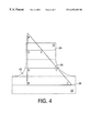
- FIG. 4 illustrates a geometric technique for approximating the effective CTE at the neutral plane of the encapsulant within a flip chip package.
- FIG. 5 illustrates an embodiment of the present invention that relocates the neutral plane of a substrate.
- FIG. 6 is a cross section of an example substrate in current practice.
- FIG. 7 illustrates an embodiment of the present invention for controlling the stiffness of a substrate.
- FIGS. 8A and 8B illustrate the current practice of locating solder balls on the bottom of a substrate.
- FIGS. 9A and 9B illustrate an embodiment of the present invention that uses additional solder balls on the bottom of a substrate.
- FIG. 10 illustrates an embodiment of the present invention that matches the z-direction CTE of the encapsulant with the z-direction CTE of the IC solder joint.
- the present invention discloses methods and apparatuses that improve the reliability of a flip chip plastic ball grid array package that uses underfill encapsulation to help couple an integrated circuit chip to the plastic ball grid array laminate.
- This disclosure describes numerous specific details that includes specific materials, structures, and processes in order to provide a thorough understanding of the present invention.
- this disclosure describes the present invention in terms of a flip chip packaging technique.
- One skilled in the art will appreciate that one may practice the present invention without these specific details.
- this disclosure does not describe some well known processes, specific materials, and semiconductor structures in detail in order not to obscure the present invention.
- FIG. 1 illustrates a typical flip chip PBGA assembly 9 that comprises a semiconductor device or an integrated circuit (IC) chip 10 coupled to a PBGA substrate or laminate 20 through the IC solder joints or bumps 18 .
- An encapsulant 16 couples the IC chip 10 to the laminate 20 .
- the flip chip process “flips” the IC chip upside down so that the device side or face side of the IC chip is the side coupled to the PBGA laminate.
- the bottom of the IC chip 12 is the device side of the IC chip and the top of the IC chip 14 is the back side of the IC chip.
- the flip chip typically has bumps for soldering (IC solder joints) 18 manufactured on the I/O pads of the IC device.
- the IC solder joints take the place of the bonding wires used in non-flip chip packaging.
- the PBGA laminate 20 couples to the printed wiring board (PWB) 11 through the PBGA solder joints 22 .
- the plated through holes (PTH) 13 connect the signals from the IC chip 10 through the laminate 20 on to PWB 11 .
- the electrical signal path is from IC chip 10 through IC solder joints 18 through substrate 20 by way of the PTHs 13 . From the PTHs, the signals go through the PBGA solder joints 22 to PWB 11 .
- FIG. 2 illustrates common reliability problems associated with the flip chip packaging technique.
- Delamination 100 is a separation of layers and it can occur at various interfaces including the interface between the IC chip 10 and IC solder joints 18 , the IC solder joints 18 and the substrate 20 , the substrate 20 and the PBGA solder joints 22 , and the PBGA solder joints 22 and the PWB 11 .
- Warpage 102 is an out of plane displacement and is a manifestation of the mismatches of the coefficient of thermal expansion (CTE) of the IC chip and the CTE of the PBGA laminate.
- CTE coefficient of thermal expansion
- the PBGA laminate 20 shrinks more than the IC chip 10 and causes the back side 14 of the IC chip to be higher in the center (bulge up) and lower at the corners.
- chip cracking 104 may occur because of excessive stresses placed on the IC chip 10 such as from warpage.
- the warpage in the assembled flip chip package causes compression stress on the device side 12 of the IC chip 10 and tensile stress on the back side 14 of the IC chip.
- warpage can also cause solder strain 106 to occur because of the tensile or compression forces placed on the solder joints such as the IC joints 18 .
- FIG. 3 illustrates the current practice for locating the neutral planes within a flip chip package assembly.
- a flip chip package assembly 9 IC chip, encapsulant, and PBGA substrate
- Warpage 102 of FIG. 2
- the substrate 20 shrinks more than the IC chip 10 and causes the back side of the IC chip 10 to be higher in the center (bulge up) and lower at the corners.
- the warpage in the assembled flip chip package causes compression stress on the device side 12 and tensile stress on the back side 14 of the IC chip 10 .
- An excessive tensile stress may cause the IC chip to crack, and an excessive stress on the flip chip package assembly 9 may cause interfacial delamination between the IC chip 10 and the encapsulant 16 and or between the encapsulant 16 and the substrate 20 .
- a typical IC chip 10 has a neutral plane 24 at the middle of the chip thickness (its mid-plane).
- a neutral plane is the plane within a structure where the stress is neutral, while the mid-plane of a structure is the plane that is half way between the top and the bottom of the structure.
- a typical PBGA laminate or substrate 20 has a neutral plane 26 at the middle of the laminate (or its mid-plane).
- CTE coefficient of thermal expansion
- the neutral plane 26 of the laminate 20 will shrink at a CTE of 17 ppm per degree Centigrade.
- the neutral plane 28 of the encapsulant 16 will shrink at an “equivalent” CTE that is somewhere between 3 and 17 ppm per degree Centigrade.
- FIG. 4 illustrates a geometric estimation for approximating the effective CTE at the neutral plane of the encapsulant within a flip chip package assembly.
- the modulus of the encapsulant is much smaller than those of the IC chip 10 and the PBGA laminate 20 , and that the tensile and shear moduli of the IC chip and the laminate substrate are the same.
- the CTE of the laminate 20 (and it's neutral plane 26 ) is 17 ppm per degree Centigrade, and CTE of the IC chip 10 (and it's neutral plane 24 ) is 3 ppm per degree Centigrade.
- the line segment DE corresponds to the CTE of the IC chip's neutral plane 24 .
- the line segment BC corresponds to the laminate's neutral plane 26 .
- the mid-plane 28 of the encapsulant 16 corresponds to the line segment XY.
- FIG. 5 illustrates an embodiment of the present invention that relocates the neutral plane of a substrate. Relocating the neutral plane of the substrate will reduce the compression strain on the device side of the IC chip and reduce the tensile strain on the back side of the IC chip that occur when the encapsulated flip chip package cools from its wiring board assembly temperature to room temperature.
- the following example illustrates the reduced stresses produced by the present invention: if the distance of the IC chip's neutral plane 24 (DE of FIG. 4) is 8 mils from the mid-plane 28 of the encapsulant and the laminate's neutral plane 26 (BC of FIG. 4) is 20 mils from the mid-plane 28 of the encapsulant, using the geometrical model illustrated in FIG. 4 yields:
- the “equivalent” CTE at the interface between the IC chip 10 and the encapsulant 16 will be between 3 and 7, and probably around 6.5 ppm per degree Centigrade.
- This “equivalent” is 3.5 ppm greater than the 3 ppm for the IC chip, instead of 6 ppm greater when the two neutral planes were at an equal distance from the mid-plane 28 of the encapsulant. This represents a 42% reduction in the compression strain on the device side of the IC chip.
- the preferred embodiment of the present invention for relocating the neutral planes has the location of the neutral plane of the substrate moved during the fabrication of the laminate.
- One such technique for relocating the neutral plane is by controlling the stiffness of the PBGA substrate, as described below.
- Another embodiment of the p resent invention that improves the reliability of a flip chip assembly is the control or alteration of t he stiffness of the individual layers within a PBGA laminate.
- the typical practice in manufacturing the separate layers of a PBGA substrate is to make each layer with the same relative stiffness as the other similar layers.
- T hat is each dielectric layer has the same relative stiffness as the other dielectric layers, and each metal layer has the same relative stiffness as the other met al layers.
- the glass transition temperature and the Young's modulus of these layers may be different from each other, but the coefficient of thermal expansion (CTE) for each layer needs to be relatively the same as each other layer, especially for the metal layers in the laminate.
- CTE coefficient of thermal expansion
- an example PBGA substrate or laminate 49 illustrates the current practice for manufacturing the laminate, which comprises the dielectric layers 40 , 42 , and 44 and interspersed between the dielectric layers are the metal layers 46 , 48 , 50 , and 52 .
- the metal layers further comprise a signal layer 46 , a voltage layer 48 , a ground layer 50 , and a signal layer 52 .
- the dielectric layers 40 , 42 , and 44 all have the same relative stiffness to each other, the metal signal layers 46 and 52 have the same relative stiffness to each other (these layers typically comprise a surface area of 10% to 30% metal such as copper), and the metal voltage and ground layers 48 and 50 have the same relative stiffness to each other (these layers typically comprise a surface area of 75% to 85% metal).
- the means that the overall stiffness of the substrate 49 is basically symmetrical from top to bottom.
- the typical laminate 49 further comprises the plated through holes (PTH) 54 , 56 , and 58 for conducting signals from an IC chip through the laminate 49 to a printed wiring board (see for example FIG. 1 ).
- An individual PTH may be formed by a mechanical drilling process or by a laser drilling process for example. After formation of the hole for the PTH, the holes are plated with metal layers 55 , 57 , and 59 for conducting the signals.
- PTH 54 is an example of a plated through hole coupled to the ground layer 50 .
- PTH 56 is an example of a plated through hole coupled to the voltage layer 48 .
- PTH 58 is an example of a plated through hole conducting a signal from the signal layer 46 to the signal layer 52 .
- the metal plated layer of the PTH contacts the metal layer.
- PTH 56 its metal plated layer 57 couples to the voltage layer 48 at point 64 .
- the outer diameter 62 of PTH 56 (including the metal plated layer) is about 14 mils (thousandths of an inch) (where the inner diameter of the interior of PTH is typically 12 mils).
- the diameter of the clearance hole 61 through the metal layer 48 is about 20 mils, which leaves a gap 60 of about 3 mils between the metal layer 48 and the metal plated layer 55 of PTH 54 .
- This embodiment of the present invention improves the reliability of the flip chip package by controlling or varying the stiffness of the PBGA laminate by arranging the metal layers of the laminate accordingly so that the stiffest layer is towards the bottom of the laminate and the least stiff layer is towards the top of the laminate.
- the preferred embodiment of the present invention varies the stiffness of the voltage and ground layers (or the inner layers). For example with reference to FIG. 7, the relative stiffness of the layers would increase from the upper layer of the laminate comprising a metal layer 48 being stiff and a metal layer 50 being stiffer.
- the top layer of the laminate (the layer that contacts the encapsulant), which could be a solder mask, should have a glass transition temperature near that of the encapsulant.
- Controlling or varying the stiffness of the laminate is one technique to relocate the neutral plane of the laminate away from its mid-plane. As previously discussed, relocating the laminate's neutral plane away from the encapsulant allows one to reduce the CTE of the neutral plane of the encapsulant.
- the diameter 82 of the clearance hole around PTH 58 is about 20 mils (similar to the size of the prior method of making the clearance holes as illustrated by FIG. 6 ).
- the stiffness of layer 50 has not changed, although it is now greater than the stiffness of layer 48 due to the changes in layer 48 .
- the stiffness of metal layer 48 it is now less stiff than metal layer 50 .
- the order of relative stiffness of the metal layers is that metal layer 48 is stiff and metal layer 50 is stiffer.
- Another embodiment of the present invention that improves the reliability of a flip chip assembly helps reduce the stresses on the solder joint connections between a PBGA laminate and a PWB (Printed Wiring Board). Additionally, this embodiment helps reduce the bending or warpage of the IC chip. Bending or warpage of the IC chip may prevent the use or placement of a heatsink coupled to the top side of IC chip. Thermal performance of an IC chip is especially important when using high power IC chips that require a high capacity heat sink.
- FIGS. 8A and 8B illustrate the current practice of locating solder joint connections on the bottom of a PBGA substrate for coupling the PBGA substrate to a PWB.
- FIG. 8A is a bottom view of the PBGA substrate 20 .
- the substrate 20 typically has two distinct regions, the first region 32 is underneath the shadow of an IC chip 10 , and the second region 30 is outside the IC chip shadow.
- the “shadow” of the IC chip comprises the area underneath the chip in other structures like the laminate.
- FIG. 8B is a cross section of the flip chip package that illustrates the typical practice of locating the solder joint connections 31 between the PBGA substrate 20 and the PWB 11 , which is to locate the solder balls 31 in the region outside of the chip shadow 30 .
- the IC chip With current flip chip packaging techniques, there is a tendency for the IC chip to bulge up or warp as previously discussed. This tendency for warpage places a mixture of shear stresses and bending stresses on the solder ball interconnections 31 .
- FIGS. 9A and 9B illustrate an embodiment of the present invention that reduces warpage or the bulging of the IC chip by using sacrificial or redundant solder joint connections by locating them in the shadow region of the IC chip.
- FIG. 9A is a bottom view of the PBGA substrate 22 with the shadow region 32 of the IC chip and the region 30 outside of the shadow of the IC chip.
- the solder joint connections 31 carry the signals including power and ground from the PWB through the PBGA laminate to the IC chip.
- This embodiment of the present invention uses additional or redundant voltage and ground solder joint connections 33 located within the shadow region 32 of the IC chip.
- FIG. 9B is a cross section view of FIG. 9A that better illustrates the shadow region 32 and region 30 outside of the shadow region as used in this embodiment of the present invention.
- the use of the additional solder ball connections 33 allows the mixture of shear stresses and bending stresses, which result from the bonding and encapsulation of the IC chip 10 to the laminate 20 , to be spread over a larger number of solder joint connections (that now includes 31 and 33 ) to the PWB 11 .
- the additional solder joint connections as a whole help reduce the shear and bending stress on each individual solder joint connection.
- Some of these “sacrificial” solder joint connections near the center of the shadow region 32 may eventually break, shear, or crack. This is not a concern, however, since the solder joint connections 32 within the shadow region are best utilized for “redundant” interconnections for voltage and ground between the PWB and the IC chip.
- Another embodiment of the present invention that improves the reliability of a flip chip assembly helps reduce the z-direction tensile or compression stresses on the IC solder joint and the encapsulant, which minimizes the risk of the solder joints from lifting away from the chip or the delamination of the encapsulant from the chip or the PBGA laminate.
- This embodiment of the present invention will improve the reliability of the flip chip, for example, when changing the composition of the materials used in the solder joint or the encapsulant or when relocating the neutral planes as described above.
- FIG. 10 illustrates an embodiment of the present invention, which comprises an IC chip 10 coupled to a PBGA substrate 20 with the IC solder joints 18 and an encapsulant 16 .
- IC chip 10 coupled to a PBGA substrate 20 with the IC solder joints 18 and an encapsulant 16 .
- encapsulant 16 we can determine the volumetric CTE by the following equation:
- the CTE of the IC chip 10 is approximately 3 ppm per degree Centigrade and the CTE of the PBGA substrate 20 is approximately 17 ppm per degree Centigrade.
- the “equivalent” CTE of the encapsulant needs to be approximately 10 ppm per degree Centigrade in both the x-direction and the y-direction. If we use a high lead solder for the solder joints 18 with a CTE of 28 ppm per degree Centigrade in the z-direction, then we need to choose an encapsulant with a matching z-direction CTE, which in this example is approximately 28 ppm per degree Centigrade. Using equation (2), the encapsulant used in this flip chip assembly would have a volumetric CTE of 48 ppm per degree Centigrade.
- Equation (2) a constraint or reduction of the x-direction and y-direction of the encapsulant causes changes in the overall volumetric CTE of the encapsulant and also the z-direction CTE of the encapsulant. If the chemical composition of the encapsulant remains unchanged, the volumetric CTE of the encapsulant will still be 48 ppm per degree Centigrade.
- the z-direction CTE of the encapsulant will now be 34 ppm per degree Centigrade, which is much larger than the 28 ppm per degree Centigrade CTE of the solder joint. Therefore, we need to change the composition of the encapsulant (e.g., adjusting the epoxy to ceramic ratio) to have a volumetric CTE of 42 ppm per degree Centigrade, or 28 ppm in the z-direction. If we use the same material in the solder joint as above, then the z-direction CTE of the encapsulant and the solder joint will now match. Additionally, if we change the solder joint material to one with a different z-direction CTE, then we would need to rematch it with the z-direction of the encapsulant.
- the z-direction CTE of the encapsulant including the volumetric CTE is substantially different from z-direction CTE of the solder joint, there will be z-direction tensile or compression stress on the solder joints and the encapsulant.
- a solder joint 18 is under z-direction tensile stress, there will be a separation force on the interface between the IC chip 10 and the under-bump-metallurgy (UBM).
- UBM under-bump-metallurgy
- the encapsulant 16 is under z-direction tensile stress, there will be a separation force on the encapsulant-chip as well as the encapsulant-PBGA laminate interfaces.
- the volumetric CTE of the encapsulant when the volumetric CTE of the encapsulant is much lower than the z-direction CTE of the solder joints, the solder joints encounter tensile stress during the cool down step (of the process for coupling the flip chip assembly), and the encapsulant encounters tensile stress during the heat-up step (of the process for coupling the flip chip assembly).
- the reverse is true when the volumetric CTE of the encapsulant is much higher than the z-direction CTE of the solder joints.
- the bending of the FC PBGA composite structure leads to the reduction of the shear strain in the solder ball interconnections.
- an excessive bending should be avoided to reduce chip stress and to maintain good thermal conduction path to the heat sink. This may involve the tradeoff between solder strain risk and package stress and chip stress and warpage risks.
- the present invention is a collection of techniques that overcome the above disadvantages and improve the overall reliability of the flip chip packaging technique.
- the present invention reduces the probability of an IC chip crack due to excessive stresses such as from warpage. Additionally, the present invention reduces the probability of an interfacial delamination between the IC chip and the encapsulant and or between the encapsulant and the substrate. And, the present invention also improves the reliability of the flip chip packaging technique in its daily uses (as part of a product) under repetitive thermal cycles of normal use.
- the present invention discloses one embodiment that relocates the neutral planes in the PBGA laminate. This embodiment of the present invention reduces the compression strain on the device side of the IC chip and reduces the tensile strain on the back side of the IC chip that occurs when the encapsulated flip chip package assembly cools from its wiring board assembly temperature to room temperature.
- Another embodiment of the present invention controls the stiffness of individual metal layers within the PBGA laminate with a reduction of stiffness from the bottom side to the top side of the laminate. This embodiment reduces warpage and the shear strain on the IC chip solder joints.
- Another embodiment of the present invention uses redundant solder joint connections between the flip chip package and the printed wiring board. These additional solder joint connections help reduce the bending of the IC chip and help improve the placement of any heat sink on the back side of the IC chip. Reducing the bending of the IC chip also helps improve its thermal performance with a heatsink.
- Another embodiment of the present invention matches the z-direction CTE of the IC solder joint with the z-direction CTE of the encapsulant. Consideration of the z-direction CTE's is important when determining the volumetric CTE of the encapsulant.
Abstract
Description
Claims (10)
Priority Applications (1)
| Application Number | Priority Date | Filing Date | Title |
|---|---|---|---|
| US09/050,765 US6353182B1 (en) | 1997-08-18 | 1998-03-30 | Proper choice of the encapsulant volumetric CTE for different PGBA substrates |
Applications Claiming Priority (2)
| Application Number | Priority Date | Filing Date | Title |
|---|---|---|---|
| US08/912,451 US6255599B1 (en) | 1997-08-18 | 1997-08-18 | Relocating the neutral plane in a PBGA substrate to eliminate chip crack and interfacial delamination |
| US09/050,765 US6353182B1 (en) | 1997-08-18 | 1998-03-30 | Proper choice of the encapsulant volumetric CTE for different PGBA substrates |
Related Parent Applications (1)
| Application Number | Title | Priority Date | Filing Date |
|---|---|---|---|
| US08/912,451 Continuation-In-Part US6255599B1 (en) | 1997-08-18 | 1997-08-18 | Relocating the neutral plane in a PBGA substrate to eliminate chip crack and interfacial delamination |
Publications (1)
| Publication Number | Publication Date |
|---|---|
| US6353182B1 true US6353182B1 (en) | 2002-03-05 |
Family
ID=46276226
Family Applications (1)
| Application Number | Title | Priority Date | Filing Date |
|---|---|---|---|
| US09/050,765 Expired - Fee Related US6353182B1 (en) | 1997-08-18 | 1998-03-30 | Proper choice of the encapsulant volumetric CTE for different PGBA substrates |
Country Status (1)
| Country | Link |
|---|---|
| US (1) | US6353182B1 (en) |
Cited By (7)
| Publication number | Priority date | Publication date | Assignee | Title |
|---|---|---|---|---|
| US6661102B1 (en) * | 2002-01-18 | 2003-12-09 | Advance Micro Devices, Inc. | Semiconductor packaging apparatus for controlling die attach fillet height to reduce die shear stress |
| US6888230B1 (en) * | 1998-10-28 | 2005-05-03 | Renesas Technology Corp. | Semiconductor device, semiconductor wafer, semiconductor module, and a method of manufacturing semiconductor device |
| US20050275094A1 (en) * | 2001-09-27 | 2005-12-15 | Intel Corporation. | Encapsulation of pin solder for maintaining accuracy in pin position |
| US6977338B1 (en) * | 2004-07-28 | 2005-12-20 | Kabushiki Kaisha Toshiba | Wiring board and magnetic disk apparatus |
| US6995476B2 (en) * | 1998-07-01 | 2006-02-07 | Seiko Epson Corporation | Semiconductor device, circuit board and electronic instrument that include an adhesive with conductive particles therein |
| US20070206455A1 (en) * | 2006-03-06 | 2007-09-06 | Masanori Minamio | Optical device and method for manufacturing the same |
| CN100437990C (en) * | 2005-03-17 | 2008-11-26 | 台湾积体电路制造股份有限公司 | Strain silicon wafer with a crystal orientation (100) in flip chip bga package |
Citations (13)
| Publication number | Priority date | Publication date | Assignee | Title |
|---|---|---|---|---|
| US4849284A (en) * | 1987-02-17 | 1989-07-18 | Rogers Corporation | Electrical substrate material |
| US4888061A (en) * | 1988-09-01 | 1989-12-19 | Minnesota Mining And Manufacturing Company | Thin-film solar cells resistant to damage during flexion |
| US5089440A (en) * | 1990-03-14 | 1992-02-18 | International Business Machines Corporation | Solder interconnection structure and process for making |
| US5121190A (en) * | 1990-03-14 | 1992-06-09 | International Business Machines Corp. | Solder interconnection structure on organic substrates |
| US5194930A (en) * | 1991-09-16 | 1993-03-16 | International Business Machines | Dielectric composition and solder interconnection structure for its use |
| US5274913A (en) * | 1991-10-25 | 1994-01-04 | International Business Machines Corporation | Method of fabricating a reworkable module |
| US5450283A (en) * | 1992-11-03 | 1995-09-12 | Motorola, Inc. | Thermally enhanced semiconductor device having exposed backside and method for making the same |
| US5463191A (en) * | 1994-03-14 | 1995-10-31 | Dell Usa, L.P. | Circuit board having an improved fine pitch ball grid array and method of assembly therefor |
| US5553769A (en) * | 1992-11-12 | 1996-09-10 | International Business Machine Corporation | Interconnection of a carrier substrate and a semiconductor device |
| US5583377A (en) * | 1992-07-15 | 1996-12-10 | Motorola, Inc. | Pad array semiconductor device having a heat sink with die receiving cavity |
| US5627407A (en) * | 1995-04-28 | 1997-05-06 | Lucent Technologies Inc. | Electronic package with reduced bending stress |
| US5796590A (en) * | 1996-11-05 | 1998-08-18 | Micron Electronics, Inc. | Assembly aid for mounting packaged integrated circuit devices to printed circuit boards |
| US5928404A (en) * | 1997-03-28 | 1999-07-27 | Ford Motor Company | Electrical solder and method of manufacturing |
-
1998
- 1998-03-30 US US09/050,765 patent/US6353182B1/en not_active Expired - Fee Related
Patent Citations (14)
| Publication number | Priority date | Publication date | Assignee | Title |
|---|---|---|---|---|
| US4849284A (en) * | 1987-02-17 | 1989-07-18 | Rogers Corporation | Electrical substrate material |
| US4888061A (en) * | 1988-09-01 | 1989-12-19 | Minnesota Mining And Manufacturing Company | Thin-film solar cells resistant to damage during flexion |
| US5089440A (en) * | 1990-03-14 | 1992-02-18 | International Business Machines Corporation | Solder interconnection structure and process for making |
| US5121190A (en) * | 1990-03-14 | 1992-06-09 | International Business Machines Corp. | Solder interconnection structure on organic substrates |
| US5194930A (en) * | 1991-09-16 | 1993-03-16 | International Business Machines | Dielectric composition and solder interconnection structure for its use |
| US5274913A (en) * | 1991-10-25 | 1994-01-04 | International Business Machines Corporation | Method of fabricating a reworkable module |
| US5583377A (en) * | 1992-07-15 | 1996-12-10 | Motorola, Inc. | Pad array semiconductor device having a heat sink with die receiving cavity |
| US5450283A (en) * | 1992-11-03 | 1995-09-12 | Motorola, Inc. | Thermally enhanced semiconductor device having exposed backside and method for making the same |
| US5553769A (en) * | 1992-11-12 | 1996-09-10 | International Business Machine Corporation | Interconnection of a carrier substrate and a semiconductor device |
| US5920125A (en) * | 1992-11-12 | 1999-07-06 | International Business Machines Corporation | Interconnection of a carrier substrate and a semiconductor device |
| US5463191A (en) * | 1994-03-14 | 1995-10-31 | Dell Usa, L.P. | Circuit board having an improved fine pitch ball grid array and method of assembly therefor |
| US5627407A (en) * | 1995-04-28 | 1997-05-06 | Lucent Technologies Inc. | Electronic package with reduced bending stress |
| US5796590A (en) * | 1996-11-05 | 1998-08-18 | Micron Electronics, Inc. | Assembly aid for mounting packaged integrated circuit devices to printed circuit boards |
| US5928404A (en) * | 1997-03-28 | 1999-07-27 | Ford Motor Company | Electrical solder and method of manufacturing |
Non-Patent Citations (4)
| Title |
|---|
| Powell, Trivedi, "Flip-Chip on FR-4 Integrated Circuit Packaging," 1993 Electronic Components and Technology Conference, IEEE, pp. 182-186. |
| Serway Raymond A., Physics For Scientist & Engineers, Textbook, pp. 514,and 515, 1992.* |
| Tsukada, Tsuchida, Mashimoto, "Surface Laminar Circuit Packaging," Yasu Technology Application Laboratory, IBM Japan, IEEE, 1992, pp. 22-27. |
| Wu, Tsukada, Chen, "Materials and Mechanics Issues in Flip-Chip Organic Packaging," 1996 Electronic Components and Technology Conference, IEEE, pp. 524-534. |
Cited By (14)
| Publication number | Priority date | Publication date | Assignee | Title |
|---|---|---|---|---|
| US20070132099A1 (en) * | 1998-07-01 | 2007-06-14 | Seiko Epson Corporation | Semiconductor device and method of manufacture thereof, circuit board and electronic instrument |
| US7198984B2 (en) | 1998-07-01 | 2007-04-03 | Seiko Epson Corporation | Semiconductor device and method of manufacture thereof, circuit board and electronic instrument |
| US7560819B2 (en) | 1998-07-01 | 2009-07-14 | Seiko Epson Corporation | Semiconductor device and method of manufacture thereof, circuit board and electronic instrument |
| US20060099739A1 (en) * | 1998-07-01 | 2006-05-11 | Seiko Epson Corporation | Semiconductor device and method of manufacture thereof, circuit board and electronic instrument |
| US6995476B2 (en) * | 1998-07-01 | 2006-02-07 | Seiko Epson Corporation | Semiconductor device, circuit board and electronic instrument that include an adhesive with conductive particles therein |
| US6888230B1 (en) * | 1998-10-28 | 2005-05-03 | Renesas Technology Corp. | Semiconductor device, semiconductor wafer, semiconductor module, and a method of manufacturing semiconductor device |
| US7217992B2 (en) | 1998-10-28 | 2007-05-15 | Renesas Technology Corp. | Semiconductor device, semiconductor wafer, semiconductor module, and a method of manufacturing semiconductor device |
| US7211888B2 (en) * | 2001-09-27 | 2007-05-01 | Intel Corporation | Encapsulation of pin solder for maintaining accuracy in pin position |
| US20050275094A1 (en) * | 2001-09-27 | 2005-12-15 | Intel Corporation. | Encapsulation of pin solder for maintaining accuracy in pin position |
| US6661102B1 (en) * | 2002-01-18 | 2003-12-09 | Advance Micro Devices, Inc. | Semiconductor packaging apparatus for controlling die attach fillet height to reduce die shear stress |
| US6977338B1 (en) * | 2004-07-28 | 2005-12-20 | Kabushiki Kaisha Toshiba | Wiring board and magnetic disk apparatus |
| CN100437990C (en) * | 2005-03-17 | 2008-11-26 | 台湾积体电路制造股份有限公司 | Strain silicon wafer with a crystal orientation (100) in flip chip bga package |
| US20070206455A1 (en) * | 2006-03-06 | 2007-09-06 | Masanori Minamio | Optical device and method for manufacturing the same |
| US20110083322A1 (en) * | 2006-03-06 | 2011-04-14 | Panasonic Corporation | Optical device and method for manufacturing the same |
Similar Documents
| Publication | Publication Date | Title |
|---|---|---|
| US5616520A (en) | Semiconductor integrated circuit device and fabrication method thereof | |
| US6255143B1 (en) | Flip chip thermally enhanced ball grid array | |
| US5959348A (en) | Construction of PBGA substrate for flip chip packing | |
| US9373573B2 (en) | Solder joint flip chip interconnection | |
| US7517778B2 (en) | Structure of high performance combo chip and processing method | |
| KR100480515B1 (en) | Semiconductor device | |
| KR100276054B1 (en) | Organic controlled collapse chip connector (c4) ball grid array (bga) chip carrier with dual thermal expansion rates | |
| US6297141B1 (en) | Mounting assembly of integrated circuit device and method for production thereof | |
| EP0908952A2 (en) | Chip-on-chip IC packages | |
| US6829149B1 (en) | Placement of sacrificial solder balls underneath the PBGA substrate | |
| US20050056943A1 (en) | Integrated electronic chip and interconnect device and process for making the same | |
| US8361598B2 (en) | Substrate anchor structure and method | |
| US6664621B2 (en) | Semiconductor chip package with interconnect structure | |
| JPS63177434A (en) | Electronic component connecting structure and manufacture thereof | |
| USRE44562E1 (en) | Solder joint flip chip interconnection having relief structure | |
| JPH05211202A (en) | Composite flip-chip semiconductor device, its manufacture and method for burn-in | |
| USRE44608E1 (en) | Solder joint flip chip interconnection | |
| US7038309B2 (en) | Chip package structure with glass substrate | |
| US20110037179A1 (en) | Semiconductor package | |
| US6353182B1 (en) | Proper choice of the encapsulant volumetric CTE for different PGBA substrates | |
| US6255599B1 (en) | Relocating the neutral plane in a PBGA substrate to eliminate chip crack and interfacial delamination | |
| CN1257545C (en) | Method for mfg. electronic packaging, and electronic package | |
| US6407927B1 (en) | Method and structure to increase reliability of input/output connections in electrical devices | |
| JPH06333982A (en) | Manufacture of semiconductor integrated circuit device | |
| US6632690B2 (en) | Method of fabricating reliable laminate flip-chip assembly |
Legal Events
| Date | Code | Title | Description |
|---|---|---|---|
| AS | Assignment |
Owner name: INTERNATIONAL BUSINESS MACHINES CORPORATION, NEW Y Free format text: ASSIGNMENT OF ASSIGNORS INTEREST;ASSIGNOR:CHEN, WILLIAM T.;REEL/FRAME:009412/0230 Effective date: 19980619 |
|
| AS | Assignment |
Owner name: SEMATECH, INC., TEXAS Free format text: ASSIGNMENT OF ASSIGNORS INTEREST;ASSIGNOR:CHANG, CHI-SHIH;REEL/FRAME:009412/0800 Effective date: 19980820 Owner name: INTERNATIONAL BUSINESS MACHINES CORPORATION, NEW Y Free format text: ASSIGNMENT OF ASSIGNORS INTEREST;ASSIGNOR:TRIVEDI, AJIT;REEL/FRAME:009412/0235 Effective date: 19980608 |
|
| FPAY | Fee payment |
Year of fee payment: 4 |
|
| FEPP | Fee payment procedure |
Free format text: PAYOR NUMBER ASSIGNED (ORIGINAL EVENT CODE: ASPN); ENTITY STATUS OF PATENT OWNER: LARGE ENTITY |
|
| FPAY | Fee payment |
Year of fee payment: 8 |
|
| REMI | Maintenance fee reminder mailed | ||
| LAPS | Lapse for failure to pay maintenance fees | ||
| STCH | Information on status: patent discontinuation |
Free format text: PATENT EXPIRED DUE TO NONPAYMENT OF MAINTENANCE FEES UNDER 37 CFR 1.362 |
|
| FP | Lapsed due to failure to pay maintenance fee |
Effective date: 20140305 |