US6342778B1 - Low profile, surface mount magnetic devices - Google Patents
Low profile, surface mount magnetic devices Download PDFInfo
- Publication number
- US6342778B1 US6342778B1 US09/552,811 US55281100A US6342778B1 US 6342778 B1 US6342778 B1 US 6342778B1 US 55281100 A US55281100 A US 55281100A US 6342778 B1 US6342778 B1 US 6342778B1
- Authority
- US
- United States
- Prior art keywords
- magnetic
- magnetic core
- conductors
- conductive elements
- power supply
- Prior art date
- Legal status (The legal status is an assumption and is not a legal conclusion. Google has not performed a legal analysis and makes no representation as to the accuracy of the status listed.)
- Expired - Lifetime
Links
- 230000005291 magnetic effect Effects 0.000 title claims abstract description 102
- 239000004020 conductor Substances 0.000 claims description 29
- 238000004519 manufacturing process Methods 0.000 claims description 8
- 230000001105 regulatory effect Effects 0.000 claims description 3
- 239000004065 semiconductor Substances 0.000 claims 1
- 238000005452 bending Methods 0.000 description 5
- 239000000758 substrate Substances 0.000 description 5
- 238000000034 method Methods 0.000 description 4
- 238000004804 winding Methods 0.000 description 4
- 239000000463 material Substances 0.000 description 3
- XEEYBQQBJWHFJM-UHFFFAOYSA-N Iron Chemical compound [Fe] XEEYBQQBJWHFJM-UHFFFAOYSA-N 0.000 description 2
- 230000015572 biosynthetic process Effects 0.000 description 2
- 230000004907 flux Effects 0.000 description 2
- 229910000859 α-Fe Inorganic materials 0.000 description 2
- RYGMFSIKBFXOCR-UHFFFAOYSA-N Copper Chemical compound [Cu] RYGMFSIKBFXOCR-UHFFFAOYSA-N 0.000 description 1
- 230000004075 alteration Effects 0.000 description 1
- 239000003990 capacitor Substances 0.000 description 1
- 238000010276 construction Methods 0.000 description 1
- 229910052802 copper Inorganic materials 0.000 description 1
- 239000010949 copper Substances 0.000 description 1
- 230000007812 deficiency Effects 0.000 description 1
- 238000010586 diagram Methods 0.000 description 1
- 239000003989 dielectric material Substances 0.000 description 1
- 238000007689 inspection Methods 0.000 description 1
- 229910052742 iron Inorganic materials 0.000 description 1
- 239000000696 magnetic material Substances 0.000 description 1
- 238000006467 substitution reaction Methods 0.000 description 1
Images


Classifications
-
- H—ELECTRICITY
- H01—ELECTRIC ELEMENTS
- H01F—MAGNETS; INDUCTANCES; TRANSFORMERS; SELECTION OF MATERIALS FOR THEIR MAGNETIC PROPERTIES
- H01F17/00—Fixed inductances of the signal type
- H01F17/0006—Printed inductances
- H01F17/0033—Printed inductances with the coil helically wound around a magnetic core
-
- H—ELECTRICITY
- H01—ELECTRIC ELEMENTS
- H01F—MAGNETS; INDUCTANCES; TRANSFORMERS; SELECTION OF MATERIALS FOR THEIR MAGNETIC PROPERTIES
- H01F17/00—Fixed inductances of the signal type
- H01F17/04—Fixed inductances of the signal type with magnetic core
- H01F17/045—Fixed inductances of the signal type with magnetic core with core of cylindric geometry and coil wound along its longitudinal axis, i.e. rod or drum core
Definitions
- the invention relates to magnetic devices such as inductors and transformers. Specifically, the invention relates to magnetic devices that can be assembled as low profile surface mount devices on a printed circuit board or a metallized substrate.
- Magnetic devices such as inductors and transformers, are employed in many different types of electrical devices including communications equipment and power supplies.
- most magnetic devices are fabricated of one or more windings, formed by an elongated electrical conductor, such as a wire of circular or rectangular cross-section, or a planar electrical conductor wound about or mounted to a bobbin composed of a dielectric material, such as plastic.
- the electrical member is soldered to terminations on the bobbin.
- the electrical member may be threaded through the bobbin for connection directly to a metallized area of an underlying circuit board.
- a magnetic core may be disposed about the bobbin to impart a greater reactance to the magnetic device and thereby alter its operating characteristics.
- the use of a bobbin generally results in a magnetic device with a large profile, which not only takes up valuable space on the circuit board, but also results in a large height for the overall electrical device.
- magnetic devices can be formed with a magnetic core, such as ferrite or iron, wound with conductive coils. These devices are sometimes referred to as wire-wound core devices.
- wire-wound core devices One major difficulty with wire-wound core devices is that they have been difficult to miniaturize. While components such as resistors, diodes, capacitors and transistors have been drastically reduced in size, magnetics, including bobbin and wire-wound core devices, remain bulky.
- the device described in Roy et al. is a magnetic component formed by a plurality of conductive elements surrounding a magnetic core.
- the conductive elements pass through holes or channels in the magnetic core and then are bent outwards to allow surface mount connection to a printed wiring board or the equivalent.
- the magnetic component described by Roy et al. suffers from a number of deficiencies.
- the device is incapable of carrying large amounts of current because the small area of the magnetic core that is surrounded by the conductive elements tends to saturate quickly.
- the bent out ends of the conductive elements make poor surface mount conductors because they are very difficult to make coplanar.
- the magnetic components of Roy et al. can be difficult to manufacture due to the shape of the magnetic core and the arrangement of the conductive elements.
- Embodiments of the invention include providing for a low profile magnetic component formed from a magnetic core and a plurality of conductive elements, also referred to as conductors.
- the magnetic core includes a bottom, a top, end surfaces and side surfaces.
- the side surfaces include portions that are angled inward from the bottom to the top thereby forming a plurality of channels.
- the magnetic core further includes a recess in the top adjacent to the channels.
- the plurality of conductors surround the magnetic core and pass through a corresponding channel from the plurality of channels.
- the top of the conductors are adjacent to the recess in the magnetic core and the ends are bent inward against the bottom of the core.
- the ends of the conductors form contact surfaces which are coplanar and surface mountable.
- the tops of the conductors are loaded causing the ends to bend inward in to the recess in the magnetic core. While the conductors are loaded the ends are bent inward toward the center of the bottom. After bending, the conductors are unloaded and the spring tension in the conductors causes them to fit tightly around the magnetic core and causes the ends to fit snugly against the base.
- the magnetic components can be formed into a magnetic device such as an inductor by placing two or more in close proximity and using conductive traces on a printed wiring board or other insulated substrate to form the conductors into windings.
- This magnetic device can then be utilized in a power supply as, for example, the inductor in an output filter or as transformers in groups of two or more.
- FIG. 1 is a perspective view of a low profile magnetic component according to a conventional arrangement
- FIG. 2 a is a perspective view of a low profile magnetic component according to an embodiment of the invention.
- FIG. 2 b is a cross-sectional view of the magnetic component from FIG. 2 a;
- FIG. 3 is plan view of a magnetic device formed from an insulating substrate with conductive traces and two of the magnetic components from FIG. 2;
- FIG. 4 is a circuit diagram showing a power supply incorporating the magnetic device from FIG. 3;
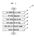
- FIG. 5 is a flow chart describing a process for making a low profile magnetic device in accordance with the principles of the invention.
- Magnetic component 10 is formed by body 11 of magnetic material that is surrounded by a plurality of conductive elements 12 distributed along the major dimension of body 11 .
- Each conductive element 12 is formed with four right angle bends, the first and second bends allowing conductive element 12 to pass through channels 16 to surround a portion of the body, and the third and fourth bends to form a pair of contact surfaces 14 .
- Magnetic component 10 suffers from a variety of drawbacks. First, by having conductive elements 12 pass at right angles through channels 16 , a large portion of the cross-section of body 11 is not surrounded by conductive elements 12 .
- the magnetic flux able to be carried by body 11 is limited.
- the third and fourth bends that form contact surfaces 14 are formed by bending conductive element 12 outward in free space. By forming contact surfaces 14 in this manner making them coplanar for surface mounting within specific tolerances is very difficult.
- magnetic component 10 is manufactured by taking the preformed conductive elements and placing them around body 11 . This type of manufacturing is difficult and only exacerbates the problem of trying to make contact surfaces 14 for all conductive elements 12 coplanar. If one conductive element 12 is misplaced by as little as a few thousands of an inch the coplanarity of the entire device is unacceptable.
- a low-profile magnetic component that a) uses as much of the cross-section of the magnetic core as possible, b) has conductive elements with contact surfaces that are tightly coplanar, and c) is easy to manufacture within design tolerances.
- Low-profile magnetic component 20 shown in FIGS. 2 a and 2 b is formed from magnetic core 22 and a plurality of conductive elements 24 .
- Magnetic core 22 typically is rectangular in shape, having a length l greater than the width w and height h.
- Conductive elements 24 are located in a center section 26 along the length l of magnetic core 22 .
- Center section 26 contains a number of features to accommodate conductive elements 24 , including recess 28 in the top 34 of magnetic core 22 , and channels 30 , which further include angled side surfaces 32 . Angled side surfaces 32 form a cross section that increases from top 34 to some distance above bottom 36 of magnetic core 22 .
- the angled side surfaces allow for better inspection capability of the assembled component. Wrapping the conductive elements 24 around the outside of magnetic core 22 allows more cross-sectional area to be surrounded by conductive elements 24 . This greater crosssectional area increases the amount of flux that can be handled by the core before saturation, and therefore, increases the amount of current that the magnetic device can accommodate.
- Conductive elements 24 are also formed with coplanar contact surfaces 38 .
- contact surfaces 38 are formed by bending conductive elements 24 inward against the bottom 36 of magnetic core 22 . Bending conductive elements 24 inward to form contact surfaces 38 allows for much greater control over the coplanarity of the contact surfaces.
- Bottom 36 of magnetic core 22 is used as a stop to ensure consistent coplanarity both between contact surfaces 38 of a specific conductive element 24 as well as between contact surfaces 38 of different conductive elements 24 .
- Recess 28 in top 34 of magnetic core 22 , aids in the formation of contact surfaces 38 .
- the top of conductive element 24 is displaced into recess 28 before it is bent to form contact surfaces 38 .
- conductive element 24 After contact surfaces 38 are bent into place, the top of conductive element 24 is unloaded releasing the spring tension, which causes contact surfaces 38 to curl tightly up against bottom 36 of magnetic core 22 .
- Use of this loading of conductive element 24 allows a much more consistent formation of contact surfaces 38 which result in very coplanar surface mount contacts.
- the loading technique also allows conductive elements 24 to fit more tightly around magnetic core 22 to limit any potential movement of the conductive elements 24 .
- a magnetic device is formed from magnetic component 22 by mounting two or more devices in close proximity on an insulating substrate having conductive traces for interconnecting the conductive elements of the magnetic component into windings.
- FIG. 3 shows a magnetic device 40 formed from a pair of magnetic components 20 A and 20 B placed side by side to form an air gap 42 between them.
- Conductive trace 41 on an insulating substrate, such as printed wiring board 44 is used to interconnect the conductive elements of magnetic devices 20 A and 20 B into windings.
- the magnetic components 20 A and 20 B, air gap 40 and conductive trace 41 together form a magnetic device 42 such as an inductor.
- magnetic device 40 is formed using two magnetic components, those skilled in the art would understand that similar magnetic devices could be formed using any number of magnetic components.
- the inductor formed by magnetic device 40 from FIG. 3 is suitable as a magnetic element in a power supply module.
- the circuit for such a power supply module 50 is shown in FIG. 4 .
- Power supply module 50 is formed by buck converter 52 with input voltage 54 , power switches 56 , output filter 58 and regulated output voltage 60 .
- Inductor 62 in output filter 58 is formed from magnetic device 40 from FIG. 3 .
- the operation of buck converter 50 is well understood in the art and will not be discussed further.
- the magnetic device is shown with reference to a buck-type converter, those skilled in the art would understand that the magnetic device according to embodiments of the invention is suitable for use in any type power supply which utilizes magnetic devices, particularly inductors.
- Manufacturing process 60 begins at step 62 by cutting conductive elements 24 to the required length from a continuous supply of conductive material. Once the conductors are cut to length, the process proceeds to step 64 where the conductors are preformed by bending them into a u-shape such that they will fit around the magnetic core 22 . Step 66 then requires that the conductors be placed around magnetic core 22 . In step 68 the tops of the conductors are loaded forcing them down slightly into recess 28 as was described with reference to FIGS. 2 a and 2 b .
- step 70 the ends of the conductors are bent inward against the bottom 36 of magnetic core 22 to form contact surfaces 38 .
- the tops of conductors, or conductive elements 24 are unloaded allowing the conductors to fit snugly to the magnetic core 22 and allowing contact surfaces 38 to form coplanar surfaces for surface mounting.
- the embodiment magnetic core 22 is a ferrite material.
- the conductive elements 24 are formed from copper, which is coated for solderability.
Landscapes
- Engineering & Computer Science (AREA)
- Power Engineering (AREA)
- Microelectronics & Electronic Packaging (AREA)
- Coils Or Transformers For Communication (AREA)
Abstract
Description
Claims (5)
Priority Applications (1)
| Application Number | Priority Date | Filing Date | Title |
|---|---|---|---|
| US09/552,811 US6342778B1 (en) | 2000-04-20 | 2000-04-20 | Low profile, surface mount magnetic devices |
Applications Claiming Priority (1)
| Application Number | Priority Date | Filing Date | Title |
|---|---|---|---|
| US09/552,811 US6342778B1 (en) | 2000-04-20 | 2000-04-20 | Low profile, surface mount magnetic devices |
Publications (1)
| Publication Number | Publication Date |
|---|---|
| US6342778B1 true US6342778B1 (en) | 2002-01-29 |
Family
ID=24206902
Family Applications (1)
| Application Number | Title | Priority Date | Filing Date |
|---|---|---|---|
| US09/552,811 Expired - Lifetime US6342778B1 (en) | 2000-04-20 | 2000-04-20 | Low profile, surface mount magnetic devices |
Country Status (1)
| Country | Link |
|---|---|
| US (1) | US6342778B1 (en) |
Cited By (28)
| Publication number | Priority date | Publication date | Assignee | Title |
|---|---|---|---|---|
| US20020067234A1 (en) * | 2000-12-01 | 2002-06-06 | Samuel Kung | Compact surface-mountable inductors |
| US20080001699A1 (en) * | 2006-06-30 | 2008-01-03 | Gardner Donald S | Slotted magnetic material for integrated circuit inductors |
| US20090231081A1 (en) * | 2008-03-14 | 2009-09-17 | Alexandr Ikriannikov | Voltage Converter Inductor Having A Nonlinear Inductance Value |
| US7864016B1 (en) | 2002-12-13 | 2011-01-04 | Volterra Semiconductor Corporation | Method for making magnetic components with N-phase coupling, and related inductor structures |
| US20110018669A1 (en) * | 2009-07-22 | 2011-01-27 | Alexandr Ikriannikov | Low Profile Inductors For High Density Circuit Boards |
| US7893806B1 (en) * | 2002-12-13 | 2011-02-22 | Volterra Semiconductor Corporation | Method for making magnetic components with N-phase coupling, and related inductor structures |
| US20110043317A1 (en) * | 2009-07-22 | 2011-02-24 | Alexandr Ikriannikov | Low Profile Inductors For High Density Circuit Boards |
| US7898379B1 (en) | 2002-12-13 | 2011-03-01 | Volterra Semiconductor Corporation | Method for making magnetic components with N-phase coupling, and related inductor structures |
| US20110148560A1 (en) * | 2009-12-21 | 2011-06-23 | Alexandr Ikriannikov | Two-Phase Coupled Inductors Which Promote Improved Printed Circuit Board Layout |
| US20110148559A1 (en) * | 2009-12-21 | 2011-06-23 | Alexandr Ikriannikov | multi-turn inductors |
| WO2011149520A1 (en) * | 2010-05-26 | 2011-12-01 | Tyco Electronics Corporation | Planar inductor devices |
| US8299885B2 (en) | 2002-12-13 | 2012-10-30 | Volterra Semiconductor Corporation | Method for making magnetic components with M-phase coupling, and related inductor structures |
| US8406007B1 (en) | 2009-12-09 | 2013-03-26 | Universal Lighting Technologies, Inc. | Magnetic circuit board connector component |
| US8416043B2 (en) | 2010-05-24 | 2013-04-09 | Volterra Semiconductor Corporation | Powder core material coupled inductors and associated methods |
| US8638187B2 (en) | 2009-07-22 | 2014-01-28 | Volterra Semiconductor Corporation | Low profile inductors for high density circuit boards |
| US8674802B2 (en) | 2009-12-21 | 2014-03-18 | Volterra Semiconductor Corporation | Multi-turn inductors |
| US20140266558A1 (en) * | 2013-03-15 | 2014-09-18 | General Electric Company | Integrated magnetic assemblies and methods of assembling same |
| US8952776B2 (en) | 2002-12-13 | 2015-02-10 | Volterra Semiconductor Corporation | Powder core material coupled inductors and associated methods |
| US8975995B1 (en) | 2012-08-29 | 2015-03-10 | Volterra Semiconductor Corporation | Coupled inductors with leakage plates, and associated systems and methods |
| US9013259B2 (en) | 2010-05-24 | 2015-04-21 | Volterra Semiconductor Corporation | Powder core material coupled inductors and associated methods |
| US9263177B1 (en) | 2012-03-19 | 2016-02-16 | Volterra Semiconductor LLC | Pin inductors and associated systems and methods |
| US9281739B2 (en) | 2012-08-29 | 2016-03-08 | Volterra Semiconductor LLC | Bridge magnetic devices and associated systems and methods |
| US9373438B1 (en) | 2011-11-22 | 2016-06-21 | Volterra Semiconductor LLC | Coupled inductor arrays and associated methods |
| US9767947B1 (en) | 2011-03-02 | 2017-09-19 | Volterra Semiconductor LLC | Coupled inductors enabling increased switching stage pitch |
| US10128035B2 (en) | 2011-11-22 | 2018-11-13 | Volterra Semiconductor LLC | Coupled inductor arrays and associated methods |
| EP3713027A1 (en) * | 2019-03-20 | 2020-09-23 | ABB Schweiz AG | Bus bar arrangement with magnetic shielding between the conductive bars |
| US10854370B2 (en) | 2014-12-19 | 2020-12-01 | Texas Instruments Incorporated | Embedded coil assembly and method of making |
| US20220132695A1 (en) * | 2020-10-26 | 2022-04-28 | Modular Power Technology, Inc. | Apparatus for power module and heat dissipation of an integrated circuit |
Citations (3)
| Publication number | Priority date | Publication date | Assignee | Title |
|---|---|---|---|---|
| US5574420A (en) | 1994-05-27 | 1996-11-12 | Lucent Technologies Inc. | Low profile surface mounted magnetic devices and components therefor |
| US6094123A (en) * | 1998-09-25 | 2000-07-25 | Lucent Technologies Inc. | Low profile surface mount chip inductor |
| US6118351A (en) * | 1997-06-10 | 2000-09-12 | Lucent Technologies Inc. | Micromagnetic device for power processing applications and method of manufacture therefor |
-
2000
- 2000-04-20 US US09/552,811 patent/US6342778B1/en not_active Expired - Lifetime
Patent Citations (3)
| Publication number | Priority date | Publication date | Assignee | Title |
|---|---|---|---|---|
| US5574420A (en) | 1994-05-27 | 1996-11-12 | Lucent Technologies Inc. | Low profile surface mounted magnetic devices and components therefor |
| US6118351A (en) * | 1997-06-10 | 2000-09-12 | Lucent Technologies Inc. | Micromagnetic device for power processing applications and method of manufacture therefor |
| US6094123A (en) * | 1998-09-25 | 2000-07-25 | Lucent Technologies Inc. | Low profile surface mount chip inductor |
Cited By (58)
| Publication number | Priority date | Publication date | Assignee | Title |
|---|---|---|---|---|
| US20020067234A1 (en) * | 2000-12-01 | 2002-06-06 | Samuel Kung | Compact surface-mountable inductors |
| US9019064B2 (en) | 2002-12-13 | 2015-04-28 | Volterra Semiconductor Corporation | Method for making magnetic components with M-phase coupling, and related inductor structures |
| US9147515B2 (en) | 2002-12-13 | 2015-09-29 | Volterra Semiconductor LLC | Method for making magnetic components with M-phase coupling, and related inductor structures |
| US8350658B1 (en) | 2002-12-13 | 2013-01-08 | Volterra Semiconductor Corporation | Method for making magnetic components with N-phase coupling, and related inductor structures |
| US8299885B2 (en) | 2002-12-13 | 2012-10-30 | Volterra Semiconductor Corporation | Method for making magnetic components with M-phase coupling, and related inductor structures |
| US8952776B2 (en) | 2002-12-13 | 2015-02-10 | Volterra Semiconductor Corporation | Powder core material coupled inductors and associated methods |
| US7864016B1 (en) | 2002-12-13 | 2011-01-04 | Volterra Semiconductor Corporation | Method for making magnetic components with N-phase coupling, and related inductor structures |
| US8836461B2 (en) | 2002-12-13 | 2014-09-16 | Volterra Semiconductor Corporation | Method for making magnetic components with M-phase coupling, and related inductor structures |
| US7893806B1 (en) * | 2002-12-13 | 2011-02-22 | Volterra Semiconductor Corporation | Method for making magnetic components with N-phase coupling, and related inductor structures |
| US8786395B2 (en) | 2002-12-13 | 2014-07-22 | Volterra Semiconductor Corporation | Method for making magnetic components with M-phase coupling, and related inductor structures |
| US7898379B1 (en) | 2002-12-13 | 2011-03-01 | Volterra Semiconductor Corporation | Method for making magnetic components with N-phase coupling, and related inductor structures |
| US8847722B2 (en) | 2002-12-13 | 2014-09-30 | Volterra Semiconductor Corporation | Method for making magnetic components with N-phase coupling, and related inductor structures |
| US8779885B2 (en) | 2002-12-13 | 2014-07-15 | Volterra Semiconductor Corporation | Method for making magnetic components with M-phase coupling, and related inductor structures |
| US20080001699A1 (en) * | 2006-06-30 | 2008-01-03 | Gardner Donald S | Slotted magnetic material for integrated circuit inductors |
| US7518481B2 (en) * | 2006-06-30 | 2009-04-14 | Intel Corporation | Slotted magnetic material for integrated circuit inductors |
| US8108984B2 (en) | 2006-06-30 | 2012-02-07 | Intel Corporation | Method for manufacturing integrated circuit inductors having slotted magnetic material |
| US20090207576A1 (en) * | 2006-06-30 | 2009-08-20 | Intel Corporation | Slotted magnetic material for integrated circuit inductors |
| US9627125B2 (en) | 2008-03-14 | 2017-04-18 | Volterra Semiconductor LLC | Voltage converter inductor having a nonlinear inductance value |
| US20090237197A1 (en) * | 2008-03-14 | 2009-09-24 | Alexandr Ikriannikov | Method For Making Magnetic Components With M-Phase Coupling, And Related Inductor Structures |
| US8294544B2 (en) | 2008-03-14 | 2012-10-23 | Volterra Semiconductor Corporation | Method for making magnetic components with M-phase coupling, and related inductor structures |
| US8836463B2 (en) | 2008-03-14 | 2014-09-16 | Volterra Semiconductor Corporation | Voltage converter inductor having a nonlinear inductance value |
| US20090231081A1 (en) * | 2008-03-14 | 2009-09-17 | Alexandr Ikriannikov | Voltage Converter Inductor Having A Nonlinear Inductance Value |
| US20110018669A1 (en) * | 2009-07-22 | 2011-01-27 | Alexandr Ikriannikov | Low Profile Inductors For High Density Circuit Boards |
| US8941459B2 (en) | 2009-07-22 | 2015-01-27 | Volterra Semiconductor LLC | Low profile inductors for high density circuit boards |
| US8638187B2 (en) | 2009-07-22 | 2014-01-28 | Volterra Semiconductor Corporation | Low profile inductors for high density circuit boards |
| US8299882B2 (en) | 2009-07-22 | 2012-10-30 | Volterra Semiconductor Corporation | Low profile inductors for high density circuit boards |
| US8674798B2 (en) | 2009-07-22 | 2014-03-18 | Volterra Semiconductor Corporation | Low profile inductors for high density circuit boards |
| US8040212B2 (en) | 2009-07-22 | 2011-10-18 | Volterra Semiconductor Corporation | Low profile inductors for high density circuit boards |
| US20110043317A1 (en) * | 2009-07-22 | 2011-02-24 | Alexandr Ikriannikov | Low Profile Inductors For High Density Circuit Boards |
| US8406007B1 (en) | 2009-12-09 | 2013-03-26 | Universal Lighting Technologies, Inc. | Magnetic circuit board connector component |
| US7994888B2 (en) | 2009-12-21 | 2011-08-09 | Volterra Semiconductor Corporation | Multi-turn inductors |
| US20110148559A1 (en) * | 2009-12-21 | 2011-06-23 | Alexandr Ikriannikov | multi-turn inductors |
| US9281115B2 (en) | 2009-12-21 | 2016-03-08 | Volterra Semiconductor LLC | Multi-turn inductors |
| US8890644B2 (en) | 2009-12-21 | 2014-11-18 | Volterra Semiconductor LLC | Two-phase coupled inductors which promote improved printed circuit board layout |
| US8362867B2 (en) | 2009-12-21 | 2013-01-29 | Volterra Semicanductor Corporation | Multi-turn inductors |
| US8174348B2 (en) | 2009-12-21 | 2012-05-08 | Volterra Semiconductor Corporation | Two-phase coupled inductors which promote improved printed circuit board layout |
| US8674802B2 (en) | 2009-12-21 | 2014-03-18 | Volterra Semiconductor Corporation | Multi-turn inductors |
| US20110148560A1 (en) * | 2009-12-21 | 2011-06-23 | Alexandr Ikriannikov | Two-Phase Coupled Inductors Which Promote Improved Printed Circuit Board Layout |
| US8416043B2 (en) | 2010-05-24 | 2013-04-09 | Volterra Semiconductor Corporation | Powder core material coupled inductors and associated methods |
| US9013259B2 (en) | 2010-05-24 | 2015-04-21 | Volterra Semiconductor Corporation | Powder core material coupled inductors and associated methods |
| WO2011149520A1 (en) * | 2010-05-26 | 2011-12-01 | Tyco Electronics Corporation | Planar inductor devices |
| US9767947B1 (en) | 2011-03-02 | 2017-09-19 | Volterra Semiconductor LLC | Coupled inductors enabling increased switching stage pitch |
| US9373438B1 (en) | 2011-11-22 | 2016-06-21 | Volterra Semiconductor LLC | Coupled inductor arrays and associated methods |
| US10128035B2 (en) | 2011-11-22 | 2018-11-13 | Volterra Semiconductor LLC | Coupled inductor arrays and associated methods |
| US9263177B1 (en) | 2012-03-19 | 2016-02-16 | Volterra Semiconductor LLC | Pin inductors and associated systems and methods |
| US9281739B2 (en) | 2012-08-29 | 2016-03-08 | Volterra Semiconductor LLC | Bridge magnetic devices and associated systems and methods |
| US8975995B1 (en) | 2012-08-29 | 2015-03-10 | Volterra Semiconductor Corporation | Coupled inductors with leakage plates, and associated systems and methods |
| US9721719B1 (en) | 2012-08-29 | 2017-08-01 | Volterra Semiconductor LLC | Coupled inductors with leakage plates, and associated systems and methods |
| US8970339B2 (en) * | 2013-03-15 | 2015-03-03 | General Electric Company | Integrated magnetic assemblies and methods of assembling same |
| US20140266558A1 (en) * | 2013-03-15 | 2014-09-18 | General Electric Company | Integrated magnetic assemblies and methods of assembling same |
| US10854370B2 (en) | 2014-12-19 | 2020-12-01 | Texas Instruments Incorporated | Embedded coil assembly and method of making |
| US10978239B2 (en) | 2014-12-19 | 2021-04-13 | Texas Instruments Incorporated | Embedded coil assembly and method of making |
| EP3713027A1 (en) * | 2019-03-20 | 2020-09-23 | ABB Schweiz AG | Bus bar arrangement with magnetic shielding between the conductive bars |
| CN111725706A (en) * | 2019-03-20 | 2020-09-29 | Abb瑞士股份有限公司 | Bus bar device |
| US11309691B2 (en) * | 2019-03-20 | 2022-04-19 | Abb Schweiz Ag | Bus bar arrangement |
| US20220132695A1 (en) * | 2020-10-26 | 2022-04-28 | Modular Power Technology, Inc. | Apparatus for power module and heat dissipation of an integrated circuit |
| US12308154B2 (en) * | 2020-10-26 | 2025-05-20 | Modular Power Technology, Inc. | Apparatus for power module and heat dissipation of an integrated circuit |
| US12327670B2 (en) | 2020-10-26 | 2025-06-10 | Modular Power Technology, Inc. | Apparatus for an inductor disposed in a band for method of heat dispersion |
Similar Documents
| Publication | Publication Date | Title |
|---|---|---|
| US6342778B1 (en) | Low profile, surface mount magnetic devices | |
| US7489225B2 (en) | Precision inductive devices and methods | |
| US7679482B2 (en) | Inductor | |
| US7889043B2 (en) | Assembly structure of transformer, system circuit board and auxiliary circuit board | |
| US6483412B1 (en) | Transformer or inductor containing a magnetic core | |
| US6522230B2 (en) | Chip-type common mode choke coil | |
| US5760669A (en) | Low profile inductor/transformer component | |
| US6262649B1 (en) | Power magnetic device employing a leadless connection to a printed circuit board and method of manufacture thereof | |
| US6621397B2 (en) | Low profile inductor | |
| US20100214050A1 (en) | Self-leaded surface mount inductors and methods | |
| US6927650B2 (en) | Common mode choke coil with vertically arranged edgewise windings of rectangular wire | |
| EP1547103A1 (en) | Coil form | |
| US7091815B2 (en) | Electrical device, transformer, and inductor, and method of manufacturing electrical device | |
| JP2000164431A (en) | Inductor | |
| JP6637834B2 (en) | Electromagnetic inductor and method of manufacturing electromagnetic inductor | |
| US7218199B1 (en) | Structure of transformer | |
| US7009484B2 (en) | Magnetic assembly | |
| KR101138031B1 (en) | Inductor | |
| JPH0210705A (en) | Coil component | |
| JP2003017334A (en) | Converter transformer | |
| US6326874B1 (en) | Terminal bobbin for a magnetic device and method of manufacture therefor | |
| US20040113739A1 (en) | Low profile transformer | |
| US6414582B1 (en) | Low profile surface mount magnetic devices with controlled nonlinearity | |
| US7295095B2 (en) | Electric component and method of producing the same | |
| US6930582B2 (en) | Self lead foil winding configuration for transformers and inductors |
Legal Events
| Date | Code | Title | Description |
|---|---|---|---|
| AS | Assignment |
Owner name: LUCENT TECHNOLOGIES INC., NEW JERSEY Free format text: ASSIGNMENT OF ASSIGNORS INTEREST;ASSIGNORS:CATALANO, ROBERT JAMES;OFFER, JR., PAUL JOSEPH;WILKOWSKI, MATTHEW ANTHONY;REEL/FRAME:010738/0692 Effective date: 20000413 |
|
| STCF | Information on status: patent grant |
Free format text: PATENTED CASE |
|
| FEPP | Fee payment procedure |
Free format text: PAYOR NUMBER ASSIGNED (ORIGINAL EVENT CODE: ASPN); ENTITY STATUS OF PATENT OWNER: LARGE ENTITY |
|
| FPAY | Fee payment |
Year of fee payment: 4 |
|
| AS | Assignment |
Owner name: TYCO ELECTRONICS LOGISTICS A.G., SWITZERLAND Free format text: ASSIGNMENT OF ASSIGNORS INTEREST;ASSIGNOR:LUCENT TECHNOLOGIES INC.;REEL/FRAME:020119/0144 Effective date: 20001229 |
|
| AS | Assignment |
Owner name: LINEAGE OVERSEAS CORP., DELAWARE Free format text: ASSIGNMENT OF ASSIGNORS INTEREST;ASSIGNOR:TYCO ELECTRONICS LOGISTICS AG;REEL/FRAME:020609/0580 Effective date: 20080228 Owner name: LINEAGE POWER CORPORATION, TEXAS Free format text: ASSIGNMENT OF ASSIGNORS INTEREST;ASSIGNOR:LINEAGE OVERSEAS CORP.;REEL/FRAME:020582/0184 Effective date: 20080228 |
|
| AS | Assignment |
Owner name: WELLS FARGO FOOTHILL, LLC, AS AGENT, CALIFORNIA Free format text: SECURITY AGREEMENT;ASSIGNOR:LINEAGE POWER CORPORATION;REEL/FRAME:021876/0066 Effective date: 20081121 Owner name: WELLS FARGO FOOTHILL, LLC, AS AGENT,CALIFORNIA Free format text: SECURITY AGREEMENT;ASSIGNOR:LINEAGE POWER CORPORATION;REEL/FRAME:021876/0066 Effective date: 20081121 |
|
| FPAY | Fee payment |
Year of fee payment: 8 |
|
| AS | Assignment |
Owner name: LINEAGE POWER CORPORATION, TEXAS Free format text: PATENT RELEASE AND REASSIGNMENT;ASSIGNOR:WELLS FARGO CAPITAL FINANCE, LLC;REEL/FRAME:027934/0566 Effective date: 20110228 |
|
| FPAY | Fee payment |
Year of fee payment: 12 |
|
| AS | Assignment |
Owner name: GE POWER ELECTRONICS, INC., TEXAS Free format text: CHANGE OF NAME;ASSIGNOR:LINEAGE POWER CORPORATION;REEL/FRAME:045581/0581 Effective date: 20120101 |
|
| AS | Assignment |
Owner name: ABB SCHWEIZ AG, SWITZERLAND Free format text: ASSIGNMENT OF ASSIGNORS INTEREST;ASSIGNOR:GE POWER ELECTRONICS, INC.;REEL/FRAME:050207/0076 Effective date: 20180813 |
|
| AS | Assignment |
Owner name: ABB POWER ELECTRONICS INC., TEXAS Free format text: ASSIGNMENT OF ASSIGNORS INTEREST;ASSIGNOR:ABB SCHWEIZ AG;REEL/FRAME:052430/0136 Effective date: 20200207 |