US6337833B1 - Memory device - Google Patents
Memory device Download PDFInfo
- Publication number
- US6337833B1 US6337833B1 US09/346,919 US34691999A US6337833B1 US 6337833 B1 US6337833 B1 US 6337833B1 US 34691999 A US34691999 A US 34691999A US 6337833 B1 US6337833 B1 US 6337833B1
- Authority
- US
- United States
- Prior art keywords
- clock signal
- clock
- read
- signal
- circuit
- Prior art date
- Legal status (The legal status is an assumption and is not a legal conclusion. Google has not performed a legal analysis and makes no representation as to the accuracy of the status listed.)
- Expired - Lifetime
Links
Images


Classifications
-
- G—PHYSICS
- G11—INFORMATION STORAGE
- G11C—STATIC STORES
- G11C7/00—Arrangements for writing information into, or reading information out from, a digital store
- G11C7/22—Read-write [R-W] timing or clocking circuits; Read-write [R-W] control signal generators or management
- G11C7/225—Clock input buffers
-
- G—PHYSICS
- G11—INFORMATION STORAGE
- G11C—STATIC STORES
- G11C11/00—Digital stores characterised by the use of particular electric or magnetic storage elements; Storage elements therefor
- G11C11/21—Digital stores characterised by the use of particular electric or magnetic storage elements; Storage elements therefor using electric elements
- G11C11/34—Digital stores characterised by the use of particular electric or magnetic storage elements; Storage elements therefor using electric elements using semiconductor devices
- G11C11/40—Digital stores characterised by the use of particular electric or magnetic storage elements; Storage elements therefor using electric elements using semiconductor devices using transistors
- G11C11/401—Digital stores characterised by the use of particular electric or magnetic storage elements; Storage elements therefor using electric elements using semiconductor devices using transistors forming cells needing refreshing or charge regeneration, i.e. dynamic cells
- G11C11/4063—Auxiliary circuits, e.g. for addressing, decoding, driving, writing, sensing or timing
- G11C11/407—Auxiliary circuits, e.g. for addressing, decoding, driving, writing, sensing or timing for memory cells of the field-effect type
-
- G—PHYSICS
- G11—INFORMATION STORAGE
- G11C—STATIC STORES
- G11C7/00—Arrangements for writing information into, or reading information out from, a digital store
- G11C7/10—Input/output [I/O] data interface arrangements, e.g. I/O data control circuits, I/O data buffers
- G11C7/1051—Data output circuits, e.g. read-out amplifiers, data output buffers, data output registers, data output level conversion circuits
-
- G—PHYSICS
- G11—INFORMATION STORAGE
- G11C—STATIC STORES
- G11C7/00—Arrangements for writing information into, or reading information out from, a digital store
- G11C7/10—Input/output [I/O] data interface arrangements, e.g. I/O data control circuits, I/O data buffers
- G11C7/1072—Input/output [I/O] data interface arrangements, e.g. I/O data control circuits, I/O data buffers for memories with random access ports synchronised on clock signal pulse trains, e.g. synchronous memories, self timed memories
Definitions
- This invention relates to a high-speed memory device the internal circuitry whereof operates in synchronization with a clock signal, and particularly to a memory device wherewith the current consumed in conjunction with clock signal supply is reduced.
- SDRAM synchronous DRAM
- Such a SDRAM from the combination of control signals supplied synchronously with the clock signal, is controlled in an active status, a read status, a write status, and a recharge status, etc.
- an active command is received for controlling in the active status
- either a read command that effects the read status or a write command that effects the write status is supplied.
- a standby status is effected after receiving a precharge command.
- the clock signals supplied from the outside are taken in, internal clock signals are generated, and those internal clock signals are supplied to the internal circuitry. In the power-down state, taking in the clock signals is disabled, and no internal clock signals are generated.
- the internal circuitry to which the internal clock signals are supplied includes, firstly, an input buffer for inputting data and address signals and the like synchronized with the clock signals, secondly, an internal reading circuit having a clock-synchronized pipeline configuration for reading out data from memory cells, and, thirdly, a data output circuit for outputting the read out data to the outside synchronously with the clock signals. Accordingly, in a conventional clock-synchronized memory device such as a SDRAM, in the non-power-down state, the clock signals taken in are branched and supplied, respectively, to the input buffer, internal read circuit, and data output circuit noted above.
- the data output circuits which is one of the components mentioned above to which clock signals are supplied, are positioned adjacent to the data I/O terminals (DQ terminals) that are deployed in a plurality on the chip.
- the clock signal supply lines for supplying the internal clock signals are lines that extend over long distances from the clock signal supply circuit to the plurality of data output circuits.
- Such multiple clock signal supply lines that extend over long distances constitute a large load, and the clock signal supply circuit that drives this load requires large drive transistors, which leads, as a result, to large current consumption.
- an object of the present invention is to provide a clock-synchronized memory device wherewith the current consumption is reduced in the clock signal supply circuit for supplying clock signals to the internal circuitry.
- Another object of the present invention is to provide a clock-synchronized memory device wherewith the current consumption associated with the supply of clock signals to the data output circuit in the clock signal supply circuit is made small.
- one aspect of the present invention is that, when the memory is in the non-power-down state, the supply of clock signals to the data output circuit is limited to the read status after the reception of a read command, and no clock signal supply is performed when either the active status or the write status is in effect.
- the supply of clock signals to the data output circuit starts after a number of clock signals corresponding to a set CAS latency following the read command, and stops after a number of clock signals corresponding to a set burst length, after the output of the read out data from the data output circuit starts. Accordingly, even in the non-power-down state, clock signals are only supplied during the time required for the read out data to be actually output from the data output circuit to the outside, whereby it is possible to reduce the number of clock signal supply actions that require large current drive.
- the supply of clock signals to the input buffer that inputs supplied data and address signals synchronized with the clock, in the non-power-down state is performed both when in the read status and at times other than when in the read status.
- clock signals are also supplied to the internal read circuit that reads out data contained in the memory cell region noted earlier synchronously with the clock, both when in the read status and at times other than when in the read status.
- the internal read circuit When the memory is in the non-power-down state, moreover, the internal read circuit is performing a pipeline operation, wherefore stopping the clock leads to confusion in the pipeline operation. The supply of clock signals to the internal read circuit, therefore, is continued irrespective of the read status being in effect.
- one aspect of the present invention is a memory device operating in synchronization with a clock signal, comprising: a memory cell region for storing data; an internal read circuit for reading out data stored in said memory cell region in synchronization with said clock signal; a data output circuit for outputting data read out from said internal read circuit in synchronization with said clock signal; and a clock signal supply circuit for supplying said clock signal to said data output circuit, wherein: said clock signal supply circuit supplies said clock signal to said data output circuit when in a read mode wherein said read data are output from said data output circuit, and does not supply said clock signal to said data output circuit when not in said read mode.
- the clock signal supply circuit supplies the clock signal to the data output circuit, in the read mode after the reception of a read command, during the time interval from the completion of a number of clock pulses corresponding to a set CAS latency after the reception of the read command, to the completion of a number of clock pulses corresponding to a set burst length after the output of read data from the data output circuit has started.
- FIG. 1 is an overall schematic diagram of a chip for an SDRAM of the present invention
- FIG. 2 is an overall schematic diagram of an SDRAM chip
- FIG. 3 is a schematic diagram of a circuit configuration for generating clock signal supply/control signals
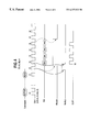
- FIG. 4 is a timing chart representing clock signal supply action
- FIG. 5 is another timing chart representing clock signal supply action.
- FIG. 6 is a circuit diagram of clock supply control signal generator circuit.
- FIG. 1 is an overall schematic diagram of an SDRAM in one aspect of an embodiment of the present invention.
- a memory cell array MCA comprises a plurality of word lines WL and bit lines BL and /BL, and memory cells each comprising one transistor and one capacitor at the intersections thereof. Row addresses in the row direction are loaded in by an address buffer 10 and decoded by a row decoder 12 , and a selected word line WL is driven. In conjunction with the driving of the word line WL, very small voltages corresponding to the stored data are generated on the bit lines BL and /BL, and those very small voltages are amplified by a sense amp SA that is connected to the bit line pair. The operation up to this point is the row side (RAS system) operation.
- RAS system row side
- Read data detected by the sense amp SA are selected by a column decoder 16 that decodes addresses loaded into a column address buffer 14 and output to a pair of data bus lines DB and /DB.
- the pair of data buses DB and /DB are amplified by a data bus amp 18 , and the amplified read data are supplied to a data output circuit 40 via a pipeline gate 20 and a data bus control circuit 22 .
- An internal data read circuit 30 is configured by the data bus amp 18 and the data bus control circuit 22 . This internal data read circuit 30 corresponds to a column-system internal read circuit after taking in a column address.
- the data output circuit 40 as well as a data input circuit (not shown) are connected to the I/O terminal DQ.
- To this data output circuit 40 are supplied read data from the internal read circuit 30 and a high-impedance control signal Hz for maintaining the transistors in the CMOS inverters 48 and 49 in the output stage in a high-impedance condition.
- the high-impedance control signal Hz is high (H)
- the output at the NOR gate 47 goes low (L)
- the output at the NAND gate 46 goes high (H)
- a high-impedance state is effected relative to the I/O terminal DQ.
- data are taken in on the data input circuit (not shown) side.
- the outputs at the NOR gate 47 and NAND gate 46 will be either high (H) or low (L) depending on the level of the read data DA, one or other of the transistors 48 and 49 will conduct, and the I/O terminal DQ will be driven.
- command control signals /CAS, /RAS, /WE, and /CS are supplied, from the outside, command control signals /CAS, /RAS, /WE, and /CS. These signals are decoded, and mode control signals (not shown) corresponding thereto are output and supplied to corresponding internal circuits to control the functioning thereof.
- One of the features of the SDRAM is that, in synchronization with the clock signal CLK, signals are taken in from the outside, the internal circuits are activated, and data are output to the outside. That being so, the clock signal CLK supplied from the outside, as diagrammed, is input by a clock input buffer 54 , amplified, and supplied as an internal clock signal I-CLK to the respective corresponding circuits. More specifically, a control clock signal CLK 1 is supplied to the data output circuit 40 via a first clock signal supply circuit 56 . In response to this control clock signal CLK 1 , gates 42 and 44 in the data output circuit 40 open, so that the read data DA and the high-impedance control signal Hz are supplied, and the data output circuit 40 is activated.
- a control clock signal CLK 2 via a second clock signal supply circuit 58 (comprising an inverter).
- the internal data read circuit 30 effects a pipeline configuration, and, in response to the control clock signal CLK 2 , the pipeline gate 20 is opened and the internal operation is synchronized with the clock signals.
- a control clock signal CLK 3 is supplied via a third clock signal supply circuit 60 to the address buffers 10 , 14 that inputs address signals. In this address buffers 10 , 14 , address signals Add from the outside are input, at the rising edge of the control clock signal CLK 3 .
- the clock signal CLK supplied from the outside is, when the non-power-down state is in effect, taken in, branched, and supplied to the data output circuit 40 , the internal data read circuit 30 , and the address buffers 10 , 14 , respectively, through the respective clock signal supply circuits.
- Each of these circuits, i.e. 40 , 30 , 10 , and 14 function in response to the control clock signals CLK 1 , CLK 2 , and CLK 3 , respectively, which are supplied thereto.
- the taking in of the external clock signal CLK is disabled by a power-down mode signal PD, whereupon no clock signal is supplied to the internal circuitry.
- FIG. 2 is given an overall diagram of a SDRAM chip.
- a chip 1 inside a chip 1 are comprised a group of I/O terminals DQ 0 -DQ 7 , data output circuits 40 corresponding thereto, a clock signal input terminal CLK, and a clock signal supply circuit 56 .
- multiple data I/O terminals DQ are deployed in a wide range inside the chip, each I/O terminal having a data output circuit 40 connected thereto.
- the clock signal supply circuit 56 in order for the clock signal CLK to be supplied to these data output circuits 40 , the clock signal supply circuit 56 must drive a clock signal supply line 70 over a long distance with a heavy load. It requires much current consumption to drive this clock signal supply line 70 because of its long length and large capacitive load.
- the control clock signal CLK 1 is supplied to the data output circuit 40 only during the time when read data need to be output from the data output circuit 40 during the time interval from the active status wherein an active command is supplied to the recharge status wherein a recharge command is supplied. Therefore, a NAND gate 63 is provided in the clock signal supply circuit 56 , to one input whereof is supplied the clock signal I-CLK, and to the other input whereof is supplied the output signal of the inverter 64 generated from the clock supply control signals Readz and Redcz.
- clock supply control signals Readz and Redcz go high (H), in a read status following an active status, to enable clock signal supply. In the active status or write status, for example, both of the clock supply control signals Readz and Redcz go low (L) to disable clock signal supply.
- the clock supply control signals Readz and Redcz while in the read status following reception of a read command, enter a clock signal supply enabled state (H level) after a clock period for a preset CAS latency after receiving the read command, and enter a clock signal supply disabled state (L level) after the output of read data for the burst length is finished.
- the CAS latency and burst length mentioned here are set beforehand in an upper-level memory controller. Accordingly, in response to this preset value, the start timing and end timing for the supply of clock signals to the data output circuit 40 is controlled so as to be optimized.
- FIG. 3 is a schematic diagram of a circuit for generating the clock supply control signals Readz and Redcz.
- the clock supply control signals Readz and Redcz are generated by a clock supply control signal generator circuit 72 .
- To the memory device are supplied control signals /CAS, /RAS, /WE, and ICS from the upper-level memory controller (not shown). These control signals are taken into an input buffer 74 synchronously with the control clock signal CLK 3 .
- These control signals are decoded in the command decoder 52 . More specifically, a combination of control signals is decoded by a decoder circuit comprising NAND gates, etc. (not shown), and the respective control signals are output.
- a read command signal READ, an interrupt signal INT, and a mode register set signal MRS are represented according to the control signals generated as a result of this decoding.
- a mode register setting circuit 76 in response to the mode register set signal MRS supplied from the command decoder 52 , sets the CAS latency value CL and the burst length value BL supplied from the data input terminal DATA in corresponding registers CL and BL inside a mode register 78 .
- the settings in this mode register 78 are normally made according to data from an upper-level memory device when power to the memory device is turned on.
- the CAS latency is the number of clock pulses from the reception of a read command to the output of the first read data from the I/O terminals DQ.
- the burst length is the number of continuous output data in the burst mode.
- the command decoder 52 detects that a read command has been received from a combination of control signals and outputs a read command signal READ.
- This read command signal READ is supplied to the clock supply control signal generator circuit 72 and prompts the generation of the clock supply control signals Readz, Redcz.
- the command decoder 52 also detects that a write command has been received from a combination of control signals and outputs both a write command signal (not shown) and an interrupt signal INT.
- This interrupt signal INT is supplied both to the internal circuitry (not shown) and to the clock supply control signal generator circuit 72 , and prompts termination of the clock supply control signals.
- the clock supply control signal generator circuit 72 latches the read command signal READ and, in response thereto, generates the clock supply control signals during an interval of time that accords with the CAS latency CL and the burst length BL, and enables the clock signal supply circuit 56 to supply the clock signal I-CLK. During other times, the supply of the clock signal I-CLK from the clock signal supply circuit 56 is disabled.
- FIG. 4 is a timing chart for the action of supplying clock signals.
- a clock signal CLK from the outside are taken in as the clock signal I-CLK.
- the internal clock signal I-CLK is supplied continuously as control clock signals CLK 2 , CLK 3 , etc., respectively, to the internal data read circuit 30 and the address buffer 14 , etc.
- an active command ACTIVE is supplied, after which, at time t1, a read command READ is supplied.
- ACTIVE a row address is loaded, and the word line WL is selected and driven by the row decoder 12 .
- the very small voltages generated on the pair of bit lines BL and /BL are detected and amplified by the sense amp SA.
- a column address is loaded into the address buffer 14 , a column is selected by the column decoder 16 , and the output of the sense amp SA for the selected column is connected to the pair of data bus lines DB and /DB.
- a pipeline gate inside the internal data read circuit 30 that is a CAS-system circuit opens in response to the control clock signal CLK 2 , and a data read operation is performed.
- the data output circuit 40 outputs the read data DA 0 .
- the control clock signal CLK 1 be supplied during the time period from t3 to t6 wherein at least the read data DA 0 -DA 3 are output.
- the second clock supply control signal Redcz is raised to the H level only during the interval of one clock period from the rising edge at time t2.
- the H levels of these clock supply control signals are supplied to the clock signal supply circuit 56 , pass through the NOR gate 65 and the inverter 64 , and open the NAND gate 63 , whereupon supply of the clock signal I-CLK is enabled.
- the supply of the control clock signal CLK 1 to the data output circuit 40 begins from time t3.
- the details of the configuration of the clock signal supply circuit 56 are diagrammed in FIG. 3 .
- This configuration specifically, comprises a gate 66 that opens when the clock signal I-CLK is low (L), and a latching circuit 67 that latches the output of the NOR gate 65 . Accordingly, in the example diagrammed in FIG.
- the H level of the second clock supply control signal Redcz generated in response to the rising edge of the clock signal at time t2 is latched in the latching circuit 67 at the next falling edge of the clock pulse.
- the NAND gate 63 opens. Accordingly, the supply of the clock signal I-CLK begins without fail at the rising edge at time t3.
- the first clock supply control signal Readz is high (H), wherefore, in like manner, the open state of the NAND gate 63 is maintained, and the supply of the control clock signal CLK 1 thereafter is continued. Due to the configuration of the internal circuitry, after time t2, even when the change to the H level of the first clock supply control signal Readz is delayed, the control signal Redczs will have become high (H) for the one clock period prior thereto, wherefore the supply of the clock signal CLK 1 will begin without fail at time t3.
- the clock supply control signal generator circuit 72 generates clock supply control signals with reference to a preset CAS latency CL and burst length BL, so that the control clock signal CLK 1 is only supplied to the data output circuit 40 during the time period when read data DA 0 -DA 3 are being output. It also generates clock supply control signals so that the supply of the control clock signal CLK 1 is disabled at all other times. Accordingly, the number of times that the control clock signal CLK 1 is driven is held to a minimum, and the large current consumption associated with this drive is also reduced to a minimum.
- FIG. 5 is another timing chart for the action of supplying clock signals.
- the external clock signal CLK is taken into the internal circuitry as the internal clock signal I-CLK, and, irrespective of the read status being in effect, the control clock signals CLK 2 and CLK 3 are supplied continuously to the internal data read circuit 30 and address buffer 14 , etc.
- the waveform of the first clock supply control signal Readz when a write command WRITE is supplied at the rising edge of the clock signal at time t7 while the burst read operation is indicated by a broken line.
- the command decoder 52 when a write command WRITE is supplied at the rising edge of the clock signal at time t7, the command decoder 52 generates a write command signal (not shown) and, at the same time, generates an interrupt signal INT.
- the generation of this write command means that the read operation is canceled thereafter and a write operation will be performed. Accordingly, after the reception of the write command, it is no longer necessary to supply the control clock signal CLK 1 to the data output circuit 40 . That being so, in response to this interrupt signal INT, the clock supply control signal generator circuit 72 controls the first clock supply control signal Readz so that it goes low (L). As a result, the supply of the control clock signal CLK 1 from time t8 on is stopped.
- the clock supply control signal generator circuit 72 diagrammed in FIG. 3 latches the read command signal READ, so that the level of the clock supply control signal goes high (H) in response thereto, whereby the control clock signal CLK 1 can be supplied to the data output circuit 40 only during the time period that the read status is in effect.
- the supply of the control clock signal CLK 1 can be stopped by having the latched state of the read command signal READ released by another command signal, for example.
- current consumption can be further reduced by having the clock supply control signal generator circuit 72 reference the CAS latency CL and burst length BL, and supply the control clock signal CLK 1 only while read data DA from the data output circuit 40 is actually being output with the read status in effect.
- FIG. 6 is a circuit diagram of the clock supply control signal generator circuit.
- the clock supply control signal generator circuit 72 includes a CL counter for generating the second clock supply control signal Redcz and a BL counter for generating the first clock supply control signal Readz.
- the read command signal READ, the interrupt signal INT and the internal clock I-CLK are supplied to the clock supply control signal generator circuit 72 .
- the CAS latency signals CL 2 and CL 3 are supplied to the CL counter.
- the CAS latency signals CL 2 and CL 3 become H level when the CAS latency is 2 and 3 respectively.
- the burst length signals BL 1 , BL 2 , BL 3 , BL 4 , . . . BL 16 are supplied to the BL counter and become H level when the burst length is 1, 2, 3, 4,. . . 16 respectively.
- the CL counter comprises transfer gates 101 , 102 , 103 and 104 and latch circuits L 101 , L 102 , L 103 and L 104 .
- the H level read command signal READ is transferred to each latch circuit L 101 , L 103 via the transfer gates 101 and 103 in response to a falling edge of the internal clock I-CLK, and also is transferred to each latch circuit L 102 , L 104 via the transfer gates 102 and 104 in response to a rising edge of the internal clock I-CLK.
- the H level control signal Redcz is latched by a latch circuit comprised by NOR gates 94 and 95 so that the first clock supply control signal Readz becomes H level. Therefore, as shown in FIG. 4 (FIG. 5 ), the control signal Readz becomes H level in response to the rising edge of the internal clock I-CLK at t2 (t3).
- the BL counter has the similar clock transfer circuit as the CL counter.
- Transfer gates 105 , 107 , 109 , 111 , 113 , . . . are conductive so as to transfer the control signal Redcz in response to each falling edge of the internal clock I-CLK.
- Transfer gates 106 , 108 , 110 , 112 , . . . are conductive in response to each rising edge of the internal clock I-CLK.
- latch circuits L 105 -L 112 are provided between the transfer gates.
- the transfer gates 106 , 108 , 110 and 112 transfer the H level second control signal Redcz to the following latch circuit L 106 , L 108 , L 110 and L 112 at t3, t4, t5, t6 respectively, and the NAND gate 92 output H level when the latch circuit L 112 holds the H level Redcz. Then, output of NAND gate 93 resets the latch circuit made by 94 and 95 so as to cause the first clock supply control signal Readz L level.
- the BL counter causes the first clock supply control signal Readz L level in the timing set by the burst length signal BL 1 -BL 16 .
- the interrupt signal INT becomes H level in response to the write command WRITE
- the second control signal Redcz becomes L level via the latch circuits L 102 , L 104 by the interrupt signal INT so that the first control signal Readz also becomes L level thereafter.
- consumption of the drive current associated with the supply of control clock signals in a clock-synchronized memory device can be reduced by limiting the period of control clock signal supply to the data output circuit to the time that a read status is in effect.
- the drive current associated with the supply of control clock signals in a clock-synchronized memory device can be further reduced by limiting the supply of control clock signals to the data output circuit in such manner that the supply of control clock signals is limited only to periods that are further limited, in accordance to a preset CAS latency and burst length, when in the read status.
Landscapes
- Engineering & Computer Science (AREA)
- Microelectronics & Electronic Packaging (AREA)
- Computer Hardware Design (AREA)
- Dram (AREA)
Abstract
Description
Claims (8)
Applications Claiming Priority (2)
| Application Number | Priority Date | Filing Date | Title |
|---|---|---|---|
| JP10198590A JP2000030456A (en) | 1998-07-14 | 1998-07-14 | Memory device |
| JP10-198590 | 1998-07-14 |
Publications (1)
| Publication Number | Publication Date |
|---|---|
| US6337833B1 true US6337833B1 (en) | 2002-01-08 |
Family
ID=16393729
Family Applications (1)
| Application Number | Title | Priority Date | Filing Date |
|---|---|---|---|
| US09/346,919 Expired - Lifetime US6337833B1 (en) | 1998-07-14 | 1999-07-02 | Memory device |
Country Status (3)
| Country | Link |
|---|---|
| US (1) | US6337833B1 (en) |
| JP (1) | JP2000030456A (en) |
| KR (1) | KR100573534B1 (en) |
Cited By (11)
| Publication number | Priority date | Publication date | Assignee | Title |
|---|---|---|---|---|
| US20030046599A1 (en) * | 2001-08-31 | 2003-03-06 | Kabushiki Kaisha Toshiba | Apparatus for controlling card device and clock control method |
| US6564287B1 (en) * | 2000-08-18 | 2003-05-13 | Samsung Electronics Co., Ltd. | Semiconductor memory device having a fixed CAS latency and/or burst length |
| US20030163749A1 (en) * | 2002-02-26 | 2003-08-28 | Sun Microsystems, Inc. | Modified glitch latch for use with power saving dynamic register file structures |
| US20030185088A1 (en) * | 2002-03-29 | 2003-10-02 | Mitsubishi Denki Kabushiki Kaisha | Semiconductor memory device with internal clock generation circuit |
| US6898683B2 (en) * | 2000-12-19 | 2005-05-24 | Fujitsu Limited | Clock synchronized dynamic memory and clock synchronized integrated circuit |
| US20070291572A1 (en) * | 2006-06-20 | 2007-12-20 | Josef Schnell | Clock circuit for semiconductor memory |
| US20100265780A1 (en) * | 2009-04-20 | 2010-10-21 | Samsung Electronics Co., Ltd. | Semiconductor memory device having reduced power consumption during latency |
| US20100278004A1 (en) * | 2007-05-14 | 2010-11-04 | Hynix Semiconductor Inc. | Address receiving circuit for a semiconductor apparatus |
| US20120210157A1 (en) * | 2009-11-05 | 2012-08-16 | Rambus Inc. | Interface clock management |
| US10437514B2 (en) | 2017-10-02 | 2019-10-08 | Micron Technology, Inc. | Apparatuses and methods including memory commands for semiconductor memories |
| US10467158B2 (en) * | 2017-11-29 | 2019-11-05 | Micron Technology, Inc. | Apparatuses and methods including memory commands for semiconductor memories |
Families Citing this family (8)
| Publication number | Priority date | Publication date | Assignee | Title |
|---|---|---|---|---|
| JP2001014847A (en) * | 1999-06-30 | 2001-01-19 | Toshiba Corp | Clock synchronization circuit |
| JP3535788B2 (en) * | 1999-12-27 | 2004-06-07 | Necエレクトロニクス株式会社 | Semiconductor storage device |
| JP2002109880A (en) * | 2000-09-28 | 2002-04-12 | Toshiba Corp | Clock synchronization circuit |
| KR100638747B1 (en) * | 2004-12-28 | 2006-10-30 | 주식회사 하이닉스반도체 | Apparatus and method for generating clock of semiconductor memory device |
| KR100744042B1 (en) * | 2005-09-28 | 2007-07-30 | 주식회사 하이닉스반도체 | Internal address generator of semiconductor memory device |
| US7489172B2 (en) * | 2005-09-29 | 2009-02-10 | Hynix Semiconductor Inc. | DLL driver control circuit |
| US7609584B2 (en) | 2005-11-19 | 2009-10-27 | Samsung Electronics Co., Ltd. | Latency control circuit and method thereof and an auto-precharge control circuit and method thereof |
| KR20110052941A (en) | 2009-11-13 | 2011-05-19 | 삼성전자주식회사 | Semiconductor device with additive latency |
Citations (5)
| Publication number | Priority date | Publication date | Assignee | Title |
|---|---|---|---|---|
| US5768213A (en) * | 1995-06-30 | 1998-06-16 | Samsung Electronics Co., Ltd. | Clock generating circuit for use in semiconductor memory device |
| US5893925A (en) * | 1995-12-25 | 1999-04-13 | Mitsubishi Denki Kabushiki Kaisha | Synchronous semiconductor memory device in which burst counter is commonly employed for data writing and for data reading |
| US5930198A (en) * | 1996-12-20 | 1999-07-27 | Micron Technology, Inc. | Memory having a plurality of external clock signal inputs |
| US5959900A (en) * | 1996-08-09 | 1999-09-28 | Nec Corporation | Synchronous semiconductor memory having a reduced number of registers |
| US6064627A (en) * | 1996-09-26 | 2000-05-16 | Mitsubishi Denki Kabushiki Kaisha | Synchronous semiconductor memory device |
Family Cites Families (6)
| Publication number | Priority date | Publication date | Assignee | Title |
|---|---|---|---|---|
| KR0164807B1 (en) * | 1995-12-22 | 1999-02-01 | 김광호 | Data Output Buffer Control Circuit of Semiconductor Memory Device |
| KR980004976A (en) * | 1996-06-07 | 1998-03-30 | 김광호 | Clock generation controller and clock generation control method of semiconductor memory device |
| JPH10208470A (en) * | 1997-01-17 | 1998-08-07 | Nec Corp | Synchronous semiconductor memory device |
| KR100240419B1 (en) * | 1997-03-18 | 2000-01-15 | 윤종용 | Data reading method and semiconductor memory device for reducing current consumed at a reading operation |
| JP3504104B2 (en) * | 1997-04-03 | 2004-03-08 | 富士通株式会社 | Synchronous DRAM |
| KR100258859B1 (en) * | 1997-04-30 | 2000-06-15 | 김영환 | Data output buffer in memory |
-
1998
- 1998-07-14 JP JP10198590A patent/JP2000030456A/en active Pending
-
1999
- 1999-07-02 US US09/346,919 patent/US6337833B1/en not_active Expired - Lifetime
- 1999-07-13 KR KR1019990028147A patent/KR100573534B1/en not_active Expired - Fee Related
Patent Citations (5)
| Publication number | Priority date | Publication date | Assignee | Title |
|---|---|---|---|---|
| US5768213A (en) * | 1995-06-30 | 1998-06-16 | Samsung Electronics Co., Ltd. | Clock generating circuit for use in semiconductor memory device |
| US5893925A (en) * | 1995-12-25 | 1999-04-13 | Mitsubishi Denki Kabushiki Kaisha | Synchronous semiconductor memory device in which burst counter is commonly employed for data writing and for data reading |
| US5959900A (en) * | 1996-08-09 | 1999-09-28 | Nec Corporation | Synchronous semiconductor memory having a reduced number of registers |
| US6064627A (en) * | 1996-09-26 | 2000-05-16 | Mitsubishi Denki Kabushiki Kaisha | Synchronous semiconductor memory device |
| US5930198A (en) * | 1996-12-20 | 1999-07-27 | Micron Technology, Inc. | Memory having a plurality of external clock signal inputs |
Cited By (29)
| Publication number | Priority date | Publication date | Assignee | Title |
|---|---|---|---|---|
| US6564287B1 (en) * | 2000-08-18 | 2003-05-13 | Samsung Electronics Co., Ltd. | Semiconductor memory device having a fixed CAS latency and/or burst length |
| US6898683B2 (en) * | 2000-12-19 | 2005-05-24 | Fujitsu Limited | Clock synchronized dynamic memory and clock synchronized integrated circuit |
| US20030046599A1 (en) * | 2001-08-31 | 2003-03-06 | Kabushiki Kaisha Toshiba | Apparatus for controlling card device and clock control method |
| US6990599B2 (en) * | 2001-08-31 | 2006-01-24 | Kabushiki Kaisha Toshiba | Method and apparatus of clock control associated with read latency for a card device |
| US6981169B2 (en) * | 2002-02-26 | 2005-12-27 | Sun Microsystems, Inc. | Modified glitch latch for use with power saving dynamic register file structures |
| US20030163749A1 (en) * | 2002-02-26 | 2003-08-28 | Sun Microsystems, Inc. | Modified glitch latch for use with power saving dynamic register file structures |
| US20030185088A1 (en) * | 2002-03-29 | 2003-10-02 | Mitsubishi Denki Kabushiki Kaisha | Semiconductor memory device with internal clock generation circuit |
| US6768698B2 (en) * | 2002-03-29 | 2004-07-27 | Renesas Technology Corp. | Semiconductor memory device with internal clock generation circuit |
| US20070291572A1 (en) * | 2006-06-20 | 2007-12-20 | Josef Schnell | Clock circuit for semiconductor memory |
| US20100278004A1 (en) * | 2007-05-14 | 2010-11-04 | Hynix Semiconductor Inc. | Address receiving circuit for a semiconductor apparatus |
| US8059483B2 (en) * | 2007-05-14 | 2011-11-15 | Hynix Semiconductor Inc. | Address receiving circuit for a semiconductor apparatus |
| US20100265780A1 (en) * | 2009-04-20 | 2010-10-21 | Samsung Electronics Co., Ltd. | Semiconductor memory device having reduced power consumption during latency |
| US8228748B2 (en) | 2009-04-20 | 2012-07-24 | Samsung Electronics Co., Ltd. | Semiconductor memory device having reduced power consumption during latency |
| US9824056B2 (en) * | 2009-11-05 | 2017-11-21 | Rambus Inc. | Handshake signaling for interface clock management |
| US11238003B2 (en) | 2009-11-05 | 2022-02-01 | Rambus Inc. | Interface clock management |
| US12346283B2 (en) * | 2009-11-05 | 2025-07-01 | Rambus Inc. | Interface clock management |
| US12032508B2 (en) | 2009-11-05 | 2024-07-09 | Rambus Inc. | Interface clock management |
| US10558608B2 (en) | 2009-11-05 | 2020-02-11 | Rambus Inc. | Interface clock management |
| US11681648B2 (en) | 2009-11-05 | 2023-06-20 | Rambus Inc. | Interface clock management |
| US20120210157A1 (en) * | 2009-11-05 | 2012-08-16 | Rambus Inc. | Interface clock management |
| US11262941B2 (en) | 2017-10-02 | 2022-03-01 | Micron Technology, Inc. | Apparatuses and methods including memory commands for semiconductor memories |
| US10437514B2 (en) | 2017-10-02 | 2019-10-08 | Micron Technology, Inc. | Apparatuses and methods including memory commands for semiconductor memories |
| US10915474B2 (en) | 2017-11-29 | 2021-02-09 | Micron Technology, Inc. | Apparatuses and methods including memory commands for semiconductor memories |
| US11347666B2 (en) | 2017-11-29 | 2022-05-31 | Micron Technology, Inc. | Apparatuses and methods including memory commands for semiconductor memories |
| US11550741B2 (en) | 2017-11-29 | 2023-01-10 | Micron Technology, Inc. | Apparatuses and methods including memory commands for semiconductor memories |
| US10789186B2 (en) * | 2017-11-29 | 2020-09-29 | Micron Technology, Inc. | Apparatuses and methods including memory commands for semiconductor memories |
| US12019570B2 (en) | 2017-11-29 | 2024-06-25 | Micron Technology, Inc. | Apparatuses and methods including memory commands for semiconductor memories |
| US10467158B2 (en) * | 2017-11-29 | 2019-11-05 | Micron Technology, Inc. | Apparatuses and methods including memory commands for semiconductor memories |
| US12197355B2 (en) | 2017-11-29 | 2025-01-14 | Micron Technology, Inc. | Apparatuses and methods including memory commands for semiconductor memories |
Also Published As
| Publication number | Publication date |
|---|---|
| JP2000030456A (en) | 2000-01-28 |
| KR20000011667A (en) | 2000-02-25 |
| KR100573534B1 (en) | 2006-04-26 |
Similar Documents
| Publication | Publication Date | Title |
|---|---|---|
| US6337833B1 (en) | Memory device | |
| US6064625A (en) | Semiconductor memory device having a short write time | |
| KR100702975B1 (en) | Semiconductor devices | |
| US6260128B1 (en) | Semiconductor memory device which operates in synchronism with a clock signal | |
| US5696729A (en) | Power reducing circuit for synchronous semiconductor device | |
| US7471578B2 (en) | Internal voltage generation control circuit and internal voltage generation circuit using the same | |
| US5535171A (en) | Data output buffer of a semiconducter memory device | |
| JP2003249077A (en) | Semiconductor memory device and its control method | |
| JPH08279282A (en) | Integrated circuit memory | |
| CN114582389B (en) | System and method for controlling data strobe signals during read operations | |
| JPH09231767A (en) | Static semiconductor memory device | |
| US6636443B2 (en) | Semiconductor memory device having row buffers | |
| KR100200763B1 (en) | Column Select Line Enable Circuit of Semiconductor Memory Device | |
| US6341100B1 (en) | Semiconductor integrated circuit having circuit for writing data to memory cell | |
| US7154316B2 (en) | Circuit for controlling pulse width | |
| US7961528B2 (en) | Buffer control circuit of memory device | |
| KR19980018015A (en) | Internal Operating Frequency Configurable DRAM | |
| US6545924B2 (en) | Semiconductor memory device | |
| JPH0991956A (en) | Semiconductor memory | |
| USRE36532E (en) | Synchronous semiconductor memory device having an auto-precharge function | |
| US6580656B2 (en) | Semiconductor memory device having memory cell block activation control circuit and method for controlling activation of memory cell blocks thereof | |
| JPH09245476A (en) | Semiconductor memory device | |
| US6005822A (en) | Bank selectable Y-decoder circuit and method of operation | |
| JP4112754B2 (en) | Semiconductor memory device | |
| KR100557970B1 (en) | I / O buffer |
Legal Events
| Date | Code | Title | Description |
|---|---|---|---|
| AS | Assignment |
Owner name: FUJITSU LIMITED, JAPAN Free format text: ASSIGNMENT OF ASSIGNORS INTEREST;ASSIGNORS:KANAZASHI, KAZUYUKI;UCHIDA, TOSHIYA;OKUDA, MASAKI;REEL/FRAME:010094/0828 Effective date: 19990628 |
|
| STCF | Information on status: patent grant |
Free format text: PATENTED CASE |
|
| FEPP | Fee payment procedure |
Free format text: PAYOR NUMBER ASSIGNED (ORIGINAL EVENT CODE: ASPN); ENTITY STATUS OF PATENT OWNER: LARGE ENTITY |
|
| CC | Certificate of correction | ||
| FPAY | Fee payment |
Year of fee payment: 4 |
|
| AS | Assignment |
Owner name: FUJITSU MICROELECTRONICS LIMITED, JAPAN Free format text: ASSIGNMENT OF ASSIGNORS INTEREST;ASSIGNOR:FUJITSU LIMITED;REEL/FRAME:021998/0645 Effective date: 20081104 Owner name: FUJITSU MICROELECTRONICS LIMITED,JAPAN Free format text: ASSIGNMENT OF ASSIGNORS INTEREST;ASSIGNOR:FUJITSU LIMITED;REEL/FRAME:021998/0645 Effective date: 20081104 |
|
| FPAY | Fee payment |
Year of fee payment: 8 |
|
| AS | Assignment |
Owner name: FUJITSU SEMICONDUCTOR LIMITED, JAPAN Free format text: CHANGE OF NAME;ASSIGNOR:FUJITSU MICROELECTRONICS LIMITED;REEL/FRAME:024982/0245 Effective date: 20100401 |
|
| FPAY | Fee payment |
Year of fee payment: 12 |
|
| AS | Assignment |
Owner name: SOCIONEXT INC., JAPAN Free format text: ASSIGNMENT OF ASSIGNORS INTEREST;ASSIGNOR:FUJITSU SEMICONDUCTOR LIMITED;REEL/FRAME:035508/0637 Effective date: 20150302 |