US6309049B1 - Printing apparatus and method for imaging charged toner particles using direct writing methods - Google Patents
Printing apparatus and method for imaging charged toner particles using direct writing methods Download PDFInfo
- Publication number
- US6309049B1 US6309049B1 US09/239,604 US23960499A US6309049B1 US 6309049 B1 US6309049 B1 US 6309049B1 US 23960499 A US23960499 A US 23960499A US 6309049 B1 US6309049 B1 US 6309049B1
- Authority
- US
- United States
- Prior art keywords
- toner
- packet
- electrodes
- packets
- printing apparatus
- Prior art date
- Legal status (The legal status is an assumption and is not a legal conclusion. Google has not performed a legal analysis and makes no representation as to the accuracy of the status listed.)
- Expired - Fee Related
Links
Images


Classifications
-
- G—PHYSICS
- G03—PHOTOGRAPHY; CINEMATOGRAPHY; ANALOGOUS TECHNIQUES USING WAVES OTHER THAN OPTICAL WAVES; ELECTROGRAPHY; HOLOGRAPHY
- G03G—ELECTROGRAPHY; ELECTROPHOTOGRAPHY; MAGNETOGRAPHY
- G03G15/00—Apparatus for electrographic processes using a charge pattern
- G03G15/22—Apparatus for electrographic processes using a charge pattern involving the combination of more than one step according to groups G03G13/02 - G03G13/20
- G03G15/34—Apparatus for electrographic processes using a charge pattern involving the combination of more than one step according to groups G03G13/02 - G03G13/20 in which the powder image is formed directly on the recording material, e.g. by using a liquid toner
- G03G15/344—Apparatus for electrographic processes using a charge pattern involving the combination of more than one step according to groups G03G13/02 - G03G13/20 in which the powder image is formed directly on the recording material, e.g. by using a liquid toner by selectively transferring the powder to the recording medium, e.g. by using a LED array
- G03G15/348—Apparatus for electrographic processes using a charge pattern involving the combination of more than one step according to groups G03G13/02 - G03G13/20 in which the powder image is formed directly on the recording material, e.g. by using a liquid toner by selectively transferring the powder to the recording medium, e.g. by using a LED array using a stylus or a multi-styli array
Definitions
- This invention relates to electrostatic printing, and more particularly to a direct wiring method and apparatus and methods for imaging charged toner particles directly to a print receiving medium.
- electrophotography has dominated high resolution monochrome printing for several decades.
- the electrophotographic process includes uniformly coating a photoconductive surface with charge, selectively exposing the charged surface with light to form a latent image, developing the latent image by causing charged toner particles to come in contact with it, transferring the image to a receiving sheet, and fixing the image.
- This printing method has produced high quality printing and has been refined to effectively service a broad range of printing applications. However, it is mechanically complex, requires precision optical components, and has proven difficult to adapt to color printing.
- Direct Electrostatic Printing can be simpler than electrophotographic printing.
- Pressman et al. disclose a DEP device in which toner is deposited directly through apertures onto a plain paper substrate in image configuration. This method has been improved by Schmidlin in U.S. Pat. No. 4,912,489 issued Mar. 27, 1990 in which a control voltage as low as 100 V is sufficient to modulate the flow of toner through the apertures.
- the Schmidlin device employs a traveling wave conveyor to present toner to the print head apertures.
- U.S. Pat. No. 3,113,042 issued to Hall in 1963 describes a magnetic toner conveyor for use as a developer unit in a xerographic printer.
- Magnetic powder is transported from a toner reservoir to develop a latent image on a xerographic plate or drum.
- the conveyor has a linear structure with multiple phases driven by current sources to magnetically convey the toner.
- U.S. Pat. No. 3,778,678 issued to Masuda in 1974 describes a voltage traveling wave device for moving particles along a tubular duct.
- the electrodes are spirally wound along the outer surface and are connected to a three-phase alternating current source of 5-10 kV, which repels the particles from the inner surface and propels them along the tube.
- Masuda also describes a grid of planar spaced-apart electrodes covering the wall of a paint booth for transporting paint particles for the purpose of removing paint from the wall.
- U.S. Pat. No. 4,527,884 issued to Nusser in 1985 describes a device for applying toner to an electrostatic charge image carried on an information carrier.
- the apparatus employs a traveling wave conveyor to transport the toner in the form of an aerosol to the information carrier where a development gap is created between the surface of the traveling wave conveyor and the information carrier. Toner is transferred across the gap to the information carrier to develop the image.
- U.S. Pat. No. 4,568 issued to Hosoya et al.
- the present invention builds on the concept of direct writing heads employing voltage traveling waves. It describes an electrostatic toner loading apparatus and method to create a convenient source of charged toner at the surface of a planar member.
- the loading method causes toner particles mixed with air to periodically sweep the planar surface. The particles are available for imaging at the surface of the planar member.
- a feature of this approach is that the thin film circuits on the planar surface that create the toner loading action can co-exist and co-function with circuits on the same planar surface that are used to image the particles. Further, it will be shown that the imaging circuits can form images by either additive or subtractive means, providing a broad range of printer design solutions.
- barrier electrodes to channel the toner flow into pixel-wide columns corresponding to the pixels across the image formed on a receiving sheet.
- Toner flow in each channel may be individually modulated to further create pixels in the process direction and gray-levels within each pixel.
- the barrier electrodes help to keep toner packets segregated into pixel-wide columns and prevent crosstalk between adjacent channels.
- the barrier electrodes channelize toner transport on a surface, and minimize cross-talk between the channels.
- Cyclotene has the desirable property of being essentially triboelectrically neutral to charged toner touching events. As toner is transported along a traveling wave channel, some of the particles touch or slide against the supporting surface. If touching or sliding events changed the particle charge, it would be difficult to repeatably control the charge on toner particles and therefore the electrostatic force. Conversely, if the touching events are charge neutral, the charge to mass ratio of the particles remains relatively constant, and the fields asserted by the voltage traveling waves and the imaging electrodes control and move the toner in consistent and predictable ways.
- Hosoya et al. describe a xerographic developer unit for single component non-magnetic toner employing a regulating plate pressed against a donor roll to meter the toner into a thin layer and to charge it triboelectrically. They describe its use in non-contact development of a photoconductive drum. The effects of surface roughness, plate pressure, and bias voltage are described.
- a similar device serves as a loading apparatus.
- what is needed is well charged toner that can be presented to a writing head.
- Another object of the present invention is to create a method for electrostatically loading toner particles that provides a periodic brushing action of charged toner particles against a receiving surface that can be further configured with toner imaging structures. It is a related object to provide the toner particles in a form that is easily imaged, namely in an aerosol of toner particles mixed with air. A further object of the loading method is to manage wrong sign toner, WST, in a manner that prevents WST from reaching and interacting with the writing head.
- a printing system that employs direct writing heads; each contained in a print cartridge.
- Each print cartridge includes a toner cartridge, a toner charging cartridge, and a writing head, and each of these can be separately replaced.
- a print cartridge is provided for each of the process colors: cyan, yellow, magenta, and black. They are assembled within a precision frame to provide a four-color writing head module.
- Each writing head is capable of continuously imaging toner, which streams off a transfer edge to a receiving sheet.
- a single black-and-white writing head or a four-color writing head module is positioned above a dielectric belt.
- the dielectric belt carries a print-receiving medium such as paper or transparency, such that the medium is precisely located opposite the transfer points of the one or more writing heads.
- Mechanisms are provided to compensate for varying medium thickness.
- blank sheets are retrieved from paper trays or from a bypass feed for thick sheets.
- the bypass feed employs a straight paper path that is desirable for stiff printing substrates, to avoid bending the substrate during paper feeding.
- the print receiving sheet separates from the dielectric belt and passes through a fuser, and is subsequently ejected from the print engine.
- the printing method of the current invention includes four steps: imaging, transporting, transferring, and fixing.
- the imaging step causes toner from a suitable source to form into image-bearing toner packets on a writing head.
- the transport step conveys the image-bearing toner packets on the writing head to a transfer region adjacent the image-receiving member.
- the transfer step causes the toner packets to transfer from the writing head to the image-receiving member, while maintaining the integrity of the image.
- the fixing step fuses the toner to the image-receiving member.
- the printing system is compatible with optional input devices such as a high capacity input device, and also with optional output devices such as sorters, staplers, booklet makers, and other finishing devices.
- optional input devices such as a high capacity input device
- optional output devices such as sorters, staplers, booklet makers, and other finishing devices.
- the four-color engine can be located adjacent to a computer system board connected to an operator console, with convenient access to all the components that may require service.
- An optional scanning device may be added to provide the capability to print copies from optical originals.
- the ability to transport toner near a surface using voltage traveling waves, and to digitally image the toner particles as they move along a traveling wave structure, is a powerful and general capability.
- the apparatus and methods described herein can be applied to build printers that are fast because of their parallel architectures and precise because they implement digital imaging algorithms.
- most of the printing functions are implemented electronically rather than in optical or electromechanical parts, there are several cost-related benefits.
- the development time for creation of a solid state printer of the present invention can be much shorter than for xerographic printers. This is because the methods for developing integrated circuits (ICs) and electronic assemblies are highly developed by the semiconductor and computer manufacturing industries.
- the cost per function can be improved because of the generally lower cost per function of the electronic components compared with their electromechanical equivalents.
- the cost of the printing system can be reduced over time using time-proven learning curves for yield improvement and cost reduction of the electronic components and their methods of assembly and testing.
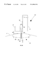
- FIG. 1 is a schematic, side-elevational illustration of an apparatus representing a print cartridge of the present invention, including a toner charging cartridge, toner, and a writing head assembly.
- FIG. 2 is a schematic side-elevational view of a printing head showing three processing regions of the present invention: image, transport, and transfer.
- FIG. 3A is a schematic plan view of a writing head of the present invention with separate integrated circuit chips mounted on the flat panel.
- FIG. 3B is a schematic plan view of a writing head of the present invention, with the separate integrated circuit chips replaced by active transistor circuits that are integrated with the thin film structure.
- FIG. 4 is a schematic side-elevational illustration of a four-color print apparatus of the present invention employing four print cartridges.
- FIG. 5 is a schematic front-elevational view of a printing system of the present invention.
- FIG. 6A is a cross-sectional illustration of a toner particle of the polymerized type.
- FIG. 6B is a cross-sectional illustration of several toner particles of the attrited type.
- FIG. 7A is a plan layout view of a print head traveling wave channel.
- FIG. 7B is a side-elevational view of a print head traveling wave channel with associated toner packets.
- FIG. 7C is a graph of voltage versus time for example waveforms of a voltage traveling wave applied to the electrodes of the traveling wave channel implemented with eight phases.
- FIG. 8A is a schematic plan view of a pixel site at 600 pixels per inch, implemented with binary dots at 2400 dots per inch (dpi) representative of offset printing.
- FIG. 8B is a plan view of a pixel site of the present invention, also at 600 pixels per inch.
- FIG. 9A is a schematic side-elevational view of an electrostatic loading apparatus of the present invention.
- FIG. 9B is an enlarged side-elevational view of the development gap region of FIG. 9 A.
- FIG. 9C is a graph of voltage versus time for an example waveform for the digital voltage bias element shown in FIG. 9 A.
- FIG. 9D is a schematic plan view of the thin film structure associated with an electrostatic loading apparatus of the present invention, represented by portion DD of FIG. 9 B.
- FIG. 10A is a plan view of spaced-apart elongated electrodes used to illustrate additive imaging.
- FIG. 10B is a graph of surface potential versus distance at the section WW of FIG. 10A, illustrating a potential well in the form of a trough that captures toner particles.
- FIG. 10C is a side-elevational view of a pile of toner particles captured by the potential well of FIG. 10 B.
- FIG. 10D is an expanded view of a portion of the thin film structure of FIG. 9D with the addition of additive imaging electrodes, and shows partially completed toner packets imaged by an additive process.
- FIG. 10E is a graph of surface potential versus distance at section VV of FIG. 10 D.
- FIG. 10F is a side-elevational view of variably sized toner piles corresponding to the potential wells of FIG. 10 E.
- FIG. 10G is a plan view illustration of a time sequence of packet forming events using the additive imaging process.
- FIG. 11A is a side-elevational view of a toner packet passing over a diverter electrode.
- FIG. 11B is a side elevational view of two sub-packets formed by diverter action.
- FIG. 11C shows a profile of toner mass versus time for a packet.
- FIG. 11D is a plan view illustration of a time sequence of packet forming events using the subtractive imaging process.
- FIG. 12 shows an example of a diverter waveform as a plot of voltage versus time.
- FIG. 13 shows computer simulated transfer functions for a diverter.
- FIG. 14A shows an expanded plan view of a portion of a traveling wave channel, showing straight phase electrodes and a straight diverter electrode.
- FIG. 14B shows an expanded plan view of a portion of a traveling wave channel, showing straight phase electrodes and a slanted diverter electrode.
- FIG. 14C shows an expanded plan view of a portion of a traveling wave channel, showing straight phase electrodes and a triangular diverter electrode shaped symmetrically to the toner path.
- FIG. 14D shows an expanded plan view of a portion of a traveling wave channel, showing straight phase electrodes and a right-triangle-shaped diverter electrode.
- FIG. 14E shows an expanded plan view of a portion of a traveling wave channel, showing phase electrodes with a chevron shape and a straight diverter electrode.
- FIG. 15A is a side-elevational view of a transfer subsystem of the present invention, including an opposing print head.
- FIG. 15B is an expanded plan view of the portion BB of FIG. 15 A.
- FIG. 16A is a schematic side-elevational illustration of the toner path from donor roll to receiving sheet, showing the sub-processes encountered by the toner particles.
- FIG. 16B is an expanded plan view of a portion of the thin film structure designated BB in FIG. 16A, showing the details for additive imaging.
- FIG. 16C is an expanded plan view of a portion of the thin film structure designated CC in FIG. 16 A.
- FIG. 16D is an expanded plan view of a portion of the thin film structure designated DD in FIG. 16 A.
- FIG. 16E is an expanded plan view of a portion of the thin film structure designated BB in FIG. 16A, with the details shown for subtractive imaging instead of additive imaging.
- FIG. 17A shows the connecting traces from high voltage drivers to diverter electrodes for the un-multiplexed case.
- FIG. 17B shows the connecting traces from high voltage drivers to diverter electrodes for the case of 4-way multiplexing.
- FIG. 18 shows a schematic cross sectional illustration of an example thin film structure in accordance with one embodiment of the present invention.
- FIG. 19 is a plan view of an opposing print head with a heating resistor that serves also as a large transfer electrode.
- FIG. 20 is a schematic side view of a second alternative embodiment for transfer, characterized by a large transfer gap and including focusing electrodes.
- FIG. 21 is a side-elevational view of a third alternative embodiment for transfer, utilizing an intermediate offset roll.
- FIG. 22 is a side-elevational view of a fourth alternative embodiment for transfer, utilizing an intermediate transfer belt.
- toner particles are delivered from a source of toner onto side-by-side parallel traveling wave toner transport channels.
- the toner is delivered to each toner transport channel in the form of packets of toner particles.
- the size of the toner packets is controlled by either an additive or a subtractive process.
- the packets of toner are delivered to a receiving sheet which cooperates with the ends of the channels.
- the packets form pixels on the receiving sheet.
- the intensity of each pixel is dependent upon the size of the corresponding packet or packets.
- the pixels form images on the receiving sheet.
- control of the packet size in an array of pixel-wide transport channels creates the image.
- FIG. 1 schematically shows one cartridge 10 of a printing apparatus for printing on a print medium 11 in accordance with one embodiment of the present invention.
- the print cartridge includes a replaceable toner cartridge 12 , a separately replaceable toner charging cartridge 13 , and a separately replaceable writing head assembly 14 .
- These three elements can be inserted into precision frame 15 .
- a single cartridge 10 is used for single color printing, and four different cartridges are used for color printing as will be further described.
- the elements are inserted from the top, and have locating shapes such as 16 to guide them into their precise locking positions.
- Toner cartridge 12 includes toner particles 17 , a protective lid 18 , and a removable plastic strip 19 . After inserting a new toner cartridge, the operator removes strip 19 to allow the toner to fall down into toner chamber 20 . Toner cartridge 12 may also include sensors to detect the toner level (not shown), and circuits to identify the toner type installed (not shown).
- Toner charging cartridge 13 includes interlocking shapes such as 21 and a rotatably mounted toner mixing device 22 .
- Mixing device 22 fluidizes the toner powder during printing.
- Donor roll 23 is mounted for rotation against a flexible regulating blade 24 that charges the toner triboelectrically as is known in the art.
- Toner charging cartridge 13 will also include circuits to identify the cartridge type (not shown).
- System software will interrogate all of the modules prior to printing, and establish that the system is configured with a compatible set of replaceable modules. If a compatible set is not present, a suitable warning message will inform the user.
- Writing head assembly 14 includes writing head 25 and opposing print head 26 separated by a head gap 27 .
- Logic chips 28 and high voltage driver chips 29 may be mounted on writing head 25 .
- the chips are suitably protected during insertion and removal such as by a protective overhang 30 .
- toner particles 31 from the chamber 20 feed into the nip formed between donor roll 23 and regulating blade 24 .
- Blade 24 meters the toner into a thin layer, and triboelectrically charges the toner particles, as is known in the art.
- a thin layer of charged toner particles 32 rotates with rotating donor roll 23 and is presented to writing head 25 at the development gap 33 .
- gap 33 is approximately 0.2 millimeters.
- conductive thin film structures on writing head 25 are energized to attract toner particles from donor roll 23 , and the toner particles will form into packets 34 which are subsequently transported along the head by traveling waves toward receiving sheet 11 .
- the particle packets transfer across transfer gap 35 to receiving sheet 11 as will be further described, forming a monochrome multi-pixel image 36 on receiving sheet 11 .
- FIG. 2 summarizes the printing processes occurring at writing head 25 .
- the image is created by particles transferring from the donor roll onto the writing head in the form of toner packets at image section 45 .
- the image-bearing packets are then transported toward the receiving sheet using voltage traveling waves from image section 45 through transport section 46 and transfer section 47 .
- the packets are transferred as pixels onto receiving sheet 11 .
- FIG. 3A shows a broad outline of a writing head 25 in accordance with one embodiment of the present invention.
- the writing head 25 is built on substrate 50 which may be glass, ceramic, aluminum, a printed circuit board laminate, or any flat material compatible with thin film manufacture.
- Very small electrodes are produced on the substrate by thin film processing to form the electrodes of the writing head for high resolution printing. Typical line widths of 2-5 microns for conductive traces and typical spacing between lines of 2-5 microns are employed.
- the surface is prepared by spinning on multiple layers of a planarizing dielectric such as polyimide to provide a smooth enough surface prior to deposition and patterning of the thin films.
- Integrated circuit chips such as 28 and 29 are mounted on the panel. Integrated chips generate heat. If thermally insulating materials are used for substrate 50 , it may be backed by a suitable heat sink to dissipate the heat.
- Pad area 51 is provided for input/output connections to a print information source.
- Interface chip 52 provides a logical interface between a microprocessor bus that would be typical of an information source such as a raster image processor (RIP), and data storage registers on logic chips 28 .
- the imaging array which comprises a plurality of parallel side-by-side channels, fills a rectangular region 53 .
- the width 54 of the imaging array corresponds with the desired print width, which is approximately twelve inches in the preferred embodiment.
- Imaging array 53 is subdivided into the 3 sub-regions: imaging 45 , transport 46 , and transfer 47 .
- Chips 28 , 29 , and 52 are assembled onto substrate 50 using an assembly technique known as chip on board. Following die attach to the substrate, wire bonding or flip-chip bonding is employed to connect the circuit traces (not shown).
- FIG. 3B is an alternative embodiment of writing head 25 , shown as 55 .
- the functions performed by integrated circuit chips 28 , 29 , and 52 are integrated into the thin film structures on the surface of the writing head.
- Thin film transistor (TFT) circuits have been developed on flat panels for use in flat panel displays for laptop computers and desktop computers, and are beginning to replace cathode ray tube (CRT) displays in many applications.
- TFT circuits represent a mature technology that can be applied to writing head 55 to reduce manufacturing cost.
- Logic, memory, and driver functions required for head 55 are implemented using TFT circuits that typically occupy a separate region 56 of the writing head, and generally also require additional thin film layers.
- FIG. 4 is a side view of a four color print apparatus or engine 70 .
- the print engine 70 includes a four color writing head module 71 , paper transport assembly 72 , and fusing assembly 73 .
- Module 71 is built with four of the print cartridges 10 , one for each process color.
- Module 71 is shown enclosed by precision frame 15 and is positioned above paper transport assembly 72 .
- Transport assembly 72 includes a dielectric belt 74 that is stretched over rollers such as 75 and a precisely curved backing plate 76 .
- Belt 74 has an array of embedded conductors (not shown) which are connected to potentials of several hundred volts to hold down the print receiving sheets, as is known in the art. When separating the sheet from the belt, the hold-down potentials can be turned off.
- the frame 15 and backing plate 76 provide for a small and precise gap between the transfer edges 47 of the writing heads and opposing pixel sites on the surface of receiving sheet 11 .
- Receiving sheets 11 feed through rollers such as 77 onto transport assembly 72 . After receiving the four process color packets during a single pass of the receiving sheet past the writing heads, sheet 11 is separated from belt 74 and fed into fusing assembly 73 .
- Fusing assembly 73 includes a hot roll 78 and a backup roll 79 as is known in the art. Since the receiving sheets 11 may vary in thickness from around 50 microns to around 300 microns and the transfer gap may be 50 microns or less, it is desirable to compensate for the thickness of each sheet.
- Cam mechanism 80 rides on top of the receiving sheet to sense its thickness.
- the print engine 70 of the present invention can achieve speeds of around 40 pages per minute in full color with image quality close to that of offset printing.
- FIG. 5 is a front view illustration of printing system 90 incorporating the present invention.
- the system includes interfaces to optional media input device 91 and optional finishing device 92 .
- Four color print engine 70 is located near the top of the system, along with host computer 93 that is connected to a control panel (not shown). This arrangement provides ready access for servicing and maintenance of print cartridges or sub-cartridges, fuser, computer modules, and control panel modules. Underneath the print engine is an array of standard paper input trays 94 , 95 , and 96 , and system power supply 97 . Receiving sheets can be retrieved from the input paper trays via paper path 98 , or from bypass path 99 .
- the bypass path can be used to accommodate thick sheets that do not bend easily, or for feeding sheets for long printing runs from an optional high capacity input device. After fusing, the receiving sheet passes by path 100 to an output tray or optional finishing device 92 .
- An optional scanner 101 can be attached at the top of the print system for scanning optical originals for subsequent printing, thus adding the copy function to print system 90 .
- FIG. 6A schematically shows a dry toner particle 110 manufactured by the polymerizing method.
- the polymerizing method of manufacture involves growing the particles in a liquid reactor, which results in their regular substantially spherical shape.
- a spherical shape is not always ideal in xerographic machines because of the difficulty of cleaning toner residues off of the photoconductive drum. The spherical particles tend to pass under a scraper blade instead of being scraped off.
- Some manufacturers have made polymerized toners with non-spherical shapes to overcome this problem. However, in printers of the present invention there is no photoconductive drum, and spherical toner particles are the preferred shape.
- the polymerizing method is particularly effective for manufacturing toners of small size.
- particle 110 may have a mean diameter 111 of five microns with a standard deviation of around 2 microns. It has a surface texture 112 that is generally smooth and round, but has microscopic imperfections. Also a small fraction of the particles are not perfectly spherical.
- the particles may have various additives 113 such as flow control particles and charge control agents. Based on experimental data, polymerized particles such as 110 are the preferred type for traveling wave devices. The reason may lie in more uniform surface charge distribution, and higher surface mobility, when compared with the attrited toner particles described with reference to FIG. 6 B.
- FIG. 6B shows three dry toner particles of the attrited type 114 .
- Attrited toners are first prepared as a hot melt, then ground or jet-milled into smaller and smaller particles, with the preferred size extracted by classification.
- Additives 113 are used to improve flow properties and charge uniformity, as is known in the art.
- only a few particles in a toner packet actually touch or interact with the underlying imaging surface at any instant in time, and also the particles that are touching are always moving on the surface.
- FIG. 7 provides details relating to one traveling wave channel or ladder having steps 133 for transporting toner.
- the steps 133 are also referred to as phase electrodes.
- a linear array of parallel traveling wave channels (see FIG. 9) is provided with each channel directing toner to a different pixel site on the receiving sheet 11 .
- the traveling wave channel 130 may, for example, have a width 131 of forty-two microns corresponding to a pixel resolution of 600 dpi.
- Spaced conductive barrier electrodes 132 are shown as guardrails above the steps 133 that define the edges of each channel 130 . They are connected to a positive potential to repel the positively charged toner particles.
- each traveling wave channel 130 is an independent toner conveyor that can be configured to deliver imaged toner to a particular pixel position using electrostatic means.
- phase electrodes 133 which extend across the entire width 54 of the imaging array.
- an eight phase traveling wave with a wavelength 134 of two hundred microns is used.
- the outline of a packet of toner particles is shown as 135 .
- the positively charged toner particles are attracted to the most negative phase of the traveling wave, and form spontaneously into toner packets at that phase.
- the toner packet continues to follow it, lagging the peak of the wave slightly due to friction.
- the traveling wave channel becomes a synchronous electrostatic motor, dragging the charged particles along with the velocity of the voltage traveling wave.
- the packets have a velocity 136 of 1.0 meters per second.
- FIG. 7B shows a side view of the traveling wave channel 130 .
- the phase electrodes 133 are labeled in phase order, ⁇ 1 through ⁇ 8, according to the eight phase drive scheme for the channel.
- a profile of toner packet 135 is shown. It shows that the particles are confined by the traveling wave into a defined packet with substantial height above the surface of the channel.
- the packets are comprised of individual toner particles such as 110 . There are approximately 150 particles in a full packet in the preferred embodiment.
- the electric field around the packet is produced by the voltage traveling wave. In addition to a component which drives the particles along the surface, the electric field has a vertical component which pushes the particles against surface 137 . However, individual particle collisions with the surface are occurring continuously, tending to bump the particles upward.
- the net result is a fluid mix of particles in the packet, with only a few particles touching the surface at any point in time.
- the fact that only a few particles are touching the surface makes for more reliable toner transport, reducing the effects of sliding friction between the particles and the surface.
- the particles are confined by the traveling wave field to approximately one eighth of a wavelength. For the given geometries, this makes the packet approximately circular in horizontal cross section.
- FIG. 7C shows a composite of the eight phase voltages such as 138 superimposed versus time.
- the voltage amplitude 139 is around 150 volts in the preferred embodiment.
- Period 140 is 200 microseconds corresponding to a frequency of 5 kilohertz.
- the packets in FIG. 6B are located at the ⁇ 2 electrodes.
- the most negative phase voltage 141 is also ⁇ 2.
- Separation 143 between phases is 45 degrees in phase and 25 microseconds in time.
- Other waveforms, other phases and other frequencies can be used. For example square waveforms have proven effective for traveling wave conveyors, and multi-level square waves can be useful in some applications. However, sinusoidal waveforms are believed to provide the smoothest toner motion.
- FIG. 8 compares print quality parameters of the current invention with offset printing.
- FIG. 8A shows a pixel 160 comprised of a 4 ⁇ 4 matrix of dots at 2400 dots per inch. This is representative of offset printing. Pixel edge dimension 131 is 42 microns, corresponding to 600 pixels per inch.
- a spot location such as 161 may be inked or not by the offset printing plate; this is known as binary printing. By inking spots such as 162 , a gray scale can be achieved with 17 values, from 0 through 16 spots.
- the particular spot locations printed for a desired gray scale depend on the particular half-toning algorithm employed. A particular algorithm applied to a particular image sometimes creates artifacts such as Moire patterns.
- FIG. 8B shows an idealized pixel produced by a printer of the present invention.
- the pixel has an edge dimension 131 of 42 microns.
- the pixel has a gray color 164 to indicate that its gray level can be controlled, by means to be described, to 16 levels in the preferred embodiment.
- the combination of pixel size and number of gray levels is essentially equivalent to offset printing, and the perceived image quality is similar.
- the donor roll 23 provides charged toner at the surface of the writing head 25 at the image section 45 in a form that can be easily imaged, and at a rate that supports the delivery of particles sufficient for print speed.
- the particles are mixed with air to create an aerosol that makes them more responsive to imaging forces. In an aerosol there will be no surface adhesion forces to overcome, as would occur if the particles were pulled directly off a donor roll. Also a fluid mix of toner in air minimizes particle to particle interactions. If the wavelength of the traveling wave is 200 microns as in the preferred embodiment, the useful electric field extends above the imaging surface by a similar distance.
- toner source must provide toner very close to the imaging member, essentially at the surface. If the imaging process is consuming large amounts of toner, there must be an adequate supply of new toner in the imaging space to meet the demand. On the other hand, if toner is not being consumed, perhaps because the particular toner color is not currently required, the toner should not be worn out as it waits to be imaged.
- the repetitive charging and discharging of toner particles that occurs in some printers is generally undesirable. The discharging process may involve mechanical scraping of the particles against a grounded blade. Over time, this can physically damage the surface of the toner particles, and can also dislodge some of the small surface particulates 113 added for flow control and charge control.
- the imaging process will be less repeatable.
- digital imaging algorithms are employed in the present invention.
- the digital algorithms and direct writing methods enable image repeatability from run to run and from day to day, far exceeding the color accuracy and repeatability achievable with xerographic printers.
- FIG. 9A shows a schematic side view of the electrostatic toner loading apparatus 180 .
- Donor roll 23 is spaced from writing head 25 by development gap 33 .
- Donor roll 23 is biased by DC bias voltage 181 in series with digital bias voltage 182 .
- a typical value for the DC voltage 181 is a toner attracting potential of ⁇ 400 volts where the toner is positively charged.
- the purpose of digital voltage 182 is to cause toner particles to oscillate back and forth in development gap 33 with a predetermined duty cycle to form an aerosol.
- FIG. 9B is an enlarged side view of development gap region 33 .
- Toner particles such as 110 are available in a thin layer at the surface of donor roll 23 .
- the back-and-forth oscillatory motion is shown by arrows 183 .
- Toner particles that are not pulled off the donor roll by the electric fields, or particles that are rejected from the writing head and collected by the donor roll rotate around with the donor roll and return to the bottom of toner chamber 20 where they merge with fresh toner particles and again become available for imaging.
- FIG. 9C shows a graph of voltage versus time for digital bias voltage 182 .
- Amplitude 184 is around 500 volts.
- Period 185 is near that of the traveling wave, 200 microseconds in the preferred embodiment.
- the oscillatory action of digital voltage source 182 may be synchronized with the packet transport action of the voltage traveling wave in order to bring toner to the writing head surface at the optimal time for toner loading.
- the duty cycle of digital voltage 182 is one of the control factors that determine the net flux between donor roll and writing head.
- Portion 186 of the wave when toner is repelled from the donor roll is around 40% of period 185 .
- Portion 187 representing 60% of the period is provided for attracting toner toward donor roll 23 . This duty cycle causes the donor roll to be a net collector of any toner that is floating in the vicinity, not captured by the local traveling wave fields.
- FIG. 9D is an expanded view of portion DD, FIG. 9B, of the writing head surface directly under donor roll 23 .
- a projection of the centerline of roll 23 is shown as 188 .
- Region 190 of the imaging array is where toner loading occurs.
- a large bias electrode 191 is provided at the top of the array, with a toner repelling voltage of around +300 volts in the preferred embodiment.
- Region 192 is a regular traveling wave transport region comprised of traveling wave channels 130 , as previously described.
- Phase electrodes ⁇ 1 through ⁇ 8 span the full printing width 54 .
- Barrier electrodes 132 are shown. For correct function of the barrier electrodes, they should repel toner particles at the points adjacent to the toner packets.
- the barrier potential needs to be more positive than the peak attracting voltage of the traveling wave, which is +150 V in the preferred embodiment.
- the voltage applied to barrier electrodes 132 is around +200 V.
- Loading electrodes 193 extend the length of the loading region 190 as shown.
- An attractive potential of around ⁇ 100 V is applied to the loading electrodes so that toner packets form in region 190 .
- Toner packets should not form in region 192 , but should be transported when delivered from region 190 . Since packet formation is centered on loading electrodes 193 , barrier electrodes 132 may not be necessary in region 190 . It may be desirable in some applications to eliminate that portion of the barrier electrodes residing in region 190 .
- the blanket of toner forms into troughs centered on loading electrodes 193 , as will be further described in FIG. 10 .
- the local field surrounding the ⁇ 1 electrode captures toner from the local trough of particles and begins to form a toner packet. This small packet forming is shown as 194 .
- the negative peak of the traveling wave has progressed to electrode ⁇ 8 and the packet has grown to full size, shown as 195 .
- the packets sweep downward as indicated by arrow 196 . When the packets reach region 192 they are transported using regular voltage traveling waves as previously described.
- the net electric field between donor roll and writing head surface in region 192 is 0.5 V/ ⁇ m for 80 microseconds of the period in a direction to propel toner away from the donor roll.
- a strong field of 4.5 V/ ⁇ m propels any unattached toner toward the donor roll for 120 microseconds of the period, ensuring that the donor roll does not deliver additional toner to region 192 .
- particles contained in packets traveling in channels 130 will be strongly held by the local fields of the voltage traveling wave in region 192 , and will not be collected by the donor roll.
- subtractive imaging action may cause rejection of toner particles from the bottom edge of the region 190 of the writing head.
- any particles so rejected will be collected by the closest portion of the donor roll surface.
- a new wave of particles is being created at the first ⁇ 1 electrode, and the whole toner loading process repeats with a 200 microsecond period in the preferred embodiment, coinciding with the periodicity of the voltage traveling wave.
- WST is generally created in printers that employ triboelectric methods to charge the toner. If WST were to reach the writing head, it would be transported with the voltage traveling wave, 180 degrees or half a wavelength out of phase with the right sign toner. It would be delivered to the transfer edge of the writing head with a timing error corresponding to half a pixel dimension. Considering that WST typically constitutes less than 1 percent of the total toner mass, this error would probably be acceptable. However, WST would likely cause serious problems with transfer to the receiving sheet because the transfer field for right sign toner will repel WST from the receiving surface. Consequently, it is advantageous to prevent WST from reaching the writing head surface.
- the electrostatic toner loading apparatus is designed to achieve this.
- WST is weakly accelerated toward the writing head during the 60% portion 187 of digital voltage source 182 when the associated bias field is weak.
- the magnitude of charge on WST is generally small.
- the combination of weak charge and weak field means that WST will not reach the surface of the writing head. Rather it is strongly attracted to the donor roll during the 40% portion 186 of digital voltage source 182 when the bias field is strong.
- WST particles may form doublets or triplets with right sign particles, and are subsequently recharged by regulating blade 24 .
- FIG. 10A shows a parallel three-electrode structure 210 that will be used to explain a simple example of additive imaging. This description for additive imaging is very similar to the toner loading method described in FIG. 9D, adding the feature of variable potentials applied to the loading electrodes to convert them into additive imaging electrodes.
- FIG. 10B is a graph of surface potential versus distance at position WW, and shows a potential well 214 that collects the charged toner particles. This behavior is analogous to filling a cup with water, where gravity provides the potential field and the shape of the cup defines the shape of the well.
- FIG. 10C shows a pile of toner 215 sitting on the imaging surface, in relation to the three-electrode structure. Toner pile 215 corresponds to a packet produced by additive imaging; defined by a potential well whose depth can be controlled by applied voltage 213 .
- FIG. 10D shows a portion 220 of toner loading region 190 where loading electrodes 193 have been converted to imaging electrodes 221 and 222 .
- Image electrode 221 controls the depth of the potential well, just like electrode 212 in FIG. 10 A.
- a gravitational analogy in this case would be pouring water into a bucket that is sliding on a plane, where the plane is being repetitively tipped with each cycle of toner loading so that the bucket slides from top to bottom, and a new bucket is created with each cycle.
- the depth of each bucket is controlled by the instantaneous potential on the additive imaging electrode as the associated packet is forming.
- the buckets are constrained to move in channels by the barrier electrodes, with one bucket per channel per cycle. Without the presence of the imaging electrodes, the useful effect of the traveling wave fields will extend above the surface to a distance of approximately one half wavelength, or 100 microns in the preferred embodiment.
- the additive imaging electrodes 221 are shown as passing above the phase electrodes. This tends to screen the effect of the voltage wave asserted on the phase electrodes.
- the traveling wave fields will be sufficient to enable transport of the additive packets that are forming. It may be desirable in some applications to increase the amplitude of the phase voltages in region 190 to compensate for the screening effect of the imaging electrodes.
- FIG. 10D note that at position VV additive packet 223 is smaller than additive packet 224 .
- FIG. 10E it can be seen that potential well 225 is correspondingly smaller than potential well 226 , in accordance with applied potentials 227 and 228 .
- FIG. 10F shows toner piles 229 and 230 corresponding to potential wells 225 and 226 .
- FIG. 10G shows a sequence in time 232 of additive packets as they form and propagate down the traveling wave channels. It is like a multiple exposure photograph with 25 microseconds between each exposure.
- a small packet begins to form 233 , grows to full size 234 , and is passed into transport region 192 of the imaging array.
- a larger packet 235 forms independently in the adjacent channel, grows to full size 236 , and similarly passes into the transport region of the array. Packet formation is centered on the imaging electrodes in the imaging region, and packets are confined between barrier electrodes in the transport region.
- FIG. 11 illustrates negative imaging of the toner packets.
- a full packet is initially formed in each traveling wave channel, and then a pre-determined portion of the packet is diverted back to the donor roll and the undiverted portion is transported toward the receiving sheet 11 .
- FIG. 11A shows a full toner packet 135 moving on surface 137 of a traveling wave channel. These packets have been formed by adding particles at a phase electrode during the loading process. Phase electrodes such as 133 are shown for moving the packets.
- a special diverter electrode 250 marked DIV is shown in a position normally occupied by a phase electrode.
- An instant in time labeled tDIV, 251 is associated with a line through the packet at the leading edge of the diverter electrode.
- FIG. 11B is a snapshot taken approximately 25 microseconds later.
- Undiverted portion 252 is now at the ⁇ 3 electrode and is proceeding with velocity 136 toward the receiving sheet. Diverted portion 253 has been ejected with a velocity 254 away from surface 137 , and is collected by the donor roll.
- FIG. 11C shows the toner mass profile as a toner packet such as 135 passes by the leading edge of diverter electrode 250 .
- packet 135 can be sliced in various proportions, providing multiple levels of undiverted packet size in the preferred embodiment.
- Trace or lead 261 from a high voltage driver connects to diverter electrode 250 . It is shown passing underneath the phase electrode until it reaches the diverter electrode 250 ; thus potential interference to packet formation by this connecting trace is minimized by the attenuating effect of the intervening thin film layers.
- each cycle of the toner loading creates small packets 194 that grow to full size packets 195 , one for each traveling wave channel.
- packets 195 are subtractively imaged by the diverter electrodes to create packets 262 , 263 , and 264 .
- diverted toner particles are collected on the donor roll and recycled.
- FIG. 12 shows a typical voltage waveform applied to a diverter electrode.
- the diverter voltage departs radically from the background sinusoidal value of a phase electrode shown by 270 , and moves abruptly to a strong repelling value 271 , around +200 volts in the preferred embodiment.
- Value 271 is maintained for an interval 272 of around 60 microseconds, just long enough to ensure that all of the trailing edge of the packet has been diverted, then the diverter waveform is restored to the background phase voltage.
- FIG. 13 shows a set of transfer functions for a diverter, based on computer simulation. Relative pixel density is plotted against diverter offset time in microseconds. Curves 280 and 281 were each obtained for a population of 10 particles in a packet, although the runs were independently produced to compare statistical variations for this packet size. Curve 282 was obtained for a packet population of 100 particles, and is smoother than the other two curves, demonstrating that packets with more particles can be sub-divided more effectively. The preferred embodiment has approximately 150 particles in a full size packet, and so the predicted transfer response will approach a straight line.
- the range 283 of diverter offset times is around 4 microseconds, which provides around 250 nanoseconds for the writing head logic circuits and driver circuits to discriminate each of the sixteen gray levels in the preferred embodiment.
- the rise and fall times for the diverter control voltage are around 40 nanoseconds in the preferred embodiment.
- FIG. 14 shows straight phase electrodes 133 and straight diverter electrodes 250 , as previously described.
- FIG. 14B introduces a slanted diverter electrode 290 , which can divert different lateral portions of the packet at different times. This can lengthen the range of diverter offset time from around 4 microseconds for a straight electrode to around 40 microseconds for a slanted diverter, potentially enabling many more gray scales to be produced.
- FIG. 14A shows straight phase electrodes 133 and straight diverter electrodes 250 , as previously described.
- FIG. 14B introduces a slanted diverter electrode 290 , which can divert different lateral portions of the packet at different times. This can lengthen the range of diverter offset time from around 4 microseconds for a straight electrode to around 40 microseconds for a slanted diverter, potentially enabling many more gray scales to be produced.
- FIG. 14C shows a diverter electrode 291 shaped as a triangle, symmetrical to the direction of toner flow. The leading edge of the triangle is pointed, potentially enabling an improvement in the accuracy of imaging very small packets by limiting the portion of the packet exposed to the diverter action.
- FIG. 14D shows a diverter electrode 292 shaped as a right triangle, combining the effects of the slanted electrode with the effects of the symmetric triangle electrode.
- FIG. 14E shows chevron shaped phase electrodes 293 that will tend to create chevron-like toner packets 294 . The extended length of these packets may also make it possible to create more toner slices or levels, in this case using a straight diverter electrode such as 250 .
- FIG. 15A shows transfer assembly 320 of the present invention.
- Assembly 320 consists of writing head 25 with special transfer electrodes to be described, and opposing head 26 .
- the heads are separated by head gap 27 .
- Transfer gap 35 exists between the heads and receiving sheet 11 .
- the large opposing transfer electrode or head 26 is at ground potential and screens any extraneous electric fields that might otherwise interfere with toner transfer performance.
- FIG. 15B shows an expanded view of the portion BB of FIG. 15 A.
- toner packets 321 and 322 Two traveling wave channels are shown with toner packets 321 and 322 that have been imaged by one of the methods previously described.
- Near transfer edge 323 are two special transfer electrodes 324 and 325 , labeled TR 1 and TR 2 respectively.
- spacing 327 to electrode TR 1 and spacing 328 between TR 1 and TR 2 is slightly increased.
- packets 321 and 322 propagate toward transfer edge 323 at packet velocity 136 , moving synchronously with the traveling wave as previously described.
- the objective at the transfer step is to faithfully transfer packets to corresponding pixel sites on receiving sheet 11 without losing any particles and without any cross-talk between channels or pixel sites.
- Electrodes TR 1 and TR 2 are used to accelerate the packets to the paper, and also to bunch the packets tightly together. It has been observed that bunching the packets, which is the same thing as limiting the spread of phase among the toner particles in a packet, provides better transfer performance. Particles leaving the writing head at transfer edge 323 have an angle of trajectory to the plane of the writing head surface. This trajectory angle varies with particle phase, and limiting the variation in phase limits the variation in trajectory angle.
- TR 1 and TR 2 may be connected to DC voltage levels or to voltage pulses that are synchronized to the traveling wave.
- Toner piles 329 and 330 corresponding to packets 321 and 322 are formed on receiving sheet 11 after transfer.
- the preferred approach is to minimize transfer gap 35 , and thus to minimize packet spreading during transfer. A small amount of packet spreading is inevitable because the particles are mutually repelling in the transfer gap.
- the goal is to keep gap 35 to a dimension similar to pixel size 131 , which is 42 microns in the preferred embodiment. This gap must be maintained across the full print width, and this generally requires precision components on both sides of the transfer edge.
- FIG. 16 is presented as a means to collect together all of the preceding processes and thin film structures, and show how each contributes to the toner packet delivery.
- FIG. 16A is a summary view of the entire toner path except for fusing.
- FIG. 16B shows the thin film structure for additive imaging including additive electrodes such as 221 .
- FIG. 16C shows the thin film structure for transport.
- FIG. 16D shows the special structures related to transfer.
- FIG. 16E shows the alternative thin film structure for subtractive imaging.
- FIG. 17A shows the unmultiplexed version 340 .
- Conductive trace 341 is colored black and connects between a high voltage driver and diverter electrode 250 in the traveling wave channel. Trace 341 is shown routed underneath the phase electrodes.
- a via 342 connects between trace 341 on metal layer 1 and diverter electrode 250 on metal layer 3 .
- barrier electrodes 132 , loading electrodes 193 , and diverter electrodes 250 are implemented on metal layer 3 .
- FIG. 17B shows the multiplexed version 343 .
- Conductive trace 344 is also colored black and connects between a single high voltage driver and four diverter electrodes like 345 . In order to see the complete routing for trace 344 it is shown in black as the topmost layer.
- Outlines of full sized packets such as 346 are shown at the second set of ⁇ 1 electrodes.
- the packet in the channel marked A is imaged at ⁇ 1 time, when ⁇ 1 is peaking negatively.
- the packet in the next channel marked B is imaged at ⁇ 3 time when ⁇ 3 is peaking negatively.
- packets in channels marked C and D are imaged at ⁇ 5 and ⁇ 7 times respectively.
- the barrier electrodes provide isolation between adjacent channels so that toner ejection in one channel does not affect transport of a packet in an adjacent channel.
- the previously imaged packet 347 at ⁇ 1 has a phase electrode ( ⁇ 8) interposed between it and the active diverter electrode 348 .
- Diverter electrode 348 will be active at ⁇ 1 time, since it is physically connected to diverter electrode 345 .
- phase electrode 348 By interposing at least one regular phase electrode between any active diverter and any packet in the same channel that is intended to be unaffected by the diverter action, multiplexed diverting can occur without degrading the packets already formed. This is because the interposed phase electrode screens the disturbance of diverter action from the previously imaged packet. The same isolation occurs between diverter action and packets that are yet to be imaged in the same channel.
- the multiplexed diverter action of FIG. 17B can proceed at full process speed; i.e., there is no compromise in printing speed with this 4-way multiplexing scheme.
- FIG. 18 shows a cross-section 360 of a generic thin film structure such as employed in the present invention.
- Substrate 361 is glass in the preferred embodiment, but silicon, printed circuit board laminate, ceramic, and aluminum can also be used.
- a base layer 362 of dielectric material such as polyimide may be provided to planarize the substrate surface and cover surface defects.
- the metal layer 363 is a sputtered tantalum film with a thickness of around 0.12 microns. Tantalum metal has the advantage that it is chemically resistant to attack by typical air-borne contaminants. A thickness of around 0.12 microns is an adequate thickness in the application, because very low currents are required.
- Base layer 362 and inter-dielectric layers such as 366 are all fabricated with a dielectric material such as polyimide or silicon oxy-nitride. Inter-dielectric layers such as 366 are around 2 microns thick in the preferred embodiment. The breakdown voltage of polyimide and oxy-nitride material is around 300 and 500 volts per micron respectively, more than adequate to sustain the working voltages.
- Metal2 and Metal3 layers 365 and 367 are similar in thickness and composition to Metal1.
- the thin film structure for additive imaging requires only two layers of metal.
- the first layer includes the phase electrodes, and the second layer includes barrier electrodes and additive imaging electrodes.
- the phase electrodes would be on the Metal1 layer 363
- the barrier and imaging electrodes would be on the Metal2 layer 365 .
- Vias such as 64 would connect between metal interconnect traces at the periphery of the imaging array 53 , whereby signals are fed into the array.
- Subtractive imaging requires an additional layer to feed the diverter electrodes as described in FIG. 11 D. This additional layer would become the Metal1 layer 363 . The phase electrodes would then move to Metal2 layer 365 , and the barrier and loading electrodes to Metal3 layer 367 .
- the final topcoat layer 368 is Cyclotene in the preferred embodiment. Cyclotene is manufactured by Dow Chemical and is a polymer that is also known as BCB. BCB is a contraction of B-staged bisbenzocyclobutane. Its value as a topcoat lies in its triboelectric behavior. As toner particles interact with the imaging surfaces of the present invention, it is important that the particle charge does not change significantly. Such a change would lead to unpredictability in the toner behavior.
- Cyclotene has been observed to be essentially charge neutral to many toners, allowing continuous operation without degradation of printing performance. Its planarizing properties help to provide flat imaging surfaces that are preferred over bumpy surfaces, and it is impervious to water. A related benefit of Cyclotene is that it enables a self-cleaning surface. Traveling wave channels will be subjected to small amounts of debris in the form of paper dust, dirt, and poorly charged toner. It has been observed that the flux of imaged toner carries the debris with it. Considering the small amounts of debris in a working printer this is desirable, because the contaminants get deposited on the receiving sheet where they will have little effect on the printed image. This is preferable to having the particles collect on the imaging surfaces, where over time, they may negatively impact the imaging function. Also, a non-self-cleaning surface will require separate apparatus and controls to perform the cleaning function.
- FIG. 19 shows opposing print head 26 with a heating resistor 380 extending between two conducting electrodes such as 381 , fabricated on any suitable substrate such as ceramic or FR 5 printed circuit board laminate. Heating resistor 380 replaces the large grounded transfer electrode previously discussed.
- resistor 380 can be manufactured as a thick film resistor, or a thin film resistor such as tantalum nitride.
- Thermal sensors and control circuits should be employed to control the temperature in the opposing head gap 27 to an ambient of approximately 120 degrees Centigrade. Toner particles will typically melt at this temperature if given sufficient time, but the purpose is just to soften them during their brief period of transit to the receiving sheet. The softened particles will bounce less, and they will be more easily fused in a subsequent step.
- FIG. 20 shows a second alternative packet transfer apparatus shown as 390 .
- Opposing head gap 391 and transfer gap 392 have each been increased to a distance of approximately one millimeter.
- Transfer shoe assembly 393 is provided on the back side of receiving sheet 11 .
- Shoe 393 includes a blade electrode 394 that is biased to a toner-attracting potential, and is separated by thin dielectric sheets 395 from wing electrodes 396 that are grounded. This arrangement implements an electrostatic lens.
- a special diverter electrode (not shown) at location 397 is employed to separate imaged packets from the writing head surface.
- a grounded planar electrode (not shown) is provided on writing head 25 , extending from location 397 to the bottom edge.
- Electric fields 398 focus the toner path such that toner is attracted to pixel sites on the receiving sheet that are directly in front of the blade electrode.
- the larger transfer gap 392 components of high precision are no longer required at the transfer edge, and it is relatively easy to maintain a large gap of around one millimeter along the entire width of the imaging array.
- the most common receiving sheet material is paper. It is generally difficult to maintain a very small transfer gap between any mechanical assembly and paper, because the paper surface is unpredictable. For example it can shrink or expand depending on moisture content, and it can deform if there are imperfections in the paper transport mechanism. Consequently, it may be advantageous to transfer first to a precise rigid body in the form of an intermediate offset roll, with a very small gap, and then to transfer using direct contact from the offset roll to the paper.
- Another motivation to use an offset roll is that it can enable printing on substrates that are not flat, for example a soda can.
- the offset roll may facilitate printing on fabrics and other materials where physical contact and pressure against the print medium helps to impregnate the print medium with toner ink. For example, if the offset roll is heated, the imaged toner transferred from an offset roll to a fabric medium may behave more like an offset printing paste than dry toner powder—a potentially significant advantage.
- FIG. 21 illustrates a third alternative transfer apparatus of the present invention, shown as 410 .
- Four print cartridges 10 are arrayed around offset roll 411 .
- Roll 411 has an inner conductive region 412 that is biased (not shown) to attract toner from the writing head, and a dielectric sleeve 413 at its outer periphery.
- Sleeve 413 may be manufactured of a compliant material such as rubber, and/or a toner-releasing material such as Teflon. Also, roll 411 may be heated to soften the toner particles and reduce bouncing as the particles arrive from the writing heads, and also to assist contact transfer at transfer nip 414 .
- Transfer backup roll 415 provides pressure for the contact transfer, and is also biased (not shown) to attract toner off of roll 411 .
- a cleaning blade 416 scrapes any un-transferred residue off of the surface prior to accepting more toner from the writing head.
- FIG. 22 illustrates a fourth alternate transfer apparatus 430 of the present invention.
- Four print cartridges 10 are arrayed above a transfer belt 431 that is stretched over rollers such as 432 .
- the four cartridges write to the belt in a synchronized manner such that the colors are superimposed with correct registration.
- the belt is constructed from a base material such as polyimide and is typically laminated with an elastomer.
- the elastomer may have a conductive filler to improve its ability to dissipate high temperatures associated with a hot fusing roll.
- the transfer belt also has a release material such as Teflon on the toner-accepting surface.
- the underside of the belt has a conductive layer that is biased to aid transfer of toner from the writing heads, as is known in the art.
- the belt is cleaned with brush 433 before accepting a new toner image.
- Rolls 434 and 435 are heated to implement a transfix function, thus eliminating a separate hot roll fuser.
- voltage traveling wave toner conveyors on a writing head can be configured with DC and AC bias circuits to load toner particles onto the head in a controlled manner and within a narrow loading region.
- Electrostatic toner loading can be further combined with imaging structures on the same writing head. Both additive and subtractive imaging methods and structures have been described. These structures and methods have broad applicability to printing machines. A few of the primary embodiments have been described in detail; other embodiments will be apparent to practitioners skilled in the art. Specifically, the following variations are included in this patent.
- the number of print cartridges or writing heads may be greater or fewer than four. For example, 6 color and 8 color printing machines may be attractive for high end applications, or a clear coating may be applied with one additional cartridge.
- the number of gray scales may be greater or fewer than sixteen, perhaps as many as 256 levels. Print speeds substantially faster than 40 ppm are possible with the traveling wave methods described herein, also slower speeds may be appropriate in some applications. Print widths greater or less than 12 inches are easily achieved, because the apparatus is scalable in print width. Print widths of one inch or less may be attractive in low cost applications. Resolutions greater than 600 dpi are achievable with modern photolithographic methods. Resolutions less than 600 dpi may be appropriate in some applications.
- the wavelength of the traveling waves may be greater or less than 200 microns.
- wavelengths as short as 30 microns have been demonstrated to effectively convey toner; wavelengths greater than 200 microns may be appropriate for printers with a large number of gray scales such as 256 density levels of each color.
- the number of phases applied to the traveling wave conveyors may be greater or fewer than eight. Three phases are the minimum number, more than eight may be desirable to enable greater levels of multiplexing.
- the electrode sizes, shapes, and spacings may be varied.
- the opposing, print head may include traveling wave conveyors.
- the thin film materials used in writing head manufacture may vary. For example, aluminum or aluminum alloys or other metals may be used in place of tantalum conductors. Other dielectrics can potentially be used in place of polyimide, oxy-nitride and Cyclotene.
- the traveling wave conveyors described herein have been observed to effectively transport liquid toners, comprised of charged colored particles in a clear liquid carrier.
- This patent covers dry toners including attrited and polymerized types, and liquid toners.
- the additive and subtractive imaging methods may also be extended by packet size.
- the preferred embodiment employs one packet per pixel. However, multiple smaller packets may be counted and delivered to a pixel site to render an image. Print algorithms that operate on variable and constant packet sizes are included in this patent. Other embodiments will be apparent to practitioners skilled in the art.
Landscapes
- Physics & Mathematics (AREA)
- General Physics & Mathematics (AREA)
- Printers Or Recording Devices Using Electromagnetic And Radiation Means (AREA)
- Electrophotography Using Other Than Carlson'S Method (AREA)
Abstract
Description
Claims (33)
Priority Applications (3)
| Application Number | Priority Date | Filing Date | Title |
|---|---|---|---|
| US09/239,604 US6309049B1 (en) | 1998-02-18 | 1999-01-29 | Printing apparatus and method for imaging charged toner particles using direct writing methods |
| PCT/US1999/003475 WO1999042907A1 (en) | 1998-02-18 | 1999-02-18 | Printing apparatus and method for imaging charged toner particles using direct writing methods |
| AU27716/99A AU2771699A (en) | 1998-02-18 | 1999-02-18 | Printing apparatus and method for imaging charged toner particles using direct writing methods |
Applications Claiming Priority (2)
| Application Number | Priority Date | Filing Date | Title |
|---|---|---|---|
| US7502598P | 1998-02-18 | 1998-02-18 | |
| US09/239,604 US6309049B1 (en) | 1998-02-18 | 1999-01-29 | Printing apparatus and method for imaging charged toner particles using direct writing methods |
Publications (1)
| Publication Number | Publication Date |
|---|---|
| US6309049B1 true US6309049B1 (en) | 2001-10-30 |
Family
ID=26756347
Family Applications (1)
| Application Number | Title | Priority Date | Filing Date |
|---|---|---|---|
| US09/239,604 Expired - Fee Related US6309049B1 (en) | 1998-02-18 | 1999-01-29 | Printing apparatus and method for imaging charged toner particles using direct writing methods |
Country Status (3)
| Country | Link |
|---|---|
| US (1) | US6309049B1 (en) |
| AU (1) | AU2771699A (en) |
| WO (1) | WO1999042907A1 (en) |
Cited By (16)
| Publication number | Priority date | Publication date | Assignee | Title |
|---|---|---|---|---|
| US20030058319A1 (en) * | 2001-08-28 | 2003-03-27 | Seiko Epson Corporation | Image forming apparatus |
| US20060024602A1 (en) * | 2004-07-28 | 2006-02-02 | Makoto Katase | Recording head, recording apparatus, and recording system |
| US20060050123A1 (en) * | 2002-07-25 | 2006-03-09 | Toshiyuki Wada | Image recording device and image recording method, and image receiving layer transferer element and image forming medium using them |
| US20110067589A1 (en) * | 2009-09-24 | 2011-03-24 | Palo Alto Research Center Incorporated | Anilox metering system for electrographic printing |
| US20110067590A1 (en) * | 2009-09-24 | 2011-03-24 | Palo Alto Research Center Incorporated | Anilox metering system for electrographic printing |
| US9761620B1 (en) * | 2016-09-19 | 2017-09-12 | Peter C. Salmon, Llc | Method and system for manufacturing using a programmable patterning structure |
| US10308504B2 (en) * | 2017-03-31 | 2019-06-04 | Palo Alto Research Center Incorporated | Hierarchical micro assembler system |
| US11393807B2 (en) | 2020-03-11 | 2022-07-19 | Peter C. Salmon | Densely packed electronic systems |
| US11445640B1 (en) | 2022-02-25 | 2022-09-13 | Peter C. Salmon | Water cooled server |
| US11523543B1 (en) | 2022-02-25 | 2022-12-06 | Peter C. Salmon | Water cooled server |
| US11546991B2 (en) | 2020-03-11 | 2023-01-03 | Peter C. Salmon | Densely packed electronic systems |
| US12136576B1 (en) | 2023-06-22 | 2024-11-05 | Peter C. Salmon | Microelectronic module |
| US12255122B1 (en) | 2023-12-13 | 2025-03-18 | Peter C. Salmon | Water-cooled electronic system |
| US12302497B2 (en) | 2020-03-11 | 2025-05-13 | Peter C. Salmon | Densely packed electronic systems |
| US12376254B2 (en) | 2022-02-25 | 2025-07-29 | Peter C. Salmon | Water cooled server |
| US12469754B2 (en) | 2023-09-07 | 2025-11-11 | Peter C. Salmon | Hermetic microelectronic module using a sheath |
Citations (18)
| Publication number | Priority date | Publication date | Assignee | Title |
|---|---|---|---|---|
| US3778678A (en) | 1972-02-16 | 1973-12-11 | S Masuda | Apparatus for electric field curtain of contact type |
| US3801869A (en) | 1971-10-06 | 1974-04-02 | S Masuda | Booth for electrostatic powder painting with contact type electric field curtain |
| US3872361A (en) | 1973-06-04 | 1975-03-18 | Senichi Masuda | Electrodynamic apparatus for controlling flow of particulate material |
| US4527884A (en) | 1981-09-28 | 1985-07-09 | Siemens Aktiengesellschaft | Device for inking an electrostatic charge image with toner particles |
| US4568955A (en) | 1983-03-31 | 1986-02-04 | Tokyo Shibaura Denki Kabushiki Kaisha | Recording apparatus using a toner-fog generated by electric fields applied to electrodes on the surface of the developer carrier |
| US4647179A (en) | 1984-05-29 | 1987-03-03 | Xerox Corporation | Development apparatus |
| JPS62292449A (en) | 1986-06-13 | 1987-12-19 | Fuji Xerox Co Ltd | Ion flow control recording head |
| US4743926A (en) | 1986-12-29 | 1988-05-10 | Xerox Corporation | Direct electrostatic printing apparatus and toner/developer delivery system therefor |
| US4777500A (en) | 1986-03-31 | 1988-10-11 | Salmon Peter C | Electrostatic color printer |
| US4780733A (en) | 1987-12-31 | 1988-10-25 | Xerox Corporation | Printing apparatus and toner/developer delivery system therefor |
| US5030976A (en) | 1989-11-09 | 1991-07-09 | Salmon Peter C | Electrodielectric printing apparatus and process |
| US5153617A (en) | 1991-02-20 | 1992-10-06 | Salmon Peter C | Digitally controlled method and apparatus for delivering toners to substrates |
| US5281982A (en) | 1991-11-04 | 1994-01-25 | Eastman Kodak Company | Pixelized toning |
| US5287127A (en) | 1992-02-25 | 1994-02-15 | Salmon Peter C | Electrostatic printing apparatus and method |
| US5400062A (en) | 1992-08-19 | 1995-03-21 | Salmon; Peter C. | Electrostatic printing apparatus and method |
| US5519520A (en) * | 1992-02-24 | 1996-05-21 | Photonics Systems, Inc. | AC plasma address liquid crystal display |
| EP0780740A1 (en) | 1995-12-18 | 1997-06-25 | Agfa-Gevaert N.V. | A device for direct electrostatic printing (DEP) comprising a printhead structure with slit aperture |
| US5879572A (en) * | 1996-11-19 | 1999-03-09 | Delco Electronics Corporation | Method of protecting silicon wafers during wet chemical etching |
-
1999
- 1999-01-29 US US09/239,604 patent/US6309049B1/en not_active Expired - Fee Related
- 1999-02-18 WO PCT/US1999/003475 patent/WO1999042907A1/en not_active Ceased
- 1999-02-18 AU AU27716/99A patent/AU2771699A/en not_active Abandoned
Patent Citations (18)
| Publication number | Priority date | Publication date | Assignee | Title |
|---|---|---|---|---|
| US3801869A (en) | 1971-10-06 | 1974-04-02 | S Masuda | Booth for electrostatic powder painting with contact type electric field curtain |
| US3778678A (en) | 1972-02-16 | 1973-12-11 | S Masuda | Apparatus for electric field curtain of contact type |
| US3872361A (en) | 1973-06-04 | 1975-03-18 | Senichi Masuda | Electrodynamic apparatus for controlling flow of particulate material |
| US4527884A (en) | 1981-09-28 | 1985-07-09 | Siemens Aktiengesellschaft | Device for inking an electrostatic charge image with toner particles |
| US4568955A (en) | 1983-03-31 | 1986-02-04 | Tokyo Shibaura Denki Kabushiki Kaisha | Recording apparatus using a toner-fog generated by electric fields applied to electrodes on the surface of the developer carrier |
| US4647179A (en) | 1984-05-29 | 1987-03-03 | Xerox Corporation | Development apparatus |
| US4777500A (en) | 1986-03-31 | 1988-10-11 | Salmon Peter C | Electrostatic color printer |
| JPS62292449A (en) | 1986-06-13 | 1987-12-19 | Fuji Xerox Co Ltd | Ion flow control recording head |
| US4743926A (en) | 1986-12-29 | 1988-05-10 | Xerox Corporation | Direct electrostatic printing apparatus and toner/developer delivery system therefor |
| US4780733A (en) | 1987-12-31 | 1988-10-25 | Xerox Corporation | Printing apparatus and toner/developer delivery system therefor |
| US5030976A (en) | 1989-11-09 | 1991-07-09 | Salmon Peter C | Electrodielectric printing apparatus and process |
| US5153617A (en) | 1991-02-20 | 1992-10-06 | Salmon Peter C | Digitally controlled method and apparatus for delivering toners to substrates |
| US5281982A (en) | 1991-11-04 | 1994-01-25 | Eastman Kodak Company | Pixelized toning |
| US5519520A (en) * | 1992-02-24 | 1996-05-21 | Photonics Systems, Inc. | AC plasma address liquid crystal display |
| US5287127A (en) | 1992-02-25 | 1994-02-15 | Salmon Peter C | Electrostatic printing apparatus and method |
| US5400062A (en) | 1992-08-19 | 1995-03-21 | Salmon; Peter C. | Electrostatic printing apparatus and method |
| EP0780740A1 (en) | 1995-12-18 | 1997-06-25 | Agfa-Gevaert N.V. | A device for direct electrostatic printing (DEP) comprising a printhead structure with slit aperture |
| US5879572A (en) * | 1996-11-19 | 1999-03-09 | Delco Electronics Corporation | Method of protecting silicon wafers during wet chemical etching |
Cited By (19)
| Publication number | Priority date | Publication date | Assignee | Title |
|---|---|---|---|---|
| US20030058319A1 (en) * | 2001-08-28 | 2003-03-27 | Seiko Epson Corporation | Image forming apparatus |
| US20060050123A1 (en) * | 2002-07-25 | 2006-03-09 | Toshiyuki Wada | Image recording device and image recording method, and image receiving layer transferer element and image forming medium using them |
| US20060024602A1 (en) * | 2004-07-28 | 2006-02-02 | Makoto Katase | Recording head, recording apparatus, and recording system |
| US7549741B2 (en) * | 2004-07-28 | 2009-06-23 | Seiko Epson Corporation | Recording head, recording apparatus, and recording system |
| US20110067589A1 (en) * | 2009-09-24 | 2011-03-24 | Palo Alto Research Center Incorporated | Anilox metering system for electrographic printing |
| US20110067590A1 (en) * | 2009-09-24 | 2011-03-24 | Palo Alto Research Center Incorporated | Anilox metering system for electrographic printing |
| US8820233B2 (en) | 2009-09-24 | 2014-09-02 | Palo Alto Research Center Incorporated | Anilox metering system for electrographic printing |
| US8869695B2 (en) * | 2009-09-24 | 2014-10-28 | Palo Alto Research Center Incorporated | Anilox metering system for electrographic printing |
| US9761620B1 (en) * | 2016-09-19 | 2017-09-12 | Peter C. Salmon, Llc | Method and system for manufacturing using a programmable patterning structure |
| US10308504B2 (en) * | 2017-03-31 | 2019-06-04 | Palo Alto Research Center Incorporated | Hierarchical micro assembler system |
| US11393807B2 (en) | 2020-03-11 | 2022-07-19 | Peter C. Salmon | Densely packed electronic systems |
| US11546991B2 (en) | 2020-03-11 | 2023-01-03 | Peter C. Salmon | Densely packed electronic systems |
| US12302497B2 (en) | 2020-03-11 | 2025-05-13 | Peter C. Salmon | Densely packed electronic systems |
| US11445640B1 (en) | 2022-02-25 | 2022-09-13 | Peter C. Salmon | Water cooled server |
| US11523543B1 (en) | 2022-02-25 | 2022-12-06 | Peter C. Salmon | Water cooled server |
| US12376254B2 (en) | 2022-02-25 | 2025-07-29 | Peter C. Salmon | Water cooled server |
| US12136576B1 (en) | 2023-06-22 | 2024-11-05 | Peter C. Salmon | Microelectronic module |
| US12469754B2 (en) | 2023-09-07 | 2025-11-11 | Peter C. Salmon | Hermetic microelectronic module using a sheath |
| US12255122B1 (en) | 2023-12-13 | 2025-03-18 | Peter C. Salmon | Water-cooled electronic system |
Also Published As
| Publication number | Publication date |
|---|---|
| WO1999042907A1 (en) | 1999-08-26 |
| AU2771699A (en) | 1999-09-06 |
| WO1999042907A8 (en) | 1999-12-16 |
Similar Documents
| Publication | Publication Date | Title |
|---|---|---|
| US6309049B1 (en) | Printing apparatus and method for imaging charged toner particles using direct writing methods | |
| US5287127A (en) | Electrostatic printing apparatus and method | |
| US7200352B2 (en) | Developing apparatus, developing method, image forming apparatus, image forming method and cartridge thereof | |
| US5400062A (en) | Electrostatic printing apparatus and method | |
| EP0572523B1 (en) | Digitally controlled toner delivery method and apparatus | |
| US4912489A (en) | Direct electrostatic printing apparatus with toner supply-side control electrodes | |
| US5777576A (en) | Apparatus and methods for non impact imaging and digital printing | |
| US6708014B2 (en) | Electrostatic transportation device, development device and image formation apparatus | |
| EP0345024B1 (en) | Printing apparatus and toner/developer delivery system therefor | |
| JPH0274359A (en) | Direct electrostatic printer | |
| US5541716A (en) | Electrostatic toner conditioning and transport system | |
| JPH0361960A (en) | image recording device | |
| US8167410B2 (en) | Image forming apparatus | |
| JP2009039948A (en) | Image forming apparatus | |
| US5956064A (en) | Device for enhancing transport of proper polarity toner in direct electrostatic printing | |
| JP2009042500A (en) | Image forming apparatus | |
| JP2003098826A (en) | Powder conveying device and image forming device | |
| EP0816944B1 (en) | A direct electrostatic printing (DEP) device maintaining a constant distance between printhead structure and toner delivery means | |
| JP5262458B2 (en) | Image forming apparatus | |
| JP5186847B2 (en) | Image forming apparatus | |
| JP2009042501A (en) | Image forming apparatus | |
| US20080036842A1 (en) | Electronic printing press | |
| JP5343462B2 (en) | Image forming apparatus | |
| US6227655B1 (en) | DEP (direct electrostatic printing) device maintaining a constant distance between printhead structure and toner delivery means | |
| JP2003094711A (en) | Electrostatic transport recording method and electrostatic transport recording apparatus |
Legal Events
| Date | Code | Title | Description |
|---|---|---|---|
| AS | Assignment |
Owner name: SALMON GROUP LLC, THE, CALIFORNIA Free format text: ASSIGNMENT OF ASSIGNORS INTEREST;ASSIGNOR:SALMON, PETER C.;REEL/FRAME:009742/0677 Effective date: 19990128 |
|
| FPAY | Fee payment |
Year of fee payment: 4 |
|
| SULP | Surcharge for late payment | ||
| AS | Assignment |
Owner name: PETER C. SALMON, LLC, CALIFORNIA Free format text: ASSIGNMENT OF ASSIGNORS INTEREST;ASSIGNOR:SALMON GROUP, LLC, THE;REEL/FRAME:018120/0684 Effective date: 20060721 |
|
| AS | Assignment |
Owner name: SALMON TECHNOLOGIES, LLC, CALIFORNIA Free format text: ASSIGNMENT OF ASSIGNORS INTEREST;ASSIGNOR:PETER C. SALMON, LLC;REEL/FRAME:019789/0839 Effective date: 20070905 |
|
| FEPP | Fee payment procedure |
Free format text: PAYOR NUMBER ASSIGNED (ORIGINAL EVENT CODE: ASPN); ENTITY STATUS OF PATENT OWNER: SMALL ENTITY |
|
| REMI | Maintenance fee reminder mailed | ||
| LAPS | Lapse for failure to pay maintenance fees | ||
| STCH | Information on status: patent discontinuation |
Free format text: PATENT EXPIRED DUE TO NONPAYMENT OF MAINTENANCE FEES UNDER 37 CFR 1.362 |
|
| FP | Lapsed due to failure to pay maintenance fee |
Effective date: 20091030 |