US6292929B2 - Advanced modular cell placement system - Google Patents
Advanced modular cell placement system Download PDFInfo
- Publication number
- US6292929B2 US6292929B2 US09/444,975 US44497599A US6292929B2 US 6292929 B2 US6292929 B2 US 6292929B2 US 44497599 A US44497599 A US 44497599A US 6292929 B2 US6292929 B2 US 6292929B2
- Authority
- US
- United States
- Prior art keywords
- regions
- cells
- cell
- region
- assigned
- Prior art date
- Legal status (The legal status is an assumption and is not a legal conclusion. Google has not performed a legal analysis and makes no representation as to the accuracy of the status listed.)
- Expired - Lifetime
Links
Images


Classifications
-
- G—PHYSICS
- G06—COMPUTING; CALCULATING OR COUNTING
- G06F—ELECTRIC DIGITAL DATA PROCESSING
- G06F30/00—Computer-aided design [CAD]
- G06F30/30—Circuit design
- G06F30/39—Circuit design at the physical level
- G06F30/392—Floor-planning or layout, e.g. partitioning or placement
Definitions
- the present invention generally relates to the art of microelectronic integrated circuit layout, and more specifically to the art of placement and routing of cells on integrated circuit chips.
- Microelectronic integrated circuits consist of a large number of electronic components which are fabricated by layering several different materials on a silicon base or wafer.
- the design of an integrated circuit transforms a circuit description into a geometric description which is known as a layout.
- a layout consists of a set of planar geometric shapes in the various layers of the silicon chip.
- Physical design requires arranging elements, wires, and predefined cells on a fixed area, and the process can be tedious, time consuming, and prone to many errors due to tight tolerance requirements and the minuteness of the individual components.
- the minimum geometric feature size of a component is on the order of 0.5 microns. Feature size may be reduced to 0.1 micron within several years. This small feature size allows fabrication of as many as 10 million transistors or approximately 1 million gates of logic on a 25 millimeter by 25 millimeter chip. This feature size decrease/transistor increase trend is expected to continue, with even smaller feature geometries and more circuit elements on an integrated circuit. Larger chip sizes will allow far greater numbers of circuit elements.
- the object of physical chip design is to determine an optimal arrangement of devices in a plane and to find an efficient interconnection or routing scheme between the devices to obtain the desired functionality. Since space on the chip surface is at a premium, algorithms must use the space very efficiently to lower costs and improve yield.
- the arrangement of individual cells in an integrated circuit chip is known as a cell placement.
- Each microelectronic circuit device or cell includes a plurality of pins or terminals, each of which is connected to pins of other cells by a respective electrical interconnect wire network or net.
- a goal of the optimization process is to determine a cell placement such that all of the required interconnects can be made, and the total wirelength and interconnect congestion are minimized.
- Prior art methods for achieving this goal comprise generating one or more initial placements, modifying the placements using optimization methodologies including genetic algorithms such as simulated evolution, force directed placement or simulated annealing, described hereinbelow, and comparing the resulting placements using a cost criteria.
- placement algorithms are classified into two major groups, constructive placement and iterative improvement methods.
- the input to the constructive placement algorithms consists of a set of blocks along with the netlist.
- the algorithm provides locations for the blocks.
- Iterative improvement algorithms start with an initial placement. These algorithms modify the initial placement in search of a better placement.
- the algorithms are applied in a recursive or an iterative manner until no further improvement is possible, or the solution is considered to be satisfactory based on a predetermined criteria.
- simulated annealing simulates the annealing process that is used to temper metals.
- Simulated evolution simulates the biological process of evolution, while the force directed placement simulates a system of bodies attached by springs.
- N the number of different ways that the cells can be arranged on the chip, or the number of permutations, is equal to N! (N factorial).
- N N factorial
- each arrangement of cells will be referred to as a placement.
- the number of cells can be hundreds of thousands or millions. Thus, the number of possible placements is extremely large.
- Interactive algorithms function by generating large numbers of possible placements and comparing them in accordance with some criteria which is generally referred to as fitness.
- the fitness of a placement can be measured in a number of different ways, for example, overall chip size. A small size is associated with a high fitness and vice versa. Another measure of fitness is the total wire length of the integrated circuit. A high total wire length indicates low fitness and vice versa.
- the relative desirability of various placement configurations can alternatively be expressed in terms of cost, which can be considered as the inverse of fitness, with high cost corresponding to low fitness and vice versa.
- the placement is shuffled randomly to get a new placement.
- This random shuffling could be achieved by transposing a cell to a random location, a transposition of two cells, or any other move that can change the wire length or other cost criteria.
- the change in cost is evaluated. If there is a decrease in cost, the configuration is accepted. Otherwise, the new configuration is accepted with a probability that depends on the temperature.
- the temperature is then lowered using some function which, for example, could be exponential in nature.
- the process is stopped when the temperature is dropped to a certain level.
- Simulated evolution which is also known as the genetic algorithm, is analogous to the natural process of mutation of species as they evolve to better adapt to their environment.
- the algorithm starts with an initial set of placement configurations which is called the population.
- the initial placement can be generated randomly.
- the individuals in the population represent a feasible placement to the optimization problem and are actually represented by a string of symbols.
- a solution string made up of genes is called a chromosome.
- a schema is a set of genes that make up a partial solution.
- the simulated evolution or genetic algorithm is iterated, and each iteration is called a generation.
- the individual placements of the population are evaluated on the basis of fitness or cost. Two individual placements among the population are selected as parents, with probabilities based on their fitness. A better fitness for an individual placement increases the probability that the placement will be chosen.
- the genetic operators are called crossover, mutation and inversion, which are analogous to their counterparts in the evolution process, are applied to the parents to combine genes from each parent to generate a new individual called the offspring or child.
- the offspring are evaluated, and a new generation is formed by including some of the parents and the offspring on the basis of their fitness in a manner such that the size of the population remains the same. As the tendency is to select high fitness individuals to generate offspring, and the weak individuals are deleted, the next generation tends to have individuals that have good fitness.
- the first main operator of the genetic algorithm is crossover, which generates offspring by combining schemata of two individuals at a time.
- Combining schemata entails choosing a random cut point and generating the offspring by combining the left segment of one parent with the right segment of the other. However, after doing so, some cells may be duplicated while other cells are deleted. This problem will be described in detail below.
- crossover rate which is defined as the ratio of the number of offspring produced by crossing in each generation to the population size.
- Crossover attempts to create offspring with fitness higher than either parent by combining the best genes from each.
- Mutation creates incremental random changes.
- the most commonly used mutation is pairwise interchange or transposition. This is the process by which new genes that did not exist in the original generation, or have been lost, can be generated.
- the mutation rate is defined as the ratio of the number of offspring produced by mutation in each generation to the population size. It must be carefully chosen because while it can introduce more useful genes, most mutations are harmful and reduce fitness. The primary application of mutation is to pull the algorithm out of local optima.
- Inversion is an operator that changes the representation of a placement without actually changing the placement itself so that an offspring is more likely to inherit certain schema from one parent.
- individual placements for the next generation are chosen based on some criteria. Numerous selection criteria are available, such as total chip size and wire length as described above. In competitive selection, all the parents and offspring compete with each other, and the fittest placements are selected so that the population remains constant. In random selection, the placements for the next generation are randomly selected so that the population remains constant.
- the force exerted due to the stretching of the springs is proportional to the distance between the bodies connected to the spring. If the bodies are allowed to move freely, they would move in the direction of the force until the system achieved equilibrium. The same idea is used for placing the cells.
- the final configuration of the placement of cells is the one in which the system achieves a solution that is closest to actual equilibrium.
- multiple processors may conflict with each other. This occurs where an area on the chip, which is being processed by one processor, is affected by movements of one or more cells into the area by another processor. When this occurs, one of the two conflicting processors must wait for the other to finish or postpone its own move for later.
- the area-conflict problem not only lessens the advantage of multiprocessing, but also increases the processing overhead encountered. This is because, before moving a cell, each of the processors must check for area-conflicts with all other processors. As the number of processors increases, the area-conflicts increase rapidly to negate the advantage of multiprocessing, such that the time required to place the cells is increased.
- the optimization process can become trapped in a local optimum.
- some systems have assigned particular core areas to each of the processors with the restriction that each of the processors only operate within its assigned area. After processing cells of the assigned areas, the processors are then assigned to different areas, and so on.
- this method eliminates area-conflicts, it limits the movements of the cells to the area assigned to the processor. The limitation on the movement of the cells increases the likelihood of the placement becoming stuck at a local optimum. In the case of a pairwise interchange algorithm, it is possible that a configuration achieved is at a local optimum such that any further exchange within the limited area will not result in a further reduction in cost.
- the algorithm is trapped at the local optimum and does not proceed further. This happens frequently when the algorithm is used in practical applications, and the extent of the local optimum problem increases as additional processors are added because the increase in the number of processors operating simultaneously reduces the area assigned to each of the processors. Decreases in the area assigned to each of the processors lead to corresponding decreases of the distances the cells of the areas may be moved to improve the optimization.
- deadlock This occurs where each of the processors has halted its operation while waiting for another processor to complete its operations. In this situation, all processing is stopped and the system halts.
- An example of deadlock is where processor P 1 is waiting for processor P 2 to complete its operation, P 2 is waiting for processor P 3 to complete its operation, and P 3 is waiting for P 1 to complete its operation. In that case, neither P 1 , P 2 , nor P 3 will proceed.
- FIG. 43 The problems associated with the prior art parallelization techniques of assigning regions to multiple processors is illustrated using FIG. 43 .
- the figure illustrates a grossly simplified integrated circuit chip (IC) with four nets 1107 , 1109 , 1111 , and 1113 and four regions 1108 a , 1108 b , 1108 c , and 1108 d , each of which has been assigned to a processor.
- IC integrated circuit chip
- the first problem is the crossover net problem. If the regions are divided such that crossover nets are created, then the effectiveness of the parallel processing technique is reduced. This is because none of the processors which share the crossover nets can accurately calculate the position of the (which is always the basis for the decision about the cell move) because the other processor may move its cell during the calculation. Naturally, as the number of processors increases, the number of crossover nets increases, aggravating the problem. A large number of crossover nets can be fatal for the convergence of cell placement algorithms. For example, in FIG. 43, nets 1109 , 1111 and 1113 are the crossover nets. Some cells of net 1109 are processed by the processor assigned to region 8 a while others are processed by the processor assigned to region 1108 c . Likewise, the cells of nets 1111 and 1113 are placed by processors assigned to regions 1108 a and 1108 b , and 1108 b and 1108 d , respectively.
- the prior art parallelization techniques typically require a “good” preplacement of the cells on the chip. That is, in order to operate effectively, the prior art methods require the nets to be within a single region and the cells of the nets to be “close” to each other. The best way to achieve this is to increase the region size and decrease the number of processors running in parallel. However, the increase in the region size and the decrease in the number of parallel processors defeat the purpose of parallelizing the cell placement algorithm. Moreover, even with such preplacement of cells, there are generally still many crossover nets.
- regions have to be made larger.
- Use of large regions has the disadvantage in that it limits the number of processors that can be used.
- the prior art technique of assigning regions of the IC to each of the multiple processors lead to the problem of unbalanced work load. Because each of the regions may contain varying number of nets, cells, or cells requiring further movements, it is difficult to assign regions to the processors so as to assign equal amount of work to each of the processors. Consequently, some processors finish the placement of the cells of its assigned regions more quickly than other processors, reducing the effectiveness of parallelization of the placement algorithm.
- assigning multiple processors have been used implement cell placement algorithms by assigning regions of the IC to each of the processors.
- this technique has lead to crossover net conflicts, interprocessor communication problems, cell preplacement requirements, and uneven distribution of work problems, negating the advantages of using the multiple processors.
- Capacity distribution and utilization ratios measure the placement of the cells for each of the functional blocks for the integrated circuit.
- An integrated circuit is designed with various functional blocks, or functions, which, operating together, achieves the desired operation.
- Each of the functions of the circuit is implemented by a plurality of cells and is assigned a portion of the core space upon which the cells are placed.
- an integrated circuit design may require the use of a central processor unit (CPU) function, memory function, and some type of input/output (I/O) function.
- CPU central processor unit
- I/O input/output
- the capacity is the maximum amount of cells which can be placed on the core space or any portion of the core space and is usually measured in cell height units. Provided that entire core space has sufficient capacity, it is often desirable to place the cells on the core space with a certain capacity distribution. For instance, it may be desirable that the cells of the integrated circuit be distributed evenly throughout the chip to avoid high concentration of the cells in a small location with a low concentration of the cells for the rest of the core space. On the other hand, it may be desirable to implement certain functions of the chip on a small portion of the core space with a high concentration of the cells. In sum, a predetermined capacity distribution of the core space or for any function assigned to a portion of the core space may be one of the requirements of the cell placement.
- a closely related concept is the utilization of the space.
- the utilization is the ratio of the amount of the actual core space use within a predefined portion of the core space to the capacity of the core space for the predefined portion of the core space. For example, if a portion of the core space assigned to a function has a capacity of 100,000 cell height units, and the cells to implement the function uses 50,000 cell height units, then the utilization of the portion of the core space is 50 percent.
- the capacity distribution or the utilization ratio for each of the functions of the integrated circuit or for the entire core space may be predetermined as an engineering parameter based on such factors as heat dissipation, power management, manufacturing constraints, etc.
- the current methods of optimally placing the cells on the integrated circuit involve (1) assigning functions to be implemented to portions of the integrated circuit; (2) placing the cells of each of the functions onto the assigned portion of the integrated circuit using a placement algorithm; (3) calculating the capacity distribution of the integrated circuit and the utilization rate of each portion of the integrated circuit used to implement its function; and (4) iterating the first three steps to obtain a better placement in terms of capacity distribution or utilization.
- the disadvantages of the current process involve time and accuracy. Because the placement process requires manual iteration between floor planing tools (to calculate and evaluate capacity and utilization) and placement tools (to newly place the cells onto the core), the optimal placement process takes a long time. Also, is difficult to manually optimize many different parameters simultaneously because, at each iteration, the operator has to simultaneously consider many parameters—overall capacity, capacity distribution, overall utilization, utilization of each functions, utilization distribution, overlap size among functions, aspect ratio of functions, etc. Even with highly experience professionals, the simultaneous consideration of all of the parameters for an optimal cell placement is an extremely difficult process. Further, the complexity of the cell placement process is continually increasing as the number of functions and the number of cells on integrated chips increase, rendering manual analysis techniques to become nearly impossible to perform.
- Each microelectronic circuit device or cell includes a plurality of pins or terminals, each of which is connected to pins of other cells by a respective electrical interconnection wire network, or net.
- a purpose of the optimization process used in the physical design stage is to determine a cell placement such that all of the required interconnections can be made, but total wirelength and interconnection congestion are minimized.
- the process of determining the interconnections of already placed cells of an integrated circuit is called routing.
- each of the cells may require multiple connection points (or pins), each of which, in turn, may require connections to multiple pins of multiple cells.
- the possible routing permutations are even larger than the possible cell placements by many orders of magnitude.
- multiple processors have been used to speed up the process.
- multiple processors are assigned to different areas of the chip to simultaneously route the nets in its assigned areas.
- the obvious, always assumed parallelization which is to split the nets among the processors does not work because routing of one highest fanout net can take much longer than routing of all other nets of the integrated circuit.
- Such unbalanced parallelization of the routing function has been the norm in the art, leading to ineffective use of parallel processing power.
- the general partitioning methodology is to hierarchically partition a large circuit into a group of smaller sub-circuits until each sub-circuit is small enough to be designed efficiently. Because the quality of the design may suffer due to the partitioning, the partitioning of a circuit requires care and precision.
- partitioning One of the most common objectives of partitioning is to minimize the cutsize which is defined as a number of nets crossing a cut. Also the number of partitions often appears as a constraint with upper and lower bounds. At chip level, the number of partitions is determined, in part, by the capability of the placement algorithm.
- the prior art accomplishes partitioning by means of a series of “bipartitioning” problems, in which a decision is made to assign a component to one of two regions. Each component is hierarchically bipartitioned until the desired number of components is achieved.
- prior art methods do not provide any metric for specifying distances between cells based on netlist connections. An initial placement must be performed to establish physical locations for cells and thereby distances therebetween.
- prior art methods fix cells in clusters at the beginning of optimization, and do not provide any means for allowing cells to move between clusters as optimization proceeds. This can create areas of high routing congestion, which cannot be readily eliminated because cell movements between clusters which could relieve the congestion are not allowed.
- the problem inherent in these prior cell placement methods is that repeated iterations generally do not tend to converge to a satisfactory relatively uniform overall cell placement for large numbers of cells.
- the aforementioned methods can take several days to place a large number of cells, and repeating these methods with different parameters or different initial arrangements may not necessarily provide improvements to cell placement.
- Typical methods for using these designs involve using a chosen method until a particular parameter, for example wire length, achieves a certain criteria or the method fails to achieve this criteria for a predetermined number of runs.
- the results are inherently non-optimal for other placement fitness measurements, having optimized the method based only on a single parameter.
- results of these placement techniques frequently cannot be wired properly, or alternately, the design does not meet timing requirements. For example, with respect to simulated annealing, setting the temperature to different values may, under certain circumstances, improve placement, but efficient and uniform placement of the cells is not guaranteed.
- a method and an apparatus for locating a plurality of elements on a surface comprises the of the steps of assigning the elements to portions of the surface; preplacing the elements onto the surface; repositioning the elements depending on relative affinities of the elements to each other; and connecting the elements on the surface.
- the present invention applies the above method for placing cells on an integrated circuit chip.
- a computer-implemented method and apparatus for locating a plurality of elements on a surface comprises the steps of forming a neighborhood defined as a set of the elements; ordering elements within each neighborhood according to their relative distance from said target element; preplacing the elements within a two-dimensional abstraction of said surface; iteratively subdividing the surface into a plurality of regions; assigning the elements to the regions; calculating affinities of the elements using a plurality of processors; moving the elements based on affinities for relocating said elements; levelizing element density over the surface based on the affinities between various elements; relocating any overlapping elements; and performing a final cell adjustment for element positions.
- a method and apparatus for maximizing effectiveness of parallel processing to achieve an optimal cell placement layout of a core area of an integrated chip is defined as the area on the integrated chip upon which the cells are to be placed.
- the method is realized by dividing the core area into a plurality of regions, assigning a set of non-adjacent regions to each of the multiple processors, and allowing each of the multiple processors to process the cells of the regions to which it has been assigned.
- a method and apparatus for placing cells on an integrated circuit chip by assigning cells, rather than regions of the chip, to a plurality of processors and having each of the processors place its assigned cells on the chip.
- the cells are assigned to the chips so as to balance the workload among the processors.
- the affinities of the individual cells to each of the multiple processors are calculated, and the affinity values are used to reassign the cells to other processors.
- the affinity values are also weighed against the processor work load to maintain a balanced work load among the processors.
- the processors are assigned to cells instead of regions, the cell placement algorithms become inherently less dependent upon the initial placement of the cells on the integrated circuit.
- the parallelization techniques of the present invention can be modified for different placement algorithms because the method describes a way to implement any placement algorithm using multiple processors operating simultaneously.
- the floor planning method and apparatus disclosed in this specification provides for a method to optimize a given floorplan automatically while meeting required capacity distribution and utilization.
- the disclosed new floor planning technique achieves almost uniform utilization of the chip by optimally using the overlap and border regions of the functions while satisfying the given floorplan constraints.
- a method and apparatus for allocating floor space of an integrated circuits chips to functions of the chip comprising the steps of partitioning the IC into a grid comprising a plurality of regions; defining pieces, where each piece comprises at least one of the regions, and each piece having a capacity; and allocating said capacity of each of said pieces to a plurality of functions.
- the sufficiency of the allocated capacities are analyzed for each of the functions. Then, the capacities of the pieces are reallocated to shift excess capacities from the functions with excess capacities to the functions with a shortage of space.
- a method and apparatus for grouping the pins of a cell placement layout of an integrated circuit to achieve a balanced performance for parallel processing of the cell routing First, the pins of the net are partitioned into neighborhoods and the best partitions are selected. Then, the pins are reassigned into better partitions and a minimal spanning method is used to create a graph structure of the partitions of the pins to create a minimally partitioned nets.
- the minimal spanning tree (MST) of the pins thus defining the nets, can be used to assign groups of the pins to the multiple CPU's. The multiple CPU's simultaneously, or in parallel, connect the pins, thus routing the net.
- the method of the present invention can be applied to the entire set of pins of an integrated circuit, but is best applied to each of the nets of the integrated circuit.
- An apparatus for locating a plurality of elements on a surface includes one or more processors and memory connected to the processors.
- the memory stores the instructions for performing above described tasks.
- the apparatus may include other components such as a monitor and a harddrive to store information regarding the elements and the surface, and to display the results of the operations as well as system status information.
- the present invention also includes a computer storage medium that stores a plurality of executable instructions for instructing a computer for organizing integrated circuit pins for routing purposes, including instructions to partition the pins into a plurality of sets; to construct a spanning tree having vertices and edges; and to assign the sets in accordance with said edges of said spanning tree.
- FIG. 1A is a flow chart illustrating the main steps of the process according to the present invention.
- FIG. 1B is a flow chart illustrating the main steps of the process according to the present invention.
- FIG. 2 is an illustration of an exemplary integrated circuit chip
- FIG. 3 is an illustration of a cell that has one pin connected to each net
- FIG. 4 illustrates seven nets, each of which interconnect a plurality of cells
- FIG. 5 is a flowchart illustrating the formation of a cell cluster or “neighborhood” in accordance with the present invention
- FIG. 6 is an illustration of a center cell and nets
- FIG. 7 shows that the cell v is assigned a coordinate between 0 and 1;
- FIG. 8 is a flowchart illustrating the iteration of the recomputing of the net and cell coordinates
- FIG. 9 illustrates a cell having several pins which belong to the net
- FIG. 10 is an illustration of a core divided into subregions
- FIG. 11 is an illustration of a moveable cell within the core region
- FIG. 12 is a flowchart that demonstrates the procedure for obtaining an initial one dimensional placement of the movable cells
- FIG. 13 is an illustration of the coordinates of the nets along an imaginary line
- FIG. 14 is an illustration of the coordinates of the nets along an imaginary line
- FIG. 15 is an illustration of the placement of nets along the line in the direction partitioned along a dividing line providing two subregions containing the cell positions;
- FIG. 16 is an illustration of a region physically divided in half by a dividing point
- FIG. 17 is an illustration of one cell located in each of the ten subintervals
- FIG. 18 is a flowchart relating finding a levelizing cut point
- FIG. 19 is an illustration of the calculation step which determines the offset of the cut line from the dividing line
- FIG. 20 is an illustration of the two regions that are divided using two dividing lines
- FIG. 21 is an illustration of adjacent cell location step which initially considers moving a cell from its current position to each of the adjacent regions, as well as considering leaving the cell in the current region;
- FIG. 22 is an illustration of the (A,B) interval which is subdivided into equal subintervals in subdivision step 450 ;
- FIG. 23 is an illustration of the cell region having a certain number of columns, or possibly rows, located therein;
- FIG. 24 is an illustration of the penalty calculation step 501 ;
- FIG. 25 is an illustration of a three pin net
- FIG. 26 is an illustration of each dividing line partitions regions, and each of these regions has a capacity denoting the volume of cells which can fit within the region;
- FIG. 27 represents a region having indices (TX, TY).
- FIG. 28 illustrates an ordering of cells within the neighborhood
- FIG. 29 is an illustration of the weight assignment step which assigns each cell a weight equal to the size of the neighborhood minus the index of the cell;
- FIG. 30 is an illustration of the weights of the neighborhood attraction in a direction
- FIG. 31 is an illustration of the system which iterates a predetermined number of times, preferably once, calculating affinities
- FIG. 32 is a flowchart associated with the density driven spring system
- FIG. 33 is an illustration of a portion of the chip that has seven columns which are partitioned into maximal segments without blockages
- FIG. 34 is a preferred order for scanning the regions
- FIG. 35 is an illustration that denotes the top and bottom of the column
- FIG. 36 is a flowchart of a preferred process adjusting cell spacing in the column to remove overlap with minimal noise
- FIG. 37 illustrates a column containing cells of specified heights
- FIG. 38 is an illustration of the cells that are set to the grids by increasing the coordinate until the bottom of each cell reaches the closest horizontal grid line;
- FIG. 39 illustrates a possible partitioning of a core region
- FIG. 40 illustrates an embodiment of the core region partition in accordance with the present invention
- FIG. 41 is a flow-chart illustrating a method of sequencing core area regions in accordance with the present invention.
- FIG. 42 illustrates an integrated circuit chip
- FIG. 43 is a flowchart illustrating the steps taken by the parallel processing technique of the present invention for simultaneous cell placement
- FIG. 44 illustrates an example of a possible assignment of core space area to various functions
- FIG. 45 illustrates a partitioning of core space according to one embodiment of the present invention.
- FIG. 46 illustrates the relationship between the partitioning grid and a function-area assignment layout
- FIG. 47 illustrates the definition of pieces of the core space according to one embodiment of the present invention.
- FIG. 48 illustrates the pieces of the core space according to one embodiment of the present invention.
- FIG. 49 illustrates a graph of the functions of the core space of FIGS. 2-6 according to one embodiment of the present invention
- FIG. 50 illustrates a graph of the functions of the core space of FIGS. 2-6 showing capacity shifting in accordance with the present invention
- FIG. 51 is a flow-chart illustrating a method of organizing the pins of an integrated circuit in accordance with a preferred embodiment of the present invention.
- FIG. 52 illustrates construction of neighborhoods of pins in accordance with a preferred embodiment of the present invention
- FIG. 53 illustrates construction of partitions of pins in accordance with a preferred embodiment of the present invention
- FIG. 54 illustrates modification of partitions of pins in accordance with a preferred embodiment of the present invention
- FIG. 55 illustrates an apparatus according to a preferred embodiment of the present invention.
- FIG. 1 An overall block diagram of the preferred implementation of the current invention is presented in FIG. 1 .
- FIG. 1 An overall block diagram of the preferred implementation of the current invention is presented in FIG. 1 .
- other embodiments can be implemented with highly effective results while still within the scope of the invention.
- FIGS. 1A and 1B comprise a flow chart that illustrates the main steps of the process according to the present invention.
- a brief description of the various steps of the process is presented with reference to FIGS. 1A and 1B.
- this disclosure is divided into sections. This first section is a general overview of the process according to the present invention. Subsequent sections describe and explain the algorithms and process steps shown in FIGS. 1A and 1B with reference to other figures of the drawings as appropriate.
- the cell placement system according to the present invention performs placement as either a uniprocessor or multi- or parallel-processor procedure. Unlike previous systems in which a constructive heuristic provided an initial placement followed by a statistical improvement technique, the process according to the present invention constructs and optimizes placements in a series of highly integrated steps.
- step 1 of preparation of the netlist For a large chip, preparation of the netlist is a major design effort that includes system specification, synthesis, debugging, preliminary timing, and final netlist construction. The specifics of these complex design steps are not the subject of the present disclosure.
- the description of the present invention begins by assuming that the system to be implemented on the chip has been designed and that the resulting correct netlist is available.
- the techniques for preparing a netlist are well known in the art.
- a neighborhood 2 for each cell in the netlist constructs a neighborhood 2 for each cell in the netlist.
- a neighborhood can be loosely defined as a fuzzy clusters of pins where the pins are the connection points of the cells. Neighborhood construction is discussed in more detail in ⁇ 2 below. The neighborhoods are preferably constructed according to the neighborhood construction process described below.
- Placement of the cells on an integrated circuit chip can be performed in parallel, using multiple processors, by assigning cells to the multiple processors.
- the functions of the IC Prior to the very first preplacement of the cells on the IC surface, the functions of the IC (which the cells implement) must be assigned to the various portions of the IC surface. For instance, the CPU function (the cells implementing the CPU function) of the IC may be assigned to the central portion of the surface while the memory function (the cells implementing the memory function) may be assigned to the upper portions. Section 3 B below describes the method and apparatus to optimally assign the portions of the IC surface to the functions to achieve an optimal floor plan.
- the cell coordinates are then iteratively optimized under the iterative one-dimensional (ID) preplacement optimization procedure described in ⁇ 4.
- the purpose of this iterative 1D preplacement optimization procedure is to get a fast, good cell preplacement.
- the cells are pre-placed on a two-dimensional abstraction of the chip surface.
- the iterative one-dimensional preplacement optimization procedure begins with the step 3 of initializing the coordinates of all cells at the center of the surface, and then performing the iterations described in ⁇ 4 in the x- and y-directions.
- Subsection 1-5 Fast Procedure for Finding a Levelizing Cut Point
- a density-driven one dimensional preplacement is performed 4 to assign cells to regions in accordance with the capacities of each region of the chip.
- a preferred process for assigning cells to regions in accordance with region capacity is described in ⁇ 5.
- the surface abstraction is divided into subregions by bisection in a selected direction.
- a preferred levelization by bisection process 5 is described in ⁇ 5.
- Subsection 1-6 Median Control and Increase in Resolution
- a median control procedure 6 is then used to modify coordinates to the cells.
- a preferred median control process is described in ⁇ 6.
- the 1D preplacement optimization procedure of ⁇ 4, the cut-point procedure of ⁇ 5 and the median control procedure of ⁇ 6 are then iterated for a specified number of times, and the average value of the cost function (e.g. wire length) for the iterations is computed.
- the iD preplacement optimization procedure of ⁇ 4, the cut-point procedure of ⁇ 5 and the median control procedure of ⁇ 6 are then again iterated for the specified number of times as a block 20 and the average cost function is recomputed. If the average cost function is decreased by less than a specified amount, usually 10 ⁇ 3 , this step (block 20 ) is exited.
- this step (block 20 ) is again iterated with the average cost function again computed and compared to the previous average cost function value.
- the cells have been assigned to subregions in such a way that the capacities of the subregions are not exceeded.
- An affinity-driven placement optimization 7 is performed to improve cell placement and to minimize the cost function.
- a preferred affinity-driven placement optimization process is described in ⁇ 7.
- Anther method to calculate the cost of a cell placement layout is the relative density of the partitions of the surface.
- a density driven system to calculate cell affinity is discussed in by ⁇ 8.
- An alternative embodiment of the present invention is to calculate cell affinities and placement costs according to the relative wire lengths of different designs.
- the wire length driven affinity system is discussed in ⁇ 9.
- Another parameter used to produce an affinity for improving cell placement is minimizing the maximal number of nets that intersect the unit segment of the grid system imposed of the surface abstraction of the chip.
- the net intersect minimization affinity system is discussed in ⁇ 10.
- Each moveable cell v is located within a neighborhood Neigh(v) constructed in accordance with the optimization of cell neighborhood system procedure outlined above. That procedure yields an ordering of cells according to the cells' distance from the center of the neighborhood, after optimization.
- the neighborhood driven affinity system is described in ⁇ 11.
- the combination of affinities introduces an element of randomization.
- a deterministic system for combining affinities which converges at a relatively rapid rate is desired to optimally utilize affinities.
- Such a system which iteratively optimizes cell placement using a combination of affinities is the functional sieve approach.
- the functional sieve technique is described in ⁇ 12.
- the level of the subdivision of the chip surface is checked 8. If the level of subdivision is not at the specified highest level (i.e.,the level of hierarchy with the smallest desired regions), block 21 is repeated the chip is further subdivided in the y-dimension; the preplacement iteration of ⁇ 4 to 6 is reentered with that level of subdivision for the y-coordinate.
- the preferred highest level is where the region is one column wide.
- the typical number of iterations of block 21 is 2 log 2 N where N equals the number of columns in the chip. If, for example, the chip has 8 columns, the number of iterations is 2 log 2 8, or 6.
- Subsection 1-13 Course Overflow Remover (Bulldozer)
- the overlap removal procedure 13 of ⁇ 14 is applied again without controlling the maximum distance between adjacent cells.
- the step removes any overlap that exists among cell outlines. This step is used to produce a physically feasible layout. Applying the overlap removal procedure at this part of the process removes cell overlap with minimal increase in average wire length.
- the process enters a cell density levelization procedure as shown at the beginning of FIG. 1 B.
- various combinations of the algorithmic steps described herein can be used. Algorithmic steps can be deleted as desired and as appropriate for the particular circumstances presented.
- the cells can then be placed on a silicon wafer in order to construct the desired integrated circuit.
- the cell density levelization preferably begins with a dispersion-driven step 9 as described in ⁇ 16. As this step is entered, the cells have been placed in positions on the surface that optimize given cost functions. However, the cell layout may not be feasible because cells may overlap, and the cells may have not been assigned to proper cell columns. Furthermore, the cell density may be very uneven, with resulting serious consequences for routing the wires on the chip.
- the sinusoidal optimization step 10 of ⁇ 15, the dispersion-driven levelizing system 9 of ⁇ 16 are performed globally to levelize the density of cells using global levelization procedures. Steps 9 and 10 are iterated as a block 22 . Typically, about 5 iterations has proven effective.
- the sinusoidal optimization procedure 12 of ⁇ 15 is applied to the chip surface subdivided into cell columns.
- the densities of cells in the columns are controlled to prohibit overflow and ensure that the cells are evenly assigned to the columns required by the structure of the final design.
- the sinusoidal optimization procedure is iterated as a block 23 , generally, for a specified number of times, such as 5 times.
- the above-discussed placement optimization techniques can be implemented using multiple processors to simultaneously place the cells on the integrated chip (IC) surface.
- the IC surface can be conceptually divided into a plurality of regions and the multiple processors assigned to several, non-adjacent regions to process the cells of the assigned regions simultaneously.
- Section 16A, along with FIGS. 39 to 41 discusses the multiple processor implementation of the placement methods.
- Subsection 1-17 Cell Placement Crystallization.
- the crystallization step places the cells in correct, final positions. Proper vertical cell spacing are computed so that horizontal wires can be routed over and between cells in the vertical columns. Vertical and local-horizontal “swaps” may be performed if doing so improves the cost functions. Cells must be assigned proper geometric coordinates so that their positions correspond to legal grid positions specified by the underlying chip architecture. All of these steps 14, 15, 16, 17, 18 and 19 are performed by the crystallization procedures described in ⁇ 17. These procedure “freeze” the cells into their final positions. Steps 14, 15 and 16 are iterated as a block 24 , generally a specified number of times, such as 10 times. Steps 18 and 19 are also iterated as a block 25 a specified number of times. At this point, the placement process is completed, and a data structure is prepared that can be read by the routing system for chip routing and design completion.
- FIG. 2 An exemplary integrated circuit chip is illustrated in FIG. 2 and generally designated by the reference numeral 26 .
- the circuit 26 includes a semiconductor substrate 26 A on which are formed a number of functional circuit blocks that can have different sizes and shapes. Some are relatively large, such as a central processing unit (CPU) 27 , a read-only memory (ROM) 28 , a clock/timing unit 29 , one or more random access memories (RAM) 30 and an input/output (I/O) interface unit 31 .
- CPU central processing unit
- ROM read-only memory
- RAM random access memories
- I/O input/output
- These blocks commonly known as macroblocks, can be considered as modules for use in various circuit designs, and are represented as standard designs in circuit libraries.
- the integrated circuit 26 further comprises a large number, which can be tens of thousands, hundreds of thousands or even millions or more of small cells 32 .
- Each cell 32 represents a single logic element, such as a gate, or several logic elements interconnected in a standardized manner to perform a specific function. Cells that consist of two or more interconnected gates or logic elements are also available as standard modules in circuit libraries.
- the cells 32 and the other elements of the circuit 26 described above are interconnected or routed in accordance with the logical design of the circuit to provide the desired functionality.
- the various elements of the circuit 26 are interconnected by electrically conductive lines or traces that are routed, for example, through vertical channels 33 and horizontal channels 34 that run between the cells 32 .
- the problem for the chip designer is in constructing a layout indicating the positions of the modules such that the area on the chip surface occupied by wires and the overall layout area are minimized.
- the system shown in FIGS. 1A and 1B receives inputs for a user-specified integrated circuit design which includes a netlist.
- a connection between two or more interconnected elements of the circuit is known as a wiring net, or net.
- a netlist is a list of cells and nets.
- a hyperedge is a series of pins which are interconnected, i.e., wired together with an electrically common connection.
- a hyperedge having pins A, B, and C means that pins A, B, and C are all connected together with a common metal wire.
- is the number of pins that are interconnected by the net q.
- a particular cell especially a large cell, can have two or more pins that are interconnected by one net q, and for this reason
- is the number of pins rather than the number of cells interconnected by a net q.
- each cell has only one pin connected to each net.
- FIG. 3 An example is illustrated in FIG. 3.
- a net q 40 is shown as interconnecting 5 cells 34, 35, 36, 37 and 38, that are collectively designated as w.
- the cells w are illustrated as being spaced from each other and enclosed in an oblong shape which represents the net q. This is for illustrative purposes only, as it will be understood that the net q does not have any specific shape, and merely specifies that individual pins (not shown) of the cells w are to be interconnected. This arrangement is referred to as a hyperedge.
- a distance ⁇ (v 1 ,v 2 ) between two given vertices v 1 and v 2 is defined as the length of the shortest path between the vertices, where the length of a path is the sum of the lengths of the nets (hyperedges) that constitute the path.
- FIG. 4 illustrates seven nets q 1 to q 7 , each of which interconnect a plurality of cells w.
- the distance between two given cells or vertices v 1 and v 2 is the length of the shortest path through the nets q 1 to q 7 that interconnects the cells.
- the cell v 1 is common to the nets q 1 and q 2 . However, there is no path from the cell v 1 to the cell v 2 through the net q 1 .
- the path through the nets q 2 , q 3 and q 4 has the shorter length, more specifically 6. If there is no other path (not shown) that is shorter, the distance between the cells v 1 and v 2 is defined as the length of this path.
- FIG. 4 also illustrates how to measure a distance ⁇ (v,q) between a cell v and a net q.
- Measurement of the distance between the cell v 1 and the net q 7 will be taken by way of example.
- the path from the cell v 1 to the vertex v 2 through the nets q 2 , q 3 and q 4 is the shorter path between the cell v 1 and any cell w in the net q 7 , having a value of 6 as described above. If there is no other path (not shown) that is shorter, the distance between the vertex v 1 and the net q 7 is therefore defmed to be 6.
- the range is the distance from the center cell v to the net q plus the length of the net.
- a “border” is a list of all nets that have ranges equal to the index of the border.
- the borders can be considered as a series of concentric shells or quantum levels, with each border having an incrementally higher index and including nets having an incrementally higher range than the border with the next lower index.
- FIG. 5 is a flowchart illustrating the formation of a cell cluster or “neighborhood” N(v,M) in accordance with the present invention.
- the term “neighborhood” is illustrative of the fact that the clusters can be “fuzzy”, with one cell being included in two or more clusters, and two or more clusters being allowed to overlap.
- a target number M of cells are designated to be included in a neighborhood.
- a number of cells between 15 and 30 tends to work best, with the optimal number being about 20 cells in each neighborhood.
- the algorithm outlined below is executed until C 1 *M cells are collected within various neighborhoods.
- C 1 is a predetermined parameter.
- the preferred value of C 1 is 2.
- the first step is to specify a particular cell v to constitute the center of the cluster N, and a value for M as indicated in a step 100 .
- the flowchart of FIG. 5 includes a plurality of nested loops indicated by broken lines. This notation indicates that all of the steps included within each loop are to be performed for all outer loops.
- a step 102 which follows the first step 100 of inputting values of v and M is to determine which nets include the center cell v c , and assigning all these nets to corresponding borders.
- the next step, designated as 104 is to examine all borders, starting with border 1 , in increasing order of index.
- the next step 106 is to assign nets to borders in index order.
- a step 108 includes assigning all cells which are not in the neighborhood from the nets in the current border to the neighborhood.
- a step 110 includes assigning all nets which contain cells just included in the neighborhood, if these nets have not been previously assigned to any border, to corresponding borders.
- the cluster or neighborhood N(v,m) is output in a step 112 .
- FIG. 5 The method of FIG. 5 will be described further with reference being made to an example illustrated in FIG. 6 .
- This example includes a center cell v c and nets q 1 to q 8 .
- Step 102 includes assigning all nets that include the center cell v to borders.
- the nets q 1 , q 2 and q 3 all include the center cell v. Since the distances from the center cell v c to these nets is zero, the ranges of these nets are equal to their lengths.
- the nets q 2 and q 3 have lengths 3 and 4, and are assigned to the borders border 3 and border 4 respectively.
- step 104 and 106 the borders are examined in increasing order of index to determine if they include any nets. Border 1 does not include any nets. Border 2 includes the net q 1 . Therefore, step 108 is performed, in which all cells w in the net q 1 are assigned to the cluster or neighborhood N(v,j).
- step 110 it is determined if there are any other nets connected to cells that were just assigned to the neighborhood. In this case, there are not, and the processing returns to step 104 to examine the next border.
- border 3 which contains the net q 2 . All of the cells w in the net q 2 (except v) are assigned to the neighborhood.
- the method then performs step 110 to determine if any other nets ⁇ tilde over (q) ⁇ include any of the cells w (just included in the neighborhood) of the net q 2 .
- the nets q 5 and q 6 include cells which are also included in the net q 2 , and are thereby connected to the net q 2 . If these nets have not been assigned to borders, then they are now assigned to the borders having indices equal to their ranges respectively. The ranges of both nets q 5 and q 6 are 5, so these nets are assigned to border 5 .
- step 104 The steps 104 and 106 are then performed for the next border, more specifically border 4 which includes the net q 3 .
- step 108 all cells of the net q 3 are assigned to the cluster or neighborhood.
- step 110 is performed to determine if any other nets ⁇ tilde over (q) ⁇ include cells which are also included in the net q 3 .
- the net q 4 is connected to the net q 3 .
- the net q 4 has a range of 5, and is assigned to border 5 .
- border 5 contains the nets q 4 , q 5 and q 6 . No other nets are connected to q 4 and q 5 , but all of the cells of the nets q 4 and q 5 are assigned to the cluster. All of the cells of the net q 6 are also assigned to the cluster. The net q 6 is connected to the net q 7 , and q 7 is added to border 6 .
- border 6 Examination of the next border, border 6 , indicates it contains the net q 7 . All cells of the net q 7 are assigned to the cluster, if they were not assigned previously. Since the net q 8 is connected to the net q 7 , the net q 8 may also be added to the cluster. The net q 8 has a range of 11, and may be assigned to border 11 .
- a list of the nets processed is generated. That list of nets includes all nets incident to cells included in the neighborhood.
- coordinates are assigned to each individual cell.
- the neighborhood of the cell is constructed and optimized using the cell as the center.
- a target number of cells C 1 *M for the neighborhood is also defined.
- An alternative measure for the parameter M is the total height of all cells in the neighborhood, with height defined as the physical y-axis dimension of an individual cell. A maximum total cell height may alternately be used to define the neighborhood size.
- the new cell coordinate Z[v] is equal to: ⁇ ⁇ [ v ] * ⁇ ⁇ 1 ⁇ q ⁇ ⁇ Z ⁇ ( q ) .
- the iteration procedure is generally accomplished for a pre-determined number of times, preferably 15 to 20 times.
- Section 3A Parallel Cell Placement With Minimal Conflicts
- a flowchart 1120 illustrates the steps taken by the parallel processing technique of the present invention for simultaneous cell placement.
- the cells are preplaced onto the IC.
- the technique of the present invention does not necessitate a “good” preplacement.
- prior art techniques require “good” preplacement of the cells to minimize crossover nets and inter-processor communications overheads.
- the preplacement step of the present invention is merely a step to provide a starting point for the cell placement algorithm being implemented.
- each of the cells of the IC are assigned to one of the multiple processors which will be used to place the cells onto the IC.
- the details of the method for assigning the cells to the processors are discussed in the Assigning Cells to Processors subsection below. Because the cells, not the regions, of the IC are assigned to the processors, and because the cells of the same net will generally be assigned to the same processor (as will be discussed below), the crossover net problems are minimized.
- each of the multiple processors can be assigned to approximately the same number of cells or cells requiring movements, thereby balancing the work load among the processors. Starting from the initial assignment 1122 , the number of conflicts are reduced by reassigning 1128 the cells to other processors while keeping the processors' loads balanced.
- the cells can be re-assigned between the processors 1126 to further reduce possible crossover net problems and to increase the efficiency of parallelization of the cell placement algorithm. This is done by calculating the affinities of the cells to each of the multiple processors, and reassigning the cells to different processors to increase the overall affinity of the system.
- the affinity of a cell to a processor can be defmed as the degree of tendency of the cell to belong with the other cells of that processor. The details of the affinity calculation and the reassignment of the cells are discussed in the Affinity Calculation and Cell Reassignment subsection below.
- the affinity calculation 1126 and the cell reassignments 1128 are iterated for a predetermined number of times or until a predetermined condition is met such as no further improvement or no further increase in the overall cell affinity.
- P 1 , . . . ,P NP the available processors
- each of the processors P 1 to P NP ⁇ 1 are assigned to a set of cells with total work load equal to or slightly more than the average_load.
- the last processor, P NP is assigned to a set of cells with total work load equal to or slightly less than the average_load.
- the reduction of crossover nets and inter-processor communications can be Ici achieved by assigning the cells to processors to obtain the highest affinity value for the entire system.
- the affinity of a cell to switch from the currently assigned processor to another processor consists of two parts. The first one is the reduction in number of conflicts and the second one controls the processors' load balance. Assuming that cell C i is currently assigned to processor P k , its affinity to switch to processor P j is determined by:
- affinity(C i ,P j ) netlist_affinity(C i ,P j )+ ⁇ load_affinity(C i ,P j )
- the netlist_affinity(C i ,P j ) is the total reduction in number of crossover net conflicts if we reassign the cell C i from the current processor P k to the processor P j .
- the reduction in the conflicts can be calculated as the difference between the number of conflicts the net, to which the cell belongs to, produces before and after the movement of the cell.
- the value of netlist_affinity(C i ,P j ) depends upon the method used to calculate the number of conflicts caused by a net.
- conflicts(N) can be the number of different processors having cells from the net N minus 1.
- Yet another method to determine conflicts(N) is to assign 1 if cells from N are assigned to more than one processor and 0 otherwise.
- a constant, ⁇ may be used as the weighing factor to shift the relative importance between the netlist_affinity and the load_affinity.
- a small constant value would reduce the relative effect of the load_affinity factor in the overall affinity calculation, thereby giving the netlist_affinity factor a relatively larger role in the determination of the affinity.
- the cells of the integrated circuit are more likely to be reassigned to processors based upon the reduction in the number of conflicts the reassignment will effect.
- a larger constant value would increase the relative effect of the load_affinity factor in the overall affinity calculation, thereby giving the load_affinity factor a relatively larger role in the determination of the affinity. Consequently, the cells of the integrated circuit are more likely to be reassigned to processors based upon work load balance among the processors.
- the number of iterations 1130 can fixed, or repeated until a predetermined condition is met such as no further improvements are possible.
- the apparatus 1140 comprises a plurality of processors 1142 and memory 1146 for storing instructions for the processors 1142 as described above.
- the processors 1142 may be of any commercially produced RISC or CISC processors commonly made by a number of vendors, or custom made processors such as LSI Logic's CoreWare modules.
- the processors and the memory is connected 1152 .
- Also connected to the processors 1142 and memory 1146 are an input device 1144 and an output device 1148 for retrieving the IC information, the cell list, and the preplacement information 1154 to the apparatus 1140 and for outputting the final cell placement information 1150 .
- Section 3B Floor Plan Optimization
- Step One Assign Portions of the Core Space to the Functions.
- the first step of the cell placement optimization method is to assign portions of core space 1230 to the functions of the integrated circuit.
- this specification will use an example of an integrated circuit design with eight (8) functions denoted as f 1 , f 2 , f 3 , f 4 , f 5 , f 6 , f 7 , and f 8 .
- the assignment of the functions to the portions of core space 1230 is made in a manner designed to minimize some specific cost function.
- the cost function may require uniform space utilization over the entire floor. For example, a cost function may require that each function utilize 70% of its assigned area. Another cost function may require that each function meet a predetermined level of utilization of the floor assigned to the function. For instance, a cost function may require f 1 to utilize 70% of its assigned area and f 2 to utilized 80% of its assigned area.
- This second example cost function describes the general case for which the first example cost function is a special case. For the purposes of our discussion, the second, the more general cost function, will be further discussed and considered.
- the eight functions are assigned to the portions of the core space 1230 as shown by Table 3B(1) below.
- Core portion 1232 borders core portions 1234 and 1238 assigned to functions f 2 and f 4 respectively.
- Portion 1238 - 1239 (combination of portions 1238 and 1239 ) is assigned to f 4 and overlaps portion 1239 - 1240 (combination of portions 1239 and 1240 ) assigned to f 5 .
- the border area and the overlap areas will be used by the method of the present invention to optimally place cells such that the capacity distribution and utilization requirements are met.
- the bordering and the overlapping areas are used to shift the capacities of the functions assigned to the bordering and overlapping portions of the core space to create additional capacity for placing the cells of the functions with a shortage of capacity. For example, suppose the capacity of the core portion 1238 - 1239 is 25,000 cell height units, but only 20,000 cell height units are required to implement f 4 .
- the excess 5,000 cell capacity of the portion 1238 - 1239 can be reassigned to f 1 , whose assigned core portion 1232 borders the portion 1238 - 1239 , or to f 5 , whose assigned core portion 1239 - 1240 overlaps the portion 1238 - 1239 .
- portion 1238 - 1239 (assigned to function f 4 ) is shifted, or reassigned, to portion 1232 (f 1 ) is shifted to then the cells of function f 1 can cross the order 32 r to be placed within portion 1238 - 1239 .
- f 5 portion 1239 - 1240
- f 5 can be implemented to use the excess 5,000 cell height unit capacity of portion 1238 - 1239 (f 4 ) by moving the cells of f 4 out from, and moving the cells of f 5 into, the overlap area 1239 .
- the technique of using the common overlapping area to shift excess capacity from one portion assigned to a function to anther portion can be used, in addition to the border-encroachment method discussed in the previous paragraph, to control the capacity distribution and utilization.
- the capacity-shifting technique using the bordering and the overlapping regions can be employed to shift excess capacity from one portion (function) of the integrated circuit to another portion of the integrated circuit even when the two portions do not share a border or an overlapping area. For example, if portion 1236 (assigned to f 3 ) has a shortage of capacity, then the access capacity of portion 1238 - 1239 (f 4 ) can be shifted to compensate for the shortage by first shifting the excess capacity of f 4 to f 1 (portion 1232 ), thereby creating access capacity for f 1 . Then, the access capacity of f 1 can be shifted to f 2 (portion 1234 ). Finally, the access capacity of f 2 can be shifted to f 3 (portion 1236 ) for the shortage.
- Step Two Define Regions.
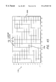
- FIG. 45 shows the core space 1230 being partitioned into a grid of twelve rows by twelve columns containing 144 elementary regions 1250 .
- R i,j each of the elementary regions, or regions, will be referred to as R 5,6 and region 1250 b , R 12,7 .
- FIG. 46 shows the relationship between the regions and the portions of the core space. As the table illustrates, in contrast to the one-to-one relationship between functions and portions, there is a one-to-many relationship between portions and the regions.
- the region is assigned to all of the portions which have its border within the region. For instance, as illustrated by FIGS. 44, 46 , and 47 , and by Table 3B(2) below, R 5,6 is assigned to portions 32 (f 1 ), 34 (f 2 ), 38 (f 4 ), and 42 (f 6 ). Table 3B(2) below partially lists the functions of the integrated circuit, the portions assigned to the listed function, and the regions assigned to the listed portions.
- Step Three Define the Pieces.
- the elementary regions 1250 are grouped into pieces, each piece being defined as a set of regions 1250 assigned to the same function or the same set of functions.
- a piece of the IC comprises a set of adjacent regions as illustrated by the figures of this specification; however, adjacency of the regions is not required to define a piece.
- FIG. 47 illustrates the relationship between the pieces and the regions of the core space
- Table 3B(3) below partially lists the pieces of the core space and the regions comprising each of the listed pieces.
- FIG. 48 shows all of the pieces of the integrated circuit 1230 for the example illustrated by FIGS. 44-47. For clarity of discussion, the pieces are referred to Pnnnn where nnnn is the reference number of the piece as illustrated by FIG. 48 .
- I(f) set of all pieces from which the portion of the core assigned to function ⁇ may take some space.
- I ⁇ P 1262 , P 1264 , P 1266 , P 1268 , P 1270 , P 1272 , P 1274 , P 1276 , P 1277 , P 1278 , P 1280 , P 1282 , P 1284 , P 1286 , P 1288 , P 1290 , P 1292 , P 1294 , P 1296 ⁇ .
- piece 12 P 62 comprises all elementary regions belonging to f 1 only.
- Piece 1264 comprises elementary regions each of which belongs to both f 1 and f 2 . Note that a piece can comprise only a single elementary region. For instance, piece P 1272 comprises only one elementary region R 5,6 which belong to functions f 1 , f 2 , f 4 , and f 6 .
- Each of the pieces has a capacity, or a maximum number of cells which can be placed in the core space defined by the piece. If a piece is assigned to a single portion (assigned to a function) of the core space, then entire capacity of the piece is available to the portion (i.e., to accommodate the cells of the function assigned to that portion); however, a piece, such as P 1270 , can be assigned to two or more portions, each portion representing a function. In such a case, the capacity of the piece is divided and allocated to the functions to which the piece belongs. Therefore, the following notation is used to express the capacity of a piece assigned to a portion, which, in turn, is assigned to a function:
- Step Four Define Capacity and Utilization Requirements
- a cell placement is acceptable when the placement results in a predetermined level of utilization for each of the portions assigned to the functions of the circuit.
- the cells are given fictive heights prior to being placed on the core space.
- the fictive height of a cell is the height of the cell used to calculate the space, or the number of cell height units, required to place the cell on the core space.
- the actual height of a cell is usually measured in millimicrons. Because all of the standard cells have the same width, the cell height is usually used as the measure of capacity as well has the height of the cell.
- the cells of the function should be placed on the core space such that the cells actually use fifty percent of the space provided for the cells on the core space. That is, when the cells of the function are placed on the core space, the ratio between the actual amount of the capacity used by the cells divided by the amount of the capacity taken up by or reserved for the cells must be fifty percent. Alternatively expressed, the utilization ratio determines the density of the space taken up to place the cells of the function.
- hh(f) the sum of all fictive heights of all cells of the function f.
- cap(P) the capacity of the piece P.
- cap(P) sum of all X f,P where P is a member of I(f), for all P's of the circuit;
- cap(P) is less than the sum of all X f,P for any of the pieces, then the capacity of the P, cap(P), is over-allocated, and the placement of the core space is not possible. To remedy the situation, the capacities of the pieces must be reallocated to the functions. On the other hand, if cap(P) is greater than the sum of all X f,P for any of the pieces, then the capacity of P, cap(P), is under-allocated, meaning that some core space of the piece is not allocated to any of the functions.
- Expression (B) states that, for each function, the sum of the fictive heights of all the cells of the function must be less than or equal to the sum of the capacities the function is assigned in each of the piece in which the function is assigned capacities. For example, referring to FIGS. 46 and 48, the sum of the fictive heights of all of the cells of f 1 (assigned to portion 1232 , which comprises P 1262 , P 1264 , P 1270 , and P 1272 ) must be less than or equal to the sum of the capacities of f 1 in P 1262 , P 1264 , P 1270 , and P 1272 . That is,
- Expression (A) if Expression (A) is not satisfied, then a solution is not feasible.
- the functions must be reassigned to different portions of the core space, the pieces may be redefined, or the capacities of the pieces may be reallocated to the functions until Expression (A) is met.
- Expression (B) is analyzed. If Expression (B) is met for a given cell placement, then the placement is a correct, and the processing stops. If Expression (B) is not met, then the following steps, Step Five, Step Six, and Step Seven, are followed to shift, or reallocate, the capacities of the pieces to meet Expression (B).
- Step Five Construct the Graph.
- a graph 1300 is constructed where each of the vertices of the graph corresponds to a function, and each of the edges connecting the vertices represents the pieces which contain borders or overlapping areas of the functions (vertices) which it connects.
- the vertices ( 1302 , 1304 , 1306 , 1308 , 1310 , 1312 , 1314 , and 1316 ) of the graph 1300 correspond to functions f 1 , f 2 , f 3 , f 4 , f 5 , f 6 , f 7 , and f 8 , respectively.
- Vertices are connected (by an edge) if the corresponding functions share at least one piece of the core.
- each of the dashed lines of the figure indicates multiple edges connecting the vertices while each of the solid lines indicates a single connection between the vertices.
- dashed-line edges 1302 a , 1302 b , and 1302 c indicate that f 1 (represented by vertex 1302 ) shares at least one piece with each of the functions f 2 (vertex 1304 ), f 4 (vertex 1308 ), and f 6 (vertex 1312 ), respectively.
- the dashed-line edges 1314 a and 1314 b indicate that f 7 (represented by vertex 1314 ) shares at least one piece of the core with functions f 6 (vertex 1312 ) and f 8 (vertex 1316 ), respectively.
- the solid-line edges 1304 a and 1306 a show that functions f 2 (vertex 1304 ) and f 3 (vertex 1306 ) share piece P 1268 (see FIGS. 47 and 48) of the core.
- Two different edges are used to indicate sharing of one piece of the core between two functions (vertices).
- the first edge represents the capacity of the shared piece assigned to the first vertex (function), which is potentially available to the second vertex (function).
- the second edge represents the capacity of the shared piece assigned to the second vertex (function), which is potentially available to the first vertex (function).
- edge 1304 a represents X f2,P1268 (the capacity of P 1268 assigned to f 2 ).
- the same capacity, X f2,P1268 is also the maximum amount of capacity f 2 may given up within P 1268 if f 2 is found to have excess capacity.
- the direction of the arrow of edge 1304 a indicates the direction in which the capacity may be reallocated, or shifted.
- Edge 1304 a is denoted as W(f 3 ,f 2 ,P 1268 ), and has the value X f2,P1268 .
- the edge 1306 a denoted W(f 2 ,f 3 ,P 1268 )
- has the value X f3,P1268 and represents the capacity of piece 1268 assigned to f 3 (vertex 1306 ), which is potentially available to f 2 (vertex 1304 ).
- vertices 1308 and 1310 (representing f 4 and f 5 , respectively) have two pairs of edges ( 1308 a , 1310 a and 1308 b , 1310 b ) connecting them because f 4 and f 5 share two different pieces, P 1282 and P 1284 .
- the value of the edges are:
- edge 1308 a denoted W(f 5 ,f 4 ,P 1282 ), has the value X f4,P1282 ;
- edge 1310 a denoted W(f 4 ,f 5 ,P 1282 ), has the value X f5,P1282 ;
- edge 1308 b denoted W(f 5 ,f 4 ,P 1284 ), has the value X f4,P1284 ;
- edge 1310 b denoted W(f 4 ,f 5 ,P 1284 ), has the value X f5,P1284 .
- Step Six Identify the Functions with Capacity Shortages and the Functions with Excess Capacity.
- each of the vertices (functions) are analyzed and grouped into two sets of vertices V 1 and V 2 . All functions (vertices) with deficiencies of capacity are assigned to group V 1 . All functions with a shortage of the core space satisfy the expression:
- hh(f) >the sum of the capacities of all pieces which contribute core space to the function (i.e., the sum of all X f,P for all P belonging to I(f)).
- V 1 contains all vertices (functions) which do not have sufficient core space to place all of their cells.
- V 2 The functions (vertices) with excess core space are assigned to V 2 . All functions with excess core space satisfy the expression:
- V 2 contains all vertices (functions) which have more than the core space needed to place their cells.
- Step Seven Shifting Excess Capacities to Meet Deficiencies.
- the graph 1300 is traversed until a vertex belonging to V 2 is encountered.
- the traversal is in the opposite direction of the arrows of the FIGS. 49 and 50 because the direction of the arrow indicates the direction in which the excess capacities can be shifted.
- the chain begins with a first vertex (function, f first ) in V 1 and ends in a second vertex (function, f second ) in V 2 .
- the maximum capacity that can be shifted from f second to f first , ⁇ is the smallest of the following three values:
- the capacities of the each pieces of the chain is updated as to shift the amount of capacity, represented by ⁇ , from the second vertex (f second ) to the first (f first ) vertex by updating the edge values of each of the edges of the chain.
- FIG. 50 The process can best be illustrated using an example shown by FIG. 50 .
- FIG. 50 Referring primarily to FIG. 50, but also to FIGS. 44-48, the following facts are assumed for this illustration:
- the vertices have the following properties:
- vertex 1306 (representing f 3 and belonging to set V 1 ) is deficient by 500 cell height units.
- hh(f 3 )>X f3,P1268 and hh(f 3 ) ⁇ X f3,P1268 500 cell height units;
- vertex 1302 (f 1 , set V 2 ) has 300 excess capacity
- vertex 1310 (f 5 , V 2 ) has 1200 excess capacity
- vertices 1304 (f 2 ) and 108 (f 4 ) have no deficiencies or excess capacities.
- edges have the following properties:
- the 500 cell height unit deficiency of f 3 can be remedied by shifting the capacities along the following two chains of the graph 1320 .
- the 300 excess capacity of f 1 (vertex 1302 ) can be shifted to f 3 (vertex 1306 ) via piece 1264 (edge 1302 b ), f 2 (vertex 1304 ), and piece 1268 (edge 1304 a ).
- the chain can be denoted 1302 ⁇ 1302 b ⁇ 1304 ⁇ 1304 a ⁇ 1306 .
- the maximum capacity of the chain, ⁇ is the minimum of the following three numbers:
- the 200 units of 1200 excess capacity of function f 5 can be shifted to f 3 in a similar operation using Chain 2 which can be denoted 1310 ⁇ 1310 a ⁇ 1308 ⁇ 1308 c ⁇ 1304 - 1304 a ⁇ 1306 .
- the maximum capacity, ⁇ , of Chain 2 is 200, the lowest maximum edge capacity of all of the edges of the chain, which, in this case, is from edge 1308 c.
- the physical area assigned to the neighboring functions can be increased;
- elementary region grid can be modified to create shared core space pieces encompassing the function and its neighboring functions.
- a one dimensional iterative optimization initially provides a fast, good cell coordinate placement.
- the one dimensional iterative optimization is performed in both the x and y directions.
- the iterative optimization may be performed in the y direction initially, but the preferred method is to perform it in the x direction.
- a netlist or hypergraph H includes the set V of cells v and the set Q of nets q.
- x or “X” is used below for calculation in the x-direction
- y or “Y” would be used.
- “z” and “Z” are universal notations representing either “x” and “X”, on the one hand, or “y” and “Y” on the other, depending on which direction is being considered.
- FIG. 9 illustrates a cell v 102 having several pins which belong to the net q 104 .
- the origin 106 of the cell defines the default “position” of the cell. If a net q 104 is being evaluated by the system, then the pin 108 on the cell v 102 which is on the net q 104 is positionally defined relative to the origin 106 . Any point may be defmed as the origin of the cell, including its center of mass, but the preferred embodiment is to define the origin at the physical lower left corner of the cell as shown in FIG. 9 .
- the core 201 is divided into subregions R. Initially, the preferred value of R is one, indicating the core is not subdivided.
- the subdivision of the core is represented by an array X[i] of x-coordinates of vertical dividing lines 202 ( 1 ) through 202 ( n ) and an array Y[j] of y-coordinates of horizontal dividing lines.
- X[i] and X[i+1] For each interval X[i] and X[i+1], a dividing point is calculated to determine fmer resolution.
- Each cell v belongs to some of these intervals, and the interval function I[v] is equal to i if the cell v belongs to the interval X[i], X[i+1].
- the current coordinates of the cell v are denoted as Z[v], while the coordinates of the net q are denoted by Z[q].
- each movable cell coordinate is assigned a coordinate of a dividing point of the interval the cell occupies.
- Z[v] DX[I[v]].
- DX is typically the midpoint of the interval, but the dividing point may be at a different location in each interval while still within the scope of the current invention.
- the movable cell coordinate 203 is located at the dividing point 204 of the interval, which is a point at a percentage of the width or length of the core region 201 .
- the preferred implementation is locating the dividing point 204 at the center point of the surface abstraction of the core region.
- Fixed cells are assigned their real coordinates.
- the flowchart of FIG. 12 demonstrates the procedure for obtaining an initial one dimensional placement of the movable cells.
- the movable cells are assigned the coordinate of the center of the region where they are located in initialization step 250 .
- the new cell coordinate Z[v] is equal to: ⁇ ⁇ [ v ] * ⁇ ⁇ 1 ⁇ q ⁇ ⁇ Z * ⁇ ( q , i )
- Z* (q,i) is calculated by determining a temporary value a, where a initially equals Z[q]. If a is greater than X[i+1], or is outside the interval, then a is set to the greater border condition, or equal to X[i+1]. If a is less than X[i], again outside the interval, then a is set to the lesser border condition X[i]. Finally, Z* (q,i) is set equal to a.
- This set of steps places the coordinates of the nets along an imaginary line as shown in FIG. 13, line 225 .
- Cells are placed along this line based on the results of the initial Z(v) calculation described above, and these positions are subsequently iteratively moved to new positions in the region.
- the positions of cells within the region are shown in FIG. 14, which includes positions where some of the nets are initially outside the region. These out of bounds nets are then set to the edge of the region.
- the difference between the previous value of the cost function and the new value of the cost function is determined in step 253 .
- the typical cost function used is wire length and the cost function is computed as the average of the half-perimeters of boundary boxes for all nets.
- the typical cost function used is wire length and the cost function is computed as the average of the half-perimeters of boundary boxes for all nets.
- This difference is evaluated in step 254 , and if the difference is not below a predetermined threshold, the cell positions are iterated by repeating net coordinate computation step 251 and new cell coordinate computation step 252 .
- This iteration procedure is repeated for a number of times, such as one hundred times, or until the difference in cost function of two consecutive iterations is less than a predetermined threshold, such as 0.001 microns.
- a predetermined threshold such as 0.001 microns.
- a unit may be any measure, but the preferred distance threshold is 0.001 microns. The number of iterations and the threshold may vary while still within the scope of the invention.
- Section 5 Fast Procedure for Finding a Levelizing Cut Point
- the surface abstraction, or core region 201 denotes a region R[i,j].
- the previous one dimensional fast preplacement procedure provides a given dividing point DX[i], if the region is divided horizontally, or DY[j] if the region is divided vertically. This dividing point may be anywhere along the line containing the cells from the previous procedure, but the preferred location is the midpoint of the line.
- the dividing point in the current example generates two subregions in the region R[i,j].
- the placement of nets along the line in the x direction is partitioned along a dividing line 300 providing two subregions containing the cell positions.
- the capacity of each of these regions is the area of the regions without all fixed cells or blockages.
- the capacities of the two regions are cap 0 and cap 1 .
- a cut point, Z 0 is desired which divides the cells such that a percentage of cells or cell heights is proportional to the size of the region. For example, if a 50% cut point is desired, the required location for the cut point is where the two regions, defined by the physical 50% border dividing the surface abstraction, would have equal numbers of cells or of cell heights. As shown in FIG.
- a region physically divided in half by a dividing point 300 may not have a cut point and cut line 301 coexistent with the region dividing point.
- the sum of all heights of all cells having coordinates lower than Z 0 , or of the total quantity of cells having coordinates lower than Z 0 must not be greater than cap0 cap0 + cap1
- Initialization step 326 initializes an array S[k] having N elements, stores the sum of heights of all cells having subintervals with indices less than or equal to k, and initializes all the elements of array S[k] with the value zero.
- (A,B) is an interval from 0 to 200 and 10 equal subintervals are desired. In fact, a number in the range of 1000 such intervals would normally be desired, but 10 is used here for purposes of illustration. Further, assume that one cell is located in each of the ten subintervals, as shown in FIG. 17, although it would be probable that subintervals would contain more than one cell. Assigning A has a value of zero, and B a value of 200, n(v) for a cell in this arrangement is equal to the minimum integer value greater than Z(v)/10 for the cell.
- the designation “]x[” denotes take the minimum integer greater than x, such that for x having a value of 1.3, the value of ]x[ is 2.
- Height accumulation step 328 accumulates the heights of the cells in each subinterval within the array S[k] according to the relationship:
- step 329 calculates the values within S[k] by iterating for k equal to 2, k being less than or equal to N, incrementing k,
- Cut point index locator step 330 locates the minimal index k 0 such that cap0 cap0 + cap1 * S ⁇ [ N ] ⁇ S ⁇ [ k 0 ]
- Clustering of cells within a single region, or at a border of a region, may provide an inaccurate cut point.
- the subinterval where the levelizing cutpoint is located may be again divided into N subintervals in subdivision step 332 and the procedure repeated, locating a second levelizing cutpoint.
- the levelizing cut point Z 0 divides the cloud of cells proportionally to the capacities of the subregions induced by the dividing point D.
- offset calculation step 350 determines the offset of the cut line from the dividing line, where ⁇ is the difference between the coordinates of dividing point D and the levelizing cut point Z 0 . Coordinates for each cell in the region are modified such that for any cell v within the region R[i,j], the cloud of cells is shifted in shifting step 351 such that the cut point is collocated with the dividing point:
- a is greater than X[I[v]+1] then a is equal to X[I[v]+1]. If X is less than X[i[v]], then is equal to X[I[v]]. Z[v] is then set equal to this value a.
- the system initially places all cells at the center of the two-dimensional abstraction of the chip surface.
- the system then performs a predetermined number of iterations of the One Dimensional Preplacement Optimization in one direction, such as the x direction.
- the surface abstraction is then subdivided into sub-regions by dividing the surface abstraction in the opposite direction.
- the system uses the Levelizing Cut Point procedure to partition the cells into groups proportional to the capacities of the subregions.
- the Median Control procedure modifies the coordinates of the cells.
- the Levelizing Cut Point and Median Control procedures are iterated a specified number of times (preferably 6) with the specified number of iterations comprising a Block.
- the average cost function is computed after a Block is performed.
- an overall cost function is computed. After repeating this Block a predetermined number of times (typically 10), the system computes the average cost of each cost calculated during these Block iterations. The current average cost value is compared with the previous average cost value, and if the difference between the average value and the previous value is less than a predetermined value (such as 10 ⁇ 3 ), the procedure for the first level of hierarchy is complete. Cells are then assigned to the respective subregions depending on the calculated coordinates.
- the system may repeat the aforementioned procedures based on a cut in the opposite direction. If, for example, the initial iterative one-dimensional preplacement optimization divides the available space on the surface abstraction by a vertical line, or divides in the x direction, the system executes the finding of a levelizing cut point procedure and the median control and resolution increase procedure in this direction. Upon completion of these procedures, the cells are assigned to one of the two regions, and the procedure may be repeated in the y-direction, based on the cells located in the two regions, after other optimization procedures discussed below are completed. As shown in FIG. 20, the two regions are divided using two dividing lines in the y direction and cells are placed along these two lines. The system locates a levelizing cut point for each region and partitions out the cells to the four remaining cells. This division in the y direction creates a second level of hierarchy.
- hierarchy levels are determined based on the number of divisions of the surface abstraction.
- the level of hierarchy is the sum of the number of times the surface abstraction is divided into separate regions. For example, if the surface abstraction has been divided three times in the x direction and two times in the y direction, the system has reached the fifth level of hierarchy.
- the total number of regions is equal to 2 (Levelx+Levely) , with “Levelx” meaning the number of occasions that the surface abstraction has been divided in the x direction and “Levely” means the number of occasions that the surface abstraction has been divided in the y direction.
- 32 regions exist at the fifth level of hierarchy.
- the system After each surface abstraction division, the system performs a discrete placement optimization. For purposes of illustrating this procedure, it is assumed that the previous routines have furnished two sets of cells partitioned into two regions on the surface abstraction. All cells are located in the centers of each region.
- the system calculates affinities and cost functions for the arrangement.
- An affinity is calculated based on current cell placement and blockages in a chip. Affinities are heuristically connected with a desired cost function, which should be minimized. Affinities can be driven by cell density, wire length, minimizing maximal cut, clustering, etc., or some combination of these parameters depending on the goal sought to be achieved. Affinities may be positive or negative, and relate to the quality of an alternate placement of a cell. For example, having a cell with a higher affinity at a first location and a lower affinity at a second location indicates that the preferred placement of the cell is the first location.
- the parameter of the discrete placement optimization is ⁇ , which represents the accuracy of the placement, and is a small number, such as 10 ⁇ 3 or 10 ⁇ 4 .
- adjacent cell location step 400 initially considers moving a cell from its current position to each of the adjacent regions, as well as considering leaving the cell in the current region. For higher levels of hierarchy (i.e., a substantial number of regions), nine total regions are evaluated for cells not located on an edge of the surface abstraction.
- Affinity calculation step 401 calculates, for each adjacent region, the maximum affinity of the cell is moved to these adjacent regions.
- the total number of cells having an affinity greater than a predetermined value p is denoted N p .
- the affinities for the cells are calculated and ordered according to these affinities.
- Global threshold evaluation step 402 finds a threshold number, Globthresh, such that the total number of cells, N GlobThresh , having an affinity greater than the threshold number, is less than ⁇ multiplied by the number of all cells having positive affinities, or N 0 .
- ⁇ having a value of from 30 to 40 per cent.
- the overall global threshold is determined using a similar procedure to that described above with reference to the procedure for finding the levelizing cut point.
- the affinities are ordered sequentially, and all cells are defined to be within an interval (A,B), exclusive of negative affinities.
- the (A,B) interval is subdivided into k equal subintervals in subdivision step 450.
- Initialization step 451 defines an affinity array A[i] having i elements. The initial value of all elements of this array is 0.
- A[i] stores the number of cells whose affinities are greater than or equal to (k ⁇ i)*L, where L is the length of the subinterval within (A,B).
- calculation step 452 computes an index i(v) of the subinterval where the cell v affinity is located:
- Cell affinity summation array step 453 calculates the value of A[i] by iterating for i equal to 2, i being less than or equal to k, incrementing i,
- Global affinity evaluation step 454 determines the global affinity threshold GlobThresh using the previous equation such that GlobThresh is equal to i where i is the minimum i such that N 0 ⁇ is less than or equal to A[i].
- Affinity comparison step 455 calculates the maximal affinity for the present region and for each adjacent region. If the affinity for an adjacent region is greater than the global threshold GlobThresh, the cell is placed in the new region in cell repositioning step 456 . The original cell position data structure is updated in data structure update step 457 . Then steps 455 , 456 and 457 are iterated as a block 458 , generally 3 times.
- the result of this procedure is a global threshold for all cells. Some cells have been moved to adjacent regions, altering affinities of other cells. The procedure is then repeated two more times, for a total of three iterations, through the list of all movable cells using the same threshold.
- a local threshold can be calculated in addition to the global threshold.
- the local threshold is calculated in the same fashion as the global threshold, but with respect to only the cells from the region where the cell is located. If we use this additional, optional procedure, we move the cell only if the maximal affinity is greater than both the global threshold and the local threshold.
- An average cost function representing the average of the three values of the cost function calculated after each iteration, is computed. Now we compute a new threshold as described above in step 454 . This entire procedure, from threshold computation through cost function computation (block 459 ), is repeated a predetermined number of times (usually 10 times). Each time block 459 is repeated the predetermined number of times, the average value of the average cost function is calculated and compared with the previous average value of the average cost function value. If
- ⁇ is a small number, typically 10 ⁇ 3 or 10 ⁇ 4 .
- the surface abstraction is partitioned alternately in the vertical and horizontal directions, where each division denotes an additional level of hierarchy.
- the levels of hierarchy, Lev x and Lev y determine the number of hierarchy levels.
- the number of grids, or channels of regions, in each direction are given as Grid x , equal to 2 Levx , and Grid Y , equal to 2 Levy .
- Each region on each level of hierarchy is determined by (Lev x , Lev y , i, j) where i and j are the indices of corresponding surface abstraction segments.
- the capacity of each region is a function of these four parameters. The system then calculates the sum of the heights in each region.
- the system calculates a region capacity in terms of the heights of cells which can be located within a single region.
- This capacity of cell heights accounts for rows or columns of locations where cells may be located. As shown in FIG. 23, the cell region will have a certain number of columns, or possibly rows, located therein.
- the cell height capacity represents the space available to individual cells within the region and is based on the hierarchy of the surface abstraction. As outlined below, the highest level of hierarchy defines a single column per region. As may be appreciated by one of ordinary skill in the art, rows may be used rather than columns to define a total cell width capacity rather than a height capacity.
- All cells are located at the center of a region during some phases of the placement procedure.
- the height of a single cell may extend into more than one region.
- a parameter ColKey is assigned to this placement system process.
- the center of each cell is assigned to the center of the region it occupies. If ColKey has a value of 0, the entire height of the cell is located within a single region. If ColKey is equal to 1, the height of the cell is distributed to the regions the cell overlaps. For example, if a cell has a height of 16 units while the region has a height of ten units, three units are assigned to the cell above and three to the cell below the current cell.
- Cells located in an edge region are assigned to the region away from the edge, and not to any region outside the edge. Hence in the example previously presented, ten units of the cell would be assigned to the edge region and three to the region above the edge region.
- Movement of the cells from one region to another requires updating the total of the heights in each region.
- Each cell v is located within regions with indices I[v] and J[v], in the x and y directions, respectively. Movement of a cell to an adjacent region is denoted by ⁇ i and ⁇ j , where ⁇ i is a movement in the horizontal direction, with a rightward movement being +1, and ⁇ j representing vertical movement, upward yielding a +1 value. ⁇ i and ⁇ j each are set at either ⁇ 1, 0 or +1. From FIG.
- penalty calculation step 501 computes a penalty, PenCapB(v, ⁇ , ⁇ i , ⁇ j ), equal to the following values: SumHeight ⁇ [ I ⁇ [ v ] ] ⁇ [ J ⁇ [ v ] ] Cap ⁇ [ I ⁇ [ v ] ] ⁇ [ J ⁇ [ v ] ] * 2 k
- ⁇ i and ⁇ j have a value other than 0 ( ⁇ 1 or +1)).
- ⁇ represents the degree of counting, which affects the movability of a cell v to a new region. ⁇ will typically have a value between 0.1 and 1.
- Prior level calculation step 502 computes the penalty for the regions three levels before the current level. For example, if the current hierarchy divides the surface abstraction into 64 by 64 total regions, then three levels before has 8 by 8 regions. A total of 64 eight by eight regions will fit into a 64 by 64 area.
- the total penalty, PenCap8(v, ⁇ i , ⁇ j ) is calculated in the same manner as the PenCapB calculation in total penalty computation step 503 .
- the total capacity penalty is calculated in step 504 according to the following formula:
- PenCap(v, ⁇ i , ⁇ j ) ⁇ *PenCapB(v, ⁇ , ⁇ i , ⁇ j )+SW* ⁇ ad *PenCap8(v, ⁇ i , ⁇ j )+ColKey* ⁇ col *PenCapCol(v, ⁇ , ⁇ i , ⁇ j )
- ⁇ is the capacity penalty weight in the total affinity
- Sw is a switch parameter set to 0 or 1 depending on whether use of the PenCap8 variable is desired.
- PenCap8 is used only when the area is divided into 16 by 16 regions or more.
- ⁇ 0 ranges between 0.5 and 1.5
- CoreX is the x dimension of the core.
- the values initially selected for ⁇ col and ⁇ ad are 16 and 16.
- Section 9 Wire Length Driven Affinity System
- An alternate embodiment of the current design is to calculate affinities and penalties according to the relative wire lengths of different designs. This procedure provides a set of affinities providing the minimal wire length over all feasible placement solutions.
- X(w) is the current coordinate of the cell origin
- x(v,q) is a pin offset from the origin where the pin belongs to the net q.
- the y component penalties are similar:
- the penalty vector for the individual situation is as follows. If X max is less than X l , then the vector representation for the penalty in the x direction is ( ⁇ 1,0,1), indicating zero penalty for keeping the cell in its current location, a penalty of one for moving the cell to the right, and a penalty of ⁇ 1 for moving the cell to the left. This indicates that a cell in the net is outside the left boundary of the region, and movement of the entire net to the right would be a penalty for the wire length. Movement of the cell to the left would be a negative penalty, or benefit, to the wire length. For X min greater than X r , the penalty vector is (1,0, ⁇ 1).
- the penalty vector is (0,0,1). For X min less than X l and X max less than or equal to X r , the penalty vector is (0,0,1). For X min less than X l and X max greater than X r , the penalty vector is (0,0,0). For X min greater than or equal to X l and X max less than or equal to X r , the penalty vector is (1,0,1). For X min greater than or equal to X l and X max greater than X r , the penalty vector is (1,0,0). Similar vectors result for positions of the cells in the y direction.
- the total penalty for a cell v in the X direction is a normalized sum of the penalties in the X direction over all nets incident to the cell v:
- PenHP x ⁇ ( v , ⁇ i ) ( XI ⁇ [ 1 ] - XI ⁇ [ 0 ] ) * ⁇ q ⁇ v ⁇ ⁇ PenHP x ⁇ ( v , q , ⁇ i )
- PenHP Y ⁇ ( v , ⁇ j ) ( YJ ⁇ [ 1 ] - YJ ⁇ [ 0 ] ) * ⁇ q ⁇ v ⁇ ⁇ PenHP Y ⁇ ( v , q , ⁇ j )
- the total penalty is the sum of the x and y components:
- PenHP(v, ⁇ i , ⁇ j ) PenHP X (v, ⁇ i )+PenHP Y (v, ⁇ j )
- AffHP(v, ⁇ i , ⁇ j ) ⁇ PenHP(v, ⁇ i , ⁇ j )
- Aff(v, ⁇ i , ⁇ j ) AffHP(v, ⁇ i , ⁇ j )+QEF(v)*AffCap(v, ⁇ i , ⁇ j )
- Height(v) represents the height of the cell v. Although any values may be used for A and B in this equation, experience and testing has shown that the values of 5 and 5 produce the most beneficial results.
- Another parameter used to produce an affinity for improving cell placement is minimizing the maximal number of nets that intersect the unit segment of the grid system imposed of the surface abstraction of the chip. Net overlap inherently yields inefficiency of wiring, and thus minimizing the number of nets which cross other nets improves overall system efficiency.
- the number and position of the vertical and horizontal lines which induced the level of partitioning hierarchy are evaluated, including determining the number of nets which intersect a line partitioning the cell into regions. Initially, the system determines the number of nets which intersect the lines and the relative affinities for these line crossings. The system moves the cells and the nets change position based on relative affinities, and then the number of net crossings and affinities are recomputed.
- each dividing line partitions regions, and each of these regions has a capacity denoting the volume of cells which can fit within the region.
- the system performs the following procedure once after each bisection.
- the system calculates the capacities as an average capacity of regions adjacent to the dividing line.
- the capacity of dividing line X(i) is defined as the average capacity of all regions to the left of the line and all regions to the right of the line.
- the system calculates average vertical line capacity and average horizontal line capacity for all lines, representing the amount of wiring which is available over the entire surface abstraction.
- the capacity may also represent available space for wiring available on multiple layers of the chip.
- the capacity of each horizontal and vertical line is then divided by the corresponding horizontal or vertical average values.
- the relative cut of the line is 1.5.
- the ratio of the number of nets crossing a line and the capacity of the line are defined as the relative cut.
- the system calculates a midcut for the surface abstraction.
- the midcut represents the average relative cut over all lines of the surface abstraction.
- FIG. 27 represents a region having indices (TX, TY).
- the number of cuts represents, with the current cell configuration, the number of times a net crosses a boundary, while the capacity of the line represents the total number of possible crossings of the particular boundary.
- the system calculates four penalties which represent the cost of a change for a half-perimeter move of cells within the region one unit to the right, left, up, and down:
- DXL ⁇ ( XI ⁇ [ 1 ] - XI ⁇ [ 0 ] ) * ( 1 - ⁇ + ⁇ * ( CutX ⁇ [ TX ] CapX ⁇ [ TX ] / ( MidCut ) )
- DXR ⁇ ( XI ⁇ [ 1 ] - XI ⁇ [ 0 ] ) * ( 1 - ⁇ + ⁇ * ( CutX ⁇ [ TX + 1 ] CapX ⁇ [ TX + 1 ] / ( MidCut ) )
- DYB ⁇ ( YJ ⁇ [ 1 ] - YJ ⁇ [ 0 ] ) * ( 1 - ⁇ + ⁇ * ( CutY ⁇ [ TY ] CapY ⁇ [ TY ] / ( MidCut
- Discrete affinities in the x and y direction represent the numbers of nets whose half-perimeter decreases on movement of cells across the boundary minus the number of nets whose halfperimeter increases when a cell moves in a given direction.
- Affinity for zero movement represents the numbers calculated above. Movement of a cell in a particular direction, such as crossing a boundary line, induces an affinity for that cell. From FIG. 27, movement of the cell to the right and up decreases the penalty, or increases the affinity for the cell. Thus affinity in the x direction, AffX, for movement to the right is ⁇ 1, to the left is 1, and affinity for movement in the y direction, AffY for movement of the cell upward is ⁇ 1, and downward is 1. Affinity for keeping the cell in its current position is 0.
- Total affinities for movement of the cell in the vertical and horizontal directions are the summation of affinities in the X and Y directions:
- Each moveable cell v is located within a neighborhood Neigh(v) constructed in accordance with the optimization of cell neighborhood system procedure outlined above. That procedure yields an ordering of cells according to the cells' distance from the center of the neighborhood, after optimization.
- weight assignment step 601 assigns each cell a weight equal to the size of the neighborhood M minus the index of the cell i. Thus, for a neighborhood of size 20, the 20th cell has a weight of 0, while the first cell has a weight of 19.
- An alternate preferred method of assigning weights is to declare a number L, where L equals M plus some positive integer, such as 2, and weights range from 21 down to 2. The reason for this shift is that the weight accorded to a factor of 1 is infinitely greater in terms of multiplications than a factor of zero. Thus relative weights may be misleading if low number factors, such as zero and one, are used as weighing factors. Any monotonically decreasing function may be employed in defining the weights accorded the cells within the neighborhood.
- the system then calculates attraction weights in step 602 .
- affinity definition step 603 the system then defmes the following neighborhood affinities for movement of cells in each particular direction:
- AffNeighborhood x ⁇ ( v , - 1 ) 2 * Grid Y Grid X + Grid Y * 1 M 2 * ( SumWeight l ⁇ ( v ) - SumWeight o ⁇ ( v ) - SumWeight r ⁇ ( v ) )
- AffNeighborhood x ⁇ ( v , 1 ) 2 * Grid Y Grid X + Grid Y * 1 M 2 * ( SumWeight r ⁇ ( v ) - SumWeight o ⁇ ( v ) - SumWeight l ⁇ ( v ) )
- Grid X and Grid Y are identical to the values outlined above in reference to the density driven capacity penalty system, and represent the number of grids, or lines of regions, in the X and Y directions.
- Grid X is equal to 2 Levx and Grid Y is equal to 2 Levy where Lev x and Lev y define the number of hierarchy levels.
- the number M represents the number of cells in the neighborhood.
- M is equal to five and we are in the fourth level of hierarchy.
- AffNeighborhood X (v,0) equals 0, and AffNeighborhood X (v, ⁇ 1) equals (2*2/(2+2))*1/5 2 *(17 ⁇ 5 ⁇ 3), or 9/25.
- AffNeighborhood X (v,1) equals (2*2/(2+2))*1/5 2 *(3 ⁇ 5 ⁇ 17), or ⁇ 19/25.
- the X affinities for this example are (9/25, 0, ⁇ 19/25) for leftward, center, and rightward movement, respectively.
- the Y affinities for this example are ( ⁇ 17/25, 0, and ⁇ 15/25).
- Combinations of capacity affinities, wire length affinities, cut affinities, and neighborhood affinities present an enhanced system of determining the preferred direction of movement of a cell or net.
- Such an affinity combination may include combining the following affinities:
- Aff(v, ⁇ i , ⁇ j ) AffNeighborhood(v, ⁇ i , ⁇ j )+QEF(v)*AffCap(v, ⁇ i , ⁇ j )
- QEF(v) represents the capacity penalty influence factor, which is a function of cell v relative height.
- Such a combination of affinities takes into account cell position as well as relative weight accorded to an individual neighborhood.
- the combination of affinities introduces an element of randomization.
- a deterministic system for combining affinities which converges at a relatively rapid rate is desired to optimally utilize affinities.
- Such a system which iteratively optimizes cell placement using a combination of affinities is the functional sieve approach.
- the functional sieve performs several calculated iterations of combining affinities and moving cells based on relative affinities and then computing cost functions for the new cell positions.
- the functional sieve utilizes the following basic formula:
- Aff(v, ⁇ i , ⁇ j ) ⁇ 1 *AffNeighborhood(v, ⁇ i , ⁇ j )+ ⁇ 2 *AffHP(v, ⁇ i , ⁇ j )+QEF(v)*AffCap(v, ⁇ i , ⁇ j )
- the system in step 651 iterates a predetermined number of times, preferably once, calculating the above affinities with ⁇ 1 equal to one and ⁇ 2 equal to zero.
- This iterative procedure produces affinities and cells which are then repositioned based on the combined neighborhood and capacity affinities.
- the system in step 652 performs a predetermined number of optimization iterations with ⁇ 1 equal to zero and ⁇ 2 equal to one, moving the cells based on cut and capacity affinities.
- the first iterative procedure involving neighborhood and capacity affinities combined with the second iterative procedure entailing cut and capacity affinities define a major iteration.
- the system in step 653 calculates the value of the cost function.
- the preferred cost function is wire length.
- the system After computing the cost function, the system performs a predetermined number of major iterations and calculates the cost function after each major iteration.
- the preferred number of major iterations and cost function calculations is six.
- the system computes the average cost value for all of the costs calculated in the previous steps. This procedure steps through different affinity evaluations and obtains a preferred overall movement of cells on the surface abstraction. The functional sieve optimization process is halted when two consecutive cost average function values satisfy a given accuracy, such as 10 ⁇ 3 or 10 ⁇ 4 .
- the ⁇ 1 parameter is utilized in a larger number of iterations than the ⁇ 2 parameter. Subsequently, the system performs several iterations with ⁇ 1 equal to zero. The entire block is iterated a predetermined number of times in this discrete placement procedure, typically three to five times.
- a crystallization procedure produces fine placement of the cells after the aforementioned functional sieve procedure is completed.
- the system uses a small non-zero value, such as 10 ⁇ 2 , for ⁇ 1 a predetermined number of times, such as once, in the major iteration and the zero value several times. This procedure produces a detailed placement of cells.
- An alternate embodiment of the current functional sieve alters the multiplying factors for the various affinities. Such an embodiment is particularly useful in crowded net situations, and emphasizes cross cuts while taking advantage of open nets.
- Aff(v, ⁇ i , ⁇ j ) ⁇ 1 *AffNeighborhood(v, ⁇ i , ⁇ j )+ ⁇ 2 * [(1 ⁇ )*AffHP(v, ⁇ i , ⁇ j )+ ⁇ *AffCut(v, ⁇ i , ⁇ j )]+QEF(v)*AffCap(v, ⁇ i , ⁇ j )
- ⁇ is a number between zero and one, depending on the emphasis desired placed on the number of cuts.
- affinity combinations disclosed within this functional sieve operation are not limited to those disclosed here, and may include other combinations using other weighing factors. Such an alternate weighing and affinity scheme would produce a desirable placement of cells and still within the scope of the present invention.
- a coarse overflow remover procedure is applied on the highest level of the chip core region hierarchy when each region contains a piece of only one column.
- the list of cells is scanned in the order of decreasing heights in order to find a new region for each of them.
- a list of cells in order of decreasing cell height is made. If the height of a cell is smaller than the available space in the corresponding column segment, then the cell retains its location. Most of the cells will keep their previous positions if the initial cell density is acceptable.
- FIG. 33 represents a portion of the chip that has seven columns 800 - 806 .
- the cell columns 800 - 806 are partitioned into maximal segments without blockages.
- a plurality of megacells 810 may be located in the upper left corner.
- the megacells 810 are shown to extend across the columns 800 - 802 .
- a first blockage 830 extends across the second and third columns 801 and 802 , and a second blockage 832 extends across the column 806 .
- Column 800 has two adjacent regions 812 and 814 that are assigned to a single column segment 815 .
- Each of the column segments actually consists of a few regions, and each region belongs to exactly one of the segments. For each segment the total height of all cells assigned to the segment is retained.
- the column 806 segment includes a region 816 that has a cell height of twenty-two and an adjacent region 818 that has a cell height of six. Therefore, the column segment 806 includes a column segment 820 that has a cell height of twenty-eight. This process is applied only to cells that have been already scanned, i.e. in the beginning of the process all those sums are equal to 0.
- the capacity of a column segment is its height.
- the next cell from the list will get a new position according to the following rule: look for the closest (using Manhattan distance) region to the current cell so that the corresponding column segment will not have an overflow capacity if the next cell is assigned to that region.
- a preferred order for scanning the regions is shown in FIG. 34 . First consider the original region (marked with the numeral 0) and then consider the regions having a distance of 1, then consider the regions having a distance of 2, etc.
- This step considers only cells that already were assigned new positions and the current one. Usually, a cell is going to stay on the old position. As soon as the region is found that satisfies this condition, the region scanning is stopped, and assign the cell to that region. If the original region satisfies the condition, the cell is reassigned to the original region.
- FIG. 36 is a flow chart of an overlap remover according to the invention.
- the overlap remover process is applied separately to each column of cells. It is assumed that each column is continuously connected with no blockages between cells of the same column. As shown in FIG. 35, denote the top and bottom of the column with index j by T[j] and B[j], respectively. Similarly the top and bottom of column k are denoted by T[k] and B[k], respectively.
- the vertical grid step is used as the unit of measure.
- the parameter zaz is defined as the distance between the top of one cell in a column and the bottom of the next cell upward. There must be at least one grid space between adjacent cells to have a feasible layout.
- FIG. 37 illustrates a numerical example.
- the parameter minzaz satisfies the condition minzaz ⁇ ⁇ H col _ - H cell _ # ⁇ ⁇ cells + 1 .
- the parameter of the overlap remover process is integer values of minzaz, which can be positive or negative.
- the process further includes the step of modifying the array zaz such that all its elements are not less than minzaz.
- the array elements are processed forward and backward alternately. The following procedure is executed:
- FIG. 36 is a flowchart of a preferred process adjusting cell spacing in the column to remove overlap with minimal noise.
- a process step 908 compares zaz(i) a parameter maxzaz, where maxzaz is the largest value of zaz(i) that will be permitted on the chip. If zaz(i) is less than maxzaz and the count is greater than 0, then zaz(i) is replaced by zaz(i) plus one grid step (zaz(i) ⁇ zaz(i)+1) in a process step 910 . The counter is then decremented by one in a process step 912 , and the foregoing steps 902 , 908 , 910 and 912 are repeated until the count becomes zero.
- zaz(i) is not less than minzaz and the condition count>0 and zaz(i) ⁇ maxzaz is not satisfied.
- zaz(i) is compared to maxzaz. If zaz(i) is greater than maxzaz, then zaz(i) is replaced by maxzaz in a step 916 . The count then is incremented by the quantity [zaz(i)-maxzaz] in a step 918 .
- the steps 902 , 908 , 914 , 916 and 918 are repeated for the selected cell until the condition zaz(i)>maxzaz of step 914 is not satisfied.
- the result of adjusting the cell spacing in accordance with this preferred process is that overlap between cells is removed and spacing that were too large have been reduced to acceptable values.
- Cells that previously overlapped now have a spacing zaz(i) of one grid space.
- Cells that were too far apart now have spacings zaz(i) such that minzaz ⁇ zaz(i) ⁇ maxzaz.
- the ColKey parameter has been discussed above in the section that describes the density-driven capacity penalty system.
- the ColKey parameter should be set to 1. Setting the ColKey parameter to 1 means that the height of a cell is distributed over all regions with which the cell overlaps. Precisely, if the cell has been assigned to the highest level hierarchy region with an index j, it is assumed that the cell center is in the center of the region. Depending on the real height of the cell, the occupancy is updated for all regions the cell with which the cell overlaps.
- the region occupancy is updated after every cell move. Because the number of cells higher than the smallest region height is relatively small, updating the region occupancy is not going to affect the complexity of the optimization.
- the segment column capacity penalty is also used now. It is necessary to consider the capacity penalty to achieve more uniform distribution of big cells on the chip.
- the main block of the sinusoidal optimization procedure comprises a number of big iterations of the discrete placement optimization described previously herein with reference to FIGS. 21 and 22. Denote that main block by Optim (k), where k is the number of iterations.
- the main parameter is the capacity penalty influence parameter ⁇ , which has been described previously with reference to FIGS. 23 and 24. The value of the capacity penalty influence parameter ⁇ will be changed during the sinusoidal optimization process.
- Steps that preferably are included in the sinusoidal optimization procedure are as follows:
- m and l are predetermined integer parameters.
- m is one of the numbers 6 to 10, and ⁇ is 2.
- This sinusoidal optimization procedure typically is iterated in combination with the other levelizing procedures described herein, specifically, the dispersion-driven leveling system described in ⁇ 16.
- sinusoidal optimization There are two types of sinusoidal optimization. One type is unconstrained and contains standard discrete placement optimization. The other type of sinusoidal optimization controls cell column densities inside the discrete placement optimization.
- Section 16 Dispersion-Driven Levelizing System
- This procedure does smooth continuous cell density levelization on the chip and is illustrated by FIG. 32 .
- a new coordinate system is introduced on the chip by imposing a mesh on the chip and assigning integer coordinates to the nodes of the mesh.
- the nodes of the mesh are classified as to whether they are movable or fixed. Nodes of a square that overlaps with a blockage or a megacell are fixed. All other nodes are movable.
- the densities of the square regions are calculated as a sum of portions of the height of the cells that overlap the region.
- the node coordinates are transformed such that the squares defined by the mesh are deformed into arbitrary equilaterals.
- a constraint on the deformation of the mesh is that regions that overlap with megacells are not deformed.
- the coordinates of the movable nodes are iteratively recalculated to minimize the special cost function density dispersion.
- the whole optimization procedure is organized hierarchically. Starting from the mesh square regions the hierarchy is built up using quadragrouping (reverse quadrasection).
- DEN ⁇ i ⁇ ⁇ j ⁇ ⁇ den ⁇ ( k , i , j )
- den i are the densities of the four adjacent regions
- s i (x,y) are the areas of the images after deformation of the original regions assuming A has coordinates (x,y).
- the local cost function is defined as ⁇ ⁇ s i ⁇ ( x , y ) s ⁇ ( den i s i ⁇ ( x , y ) - M ⁇ ( A ) ) 2
- the coordinates for A are chosen in order to minimize the local cost function.
- An algorithm for minimizing the local cost is to separately move each point A(x,y) a distance ⁇ to the left or right (up or down for the y coordinate). The value of ⁇ can change with each coordinate. The value of the cost function is calculated for each move. In each local region the set of the coordinates that minimizes the cost function is chosen for the cells.
- Section 16A Efficient Multiprocesing of Cell Placement Algorithms
- FIG. 2 An exemplary integrated circuit chip is illustrated in FIG. 2 and generally designated by the reference numeral 26 .
- the entire integrated circuit 26 including all of its components may be processed under one of the placement algorithms discussed above. It is also possible to process a subset or a sub-area of the circuit 26 .
- the phrase “core area” will refer, in this section of the specification and its related claims, to the area of the integrated circuit 26 which is being processed for optimal cell placement.
- FIG. 39 illustrates one possible partitioning of a core area 1030 into a plurality of regions. Although the regions may be of any shape and configuration, FIG. 39 shows the core area 1030 being divided into a rectangular grid of seven (7) columns and five (5) rows. The number of columns, denoted as M, and the number of rows, denoted as N, may be arbitrarily assigned. Typically, however, M is set as one half of the number of cell columns in the core area, and N is set as the same number, resulting in a square grid.
- each of the regions of the grid will refer to each of the regions of the grid as R i,j where i refers to the column and j refers to the row on which the region R i,j is located.
- R 1,1 the region located at the bottom, left corner of the core area 1030
- R 1,2 the region adjacent to and to the right of R 1,1
- regions R 1,3 and R 7,5 are identified.
- other regions are not specifically identified.
- each of the regions contain a large number of cells to be placed. Cells are not shown by FIG. 39, except that a representation of cells is shown in region R 3,2 .
- FIG. 39 also illustrates cell swaps between regions of the core area 1030 , which are required by the optimization process to improve the fitness of the placement.
- the cell swaps are represented by double-pointed arrows 1032 a , 1032 b , 1032 c , 1032 d , 1034 a , 1034 b , 1034 c , 1034 d , 1036 , 1038 a , 1038 b , 1038 c , 1038 d.
- Table 16A(1) represents the core area 1030 of FIG. 39, and each of the rectangular areas of the table represent the corresponding rectangular region of FIG. 39 .
- each of the regions has a number. The number corresponds to the region's rank in the order of processing.
- the specific processor which will process the cells of the region is also identified.
- Table 14(B)2 below sets forth the order in which the cells of the regions are processed by the processors.
- the first set of regions R 1,1 , R 1,2 , and R 1,3 is processed by the three processors simultaneously. Then, the second set of regions is processed simultaneously, followed by the simultaneous processing of the third set of regions, and so on.
- simultaneous processing of the third set of regions—R 2,2 , R 2,3 , and R 2,4 generates the area-conflict, local optimum, and deadlock problems described above.
- regions R 2,2 , R 2,3 , and R 2,4 require the indicated cell movements, or cell swaps, to increase the fitness of the placement.
- the required cell movements are detailed in Table 16A(3) below.
- the first area-conflict is between P 1 (processing R 2,2 ) and P 2 (processing R 2,3 ). Both P 1 and P 2 are attempting to make cell movements 1032 d into and out of the region being processed by the other processor.
- the second area-conflict is between P 1 and P 3 (processing R 2,4 ).
- the third area-conflict is between P 2 and P 3 due to the cell movements 1034 d . Because of these conflicts, the parallel processing cannot be accomplished simultaneously. This is because at least one of the processors must wait for another to complete the cell movements in the conflicting regions before processing its own cells.
- the cell movement 1036 is eliminated from consideration, and the area-conflict between P 1 (processing R 2,2 ) and P 3 (processing R 2,4 ) is eliminated.
- the restriction of the movement of cells only to adjacent regions may eliminate cell movements which could result in a better overall fitness (global optimum). This is because the restriction traps the optimization process at an undesirable local optimum solution.
- movements 1032 a , 1034 a , 1036 , and 1038 a are eliminated.
- the final problem arising out of the current scenario is a possibility of a deadlock between the processors. If, for example, P 1 is waiting for P 2 to complete the cell movement 1032 d , P 2 is waiting for P 3 to complete the movement 1034 d , and P 3 is waiting for P 1 to complete the movement 1036 , a deadlock is created.
- each of the processors will be processing cells of a region far enough from the other regions being processed at that time such that area-conflict and deadlock problems are greatly reduced.
- the need to restrict the movements of cells, which creates local optimum problem is also eliminated.
- the rectangular regions of the core area 1030 ′ are still referred to as R i,j where i indicates the column and j indicates the row of the position which the region occupies.
- the column “interval parameter,” denoted KX, may be any number greater than one and less than M.
- the row “interval parameter,” denoted KY, may be any number greater than one and less than N.
- the interval parameters are used in sequencing the rectangular regions as will be discussed more fully below. Although KX and KY may be assigned arbitrary values within the respective limits, it has been found that good choices for KX and for KY are:
- a flowchart 1040 outlines the steps which may be used to create the desired sequence.
- the flowchart 1040 of FIG. 41 includes a plurality of nested loops indicated by lines ending with arrow points. This notation indicates that all of the steps included within each loop are to be performed for all outer loops.
- the first operation is to traverse columns one (1) through the KX th column using a first index, which will be denoted as p to facilitate this discussion.
- a second index denoted as q for the purposes of this discussion, is used to traverse the rows one (1) through the KY th row. This is indicated by the operation referred to by the reference number 1044 .
- the column index i is used to traverse the column C p and all the columns of the core area 1030 ′, which is a multiple of KX columns away from C p . Therefore, in general, the column traversal, for each value of the index p, will be:
- Operation 1048 shows that, for each row traversed by q, denoted W q for the purposes of this discussion, the row index j is used to traverse the row W q and all the rows of the core area 1030 ′, which is a multiple of KY rows away from W q . Therefore, in general, the row traversal, for each value of the index q, will be:
- the sequence is created, as indicated by operation 1050 , by adding the region R i,j to the sequence during the traversal. Finally, the list of the regions is finalized 1052 and output is created.
- the core area 1030 ′ of FIG. 40 will be processed in the sequence indicated by Table 16A(4) below.
- the entire Table 16A(4) represents the core area 1030 ′ of FIG. 40, and each of the cells of the table represents the corresponding rectangular region of the core area 1030 ′ of FIG. 40 .
- each of the regions has a number representing the region's rank in the processing order.
- the specific processor which will process the region is identified for the first three regions only. This is because once the sequence is determined, the regions are assigned to the processors as follows: (1) initially, each of the processors are assigned to the first available, unassigned regions in accordance with the sequence; (2) from then on, the next region to be processed according to the sequence is assigned to the next available processor. A processor becomes available when it finishes the processing of the cells of its currently assigned area.
- the first three regions of the sequence, R 1,1 , R 1,3 , and R 1,5 are initially assigned to processors P 1 , P 2 , and P 3 , respectively.
- the next region of the sequence, R 4,1 is assigned to the first processor which becomes available. For example, if P 2 finishes processing of the cells of region R 1,3 before P 1 and P 3 finish processing their assigned regions, then P 2 is assigned to R 4,1 , the fourth region of the sequence.
- the fifth region of the sequence, R 4,3 is assigned to the next available processor, and so on.
- the above described assignment technique increases the effectiveness of parallel processing because no processor has to wait idlely for another processor to finish its operation before processing another region.
- the effect of the above discussed assignment technique on the overall performance of the placement algorithm is most evident when the number of cells in each of the rectangular regions varies or when processors are operating at different speeds from each other.
- Table 16A(5) below sets forth one possible order in which the regions may be simultaneously processed by the processors.
- the first set of regions to be simultaneously processed by the three processors are R 1,1 , R 1,3 , and R 1,5 .
- the second set of regions are processed simultaneously, followed by the simultaneous processing of the third set of regions, and so on.
- a database or a list of cells located in each of the regions is updated to reflect the current location of each of the cells of the core area 1030 ′.
- the eighth iteration of the cell placement process involves the regions R 2,2 , R 2,4 , and R 5,2 being processed simultaneously by processors P 1 , P 2 , and P 3 , respectively.
- regions R 2,2 , R 2,4 , and R 5,2 require the cell movements, or cell swaps, to increase the fitness of the placement as detailed in Table 16A(6) below.
- the area-conflict is between P 1 (processing R 2,2 ) and P 2 (processing R 2,4 ). Both P 1 and P 2 are attempting to make cell movements 1036 into and out of the region being processed by the other processor. No deadlock is possible in this situation because the area being processed by P 3 does not intersect with any areas being processed by processors P 1 and P 2 . Finally, with a greatly decreased number of area-conflicts and no possibility of deadlocks, restrictions on the movements of cells are not necessary and are eliminated.
- the purpose of this procedure is to get final cell placement. First, the height of each cell is increased by one grid plus ⁇ 1 percent of the remaining available space. Then, the dispersion driven levelizing system and the sinusoidal optimization procedures are iterated k 1 times (e.g. 5 times).
- the original height of each cell is increased by one grid plus a certain percentage of the remaining available space. For this purpose, 72% is preferable. Then the overlap remover procedure is executed with maxzaz set equal to the column height to ensure that there is no overflow in any of the connected column segments.
- k 2 may be 10 for example.
- the vertical optimization is performed for k3 iterations. During one iteration, the list of cells is scanned. For each cell the change in the cost function is calculated if the cell is moved down for a (parameter). The change in cost function is calculated if the cell is moved up. The move that improves the cost function the most (if any) is performed.
- the cells are set to the grids by increasing the y-coordinate until the bottom of each cell reaches the closest horizontal grid line.
- the crystallization step places them in correct, final positions. Proper vertical cell spacings are computed, so that horizontal wires can be routed over and between cells in the vertical columns. Vertical and local-horizontal “swaps” may be performed if doing so improves the cost functions. Cells must be assigned proper geometric coordinates so that their positions correspond to legal grid positions specified by the underlying chip architecture. All of these steps are performed by the crystallization process described above, and the cells are frozen into their final positions. At this point, the placement process according to the invention system has completed its work. A data structure is prepared that can be read by a routing system (not shown) for chip routing and design completion.
- a flow chart 1409 of the figure illustrates the method of organizing the pins of a net in accordance with the present invention.
- the net, or a set of pins, to route and the coordinates of each of the pins are provided into the system. Typically, the routing is performed after finalizing the placement of the cells on the integrated chip.
- K represents the size of the partitions into which the pins or subnets will be grouped for routing. K can be assigned any reasonable number which is less than the total number of pins of the net. In experiments, K of twenty (20) has shown to be preferable.
- the step referenced by reference number 1412 indicates that the pins are partitioned into sets of pins, each set containing, at minimum, the number of pins indicated by parameter K.
- the method of partitioning, or grouping, the pins into sets of pins will be discussed in detail in the Partitioning Method subsection below.
- Partitioning pins of a net into groups of K creates a number of pin-partitions (pp's). Because the pins of the net may number in the order of thousands or more, partitioning of the pins into groups of K (20 in this example) creates a large number of pp's. Specifically, in this instance, the number of pp's is only one order of magnitude smaller than the number of pins themselves.
- the partition method is iterated with pp's as the elements of the new partition. This operation is identified by boxes 1413 and 1414 of FIG. 51 . As indicated by boxes 1413 and 1414 , partitioning of the sets is iterated, using the sets of the previous iteration as the elements of the meta partition, until the number of the partitions is in the same order of magnitude as K. Because of the iterative application of the partitioning of the pins, the set, and the meta sets, the resultant partition hierarchy can be logically represented as a partition tree.
- the first partitioning of the pins into groups of about 20 pins each results in approximately 200 pin partitions (pp's). Because 200 is much larger than 20, the pp's are partitioned into sets of about 20 pp's each, resulting in approximately ten (10) sets of pp's. In this example, the number of sets of pp's, ten, is in the same order of magnitude as K, therefore, no further iteration of the partitioning step is necessary.
- a Minimum Spanning Tree is created for each level of the partition tree, commencing at the lowest level of the tree. For each level of the sets and the sets of the sets of the pins, a MST is created with the pp's as the vertices.
- the partitions of each set pp's are redefined to “link” the partitions of the sets connected by the edge of the MST. This operation is indicated by box 20 of FIG. 1 .
- the creation of the MSTs and the redefinition of the partitions to link the members of the sets are iterated 1422 for each level of the partition tree.
- the top level of the partition tree is reached, 1422 , then the top-level MST is created 1424 .
- any of the well known algorithms can be used.
- the inventors of the present invention has used Steiner's tree with good results.
- the details of the method to create an MST for any set of vertices is discussed in the Minimal Spanning Tree subsection below.
- the partition tree is distinguishable from the minimal spanning tree.
- the partition tree represents the iterative partitioning of the pins into pp's, the pp's into sets, and the sets into meta-sets, and so on until the highest level of meta sets are formed.
- the MST represents the relationship, or interconnection between the sets and all of the members of any set.
- the pins are partitioned into pp's having, on average, approximately K pins belong to each pp's.
- an MST is generated for each set whereby the pins of each of the sets are connected to the other pins of the set to minimize the traversal, or spanning of the pins of the set. Then, each of the sets of the pp's are thus connected, and so on.
- each of the vertices of the top level MST represents, on average, approximately K number of sets. That is, each node of the top level MST represents, on average, approximately 20 (the value of K in the example) subnodes, each of which, in turn, represent, on average, about 20 sub-subnodes, and so on.
- each of the pp's represents, on average, about 20 pins.
- all of the sets belonging to the same level of the partition tree represents roughly the same number of pins. Consequently, if the same number of nodes of the MST are assigned to each of the multiple processors, then the processors will have approximately same number of pins to connect. This leads to balanced work load among the processors and efficient implementation of parallel processing technique.
- the routing process itself will be efficient because, as will be explained below, the present invention partitions the pins into clusters of pins near each other.
- the pins of the net are partitioned as discussed below.
- Each of the neighborhoods contains at least K pins of the net.
- the neighborhood is constructed for the center pin as follows:
- c. define a bounding box to include the nearest pin
- Neighborhood 1433 with center pin 1442 , was constructed by first including pin 1440 , then pin 1438 , then pin 1446 , then pins 1444 and 1448 at the same time, resulting in a total of six (6) pins which is greater than K pins. Neighborhood 1433 contains six pins because the inclusion of pins 1440 , 1438 , and 1446 resulted in only four (4) pins in its neighborhood, and the inclusion of pin 1448 caused the bounding box to expand to include pin 1444 .
- the net is covered, or partitioned, with the neighborhoods with highest ratio between the number of pins in the neighborhood (not already used by another neighborhood) divided by the geometric area of the neighborhood.
- This ratio indicates how “clustered” the pins are. Because the number of pins in the neighborhood is approximately K, the determining factor is the geometric area of the neighborhood. A high ratio indicates that the pins of the neighborhood are clustered together within a small area. On the other hand, a low ratio indicates that the pins of the neighborhood are apart from each other.
- the covering of the net is accomplished as follows:
- neighborhood 1451 has the highest ratio.
- neighborhood 1431 appears to take much less geometric space than neighborhood 1433 , and is likely to be selected before neighborhood 1433 to cover pins 1438 and 1440 as well as pins 1432 , 1434 , and 1436 .
- neighborhood 1433 will continue to be analyzed until all of the pins are covered—either by neighborhood 1433 or by another neighborhood which includes pins 1442 , 1444 , 1446 , and 1448 and has a greater ratio of pins to area.
- the neighborhoods selected to cover its pins are called the covering neighborhood.
- Each of the covering neighborhoods has a set of pins (numbering at least K pins including its center pin) which it covers.
- the center pins of the covering neighborhoods are used to construct pin partitions.
- the pin partitions are created by taking all of the center pins, and assigning all other pins of the net to the closest center pin.
- the neighborhood definitions are abandoned. The neighborhood definitions were used only to determine the center pins of the partitions.
- pins 1444 , 1446 , and 1448 , as well as pins 1452 , 1454 , 1456 , and 1458 will be assigned to the partition having pin 1450 as its center pin.
- Pins 1434 , 1436 , and 1438 will be assigned to the partition with pin 1432 as the center pin.
- Pin 1440 will be assigned to the partition with center pin 1442 . Then, the resultant pin partitions will appear as illustrated by FIG. 53 .
- FIGS. 52 and 53 resulted in only three pin partitions (pp's) 1460 , 1462 , and 1464 .
- pp's pin partitions
- a net may result in many thousands of pp's requiring another application of the Partitioning Method with the pp's as the “elements” for the next level of analysis.
- the iterative application of the Partitioning Method can be repeated until the number of the resultant partitions (or meta sets) is in the order of magnitude of the value of K.
- the resultant partitions are considered manageable when the number of partitions are in the same order of magnitude as the parameter K.
- the pp's and the meta sets are organized into minimum spanning trees (MST).
- MST minimum spanning trees
- the center pins of each of the pp's are considered as the vertices and the distance between any two pp's is defined as the distance between the closest pins of the two partitions.
- FIG. 53 illustrates three pp's 1460 , 1462 , and 1464 having center pins 1432 , 1442 , and 1452 .
- pin partition 1460 contains pins 1432 , 1434 , 1436 , and 1438
- partition 1462 contains pins 1440 , 1442
- partition 1464 contains pins 1444 , 1446 , 1448 , 1450 , 1452 , 1454 , 1456 , and 1458 .
- the distance between partition 1460 and partition 1462 is the distance between a pins 1432 and 1440 .
- the distance between partition 1460 and partition 1464 is the distance between pins 1438 and 1444 .
- the distance between partition 1462 and partition 1464 is the distance between pins 1442 and 1446 .
- each of the connected partitions (as represented by the connected vertices of the MST) are connected as follows:
- the pin whose just calculated distance is greater is assigned to the partition of the other pin as well as retaining its assignment to the original partition.
- partitions 1462 and 1464 are connected following the steps defined above.
- the pin pair for connecting partitions 1462 and 1464 are pins 1442 and 1446 , respectively. It appears that the distance between pins 1442 and 1440 in partition 1462 is greater than the distance between pins 1446 and 1448 in partition 1464 . Therefore, pin 1442 is assigned to partition 1464 as well as retaining its assignment to partition 1462 .
- partitions 1460 and 1462 are connected following the steps defined above.
- the pin pair for connecting partitions 1460 and 1462 are pins 1432 and 1440 , respectively. It appears that the distance between pins 1432 and 1434 in partition 1460 is greater than the distance between pins 1440 and 1442 in partition 1462 . Therefore, pin 1440 is assigned to partition 1460 as well as retaining its assignment to partition 1462 .
- the partition of the net may be graphed as illustrated by FIG. 54 . Because the partitions now overlap, the routing of the cells of the partitions will not be limited to the boundaries of the cells. In addition, the routing of the net will not have closed loops or cycles because the partitions are organized using a MST structure.
- the MST and the above-described partition routing technique can be applied interactively to effect the same connections between sets of partitions and meta sets of the sets of partitions.
- the apparatus 1470 comprises processor 1472 and memory 1474 connected to the processors for storing instructions for the processors 1472 .
- the apparatus 1470 may comprise multiple processors 1472 , 1472 ′ to simultaneously process the cells of the IC.
- the memory stores the instructions for the processors to perform the above-discussed tasks.
- the harddrive 1476 contains the initial net and pin layout information and stores computer readable representation of the final placement. The placement and other information such as the system status information may be displayed on the monitor 1478 which is also attached to the processors.
Priority Applications (1)
| Application Number | Priority Date | Filing Date | Title |
|---|---|---|---|
| US09/444,975 US6292929B2 (en) | 1996-06-28 | 1999-11-22 | Advanced modular cell placement system |
Applications Claiming Priority (3)
| Application Number | Priority Date | Filing Date | Title |
|---|---|---|---|
| US08/672,535 US5872718A (en) | 1996-06-28 | 1996-06-28 | Advanced modular cell placement system |
| US08/798,598 US6067409A (en) | 1996-06-28 | 1997-02-11 | Advanced modular cell placement system |
| US09/444,975 US6292929B2 (en) | 1996-06-28 | 1999-11-22 | Advanced modular cell placement system |
Related Parent Applications (1)
| Application Number | Title | Priority Date | Filing Date |
|---|---|---|---|
| US08/798,598 Continuation US6067409A (en) | 1996-06-28 | 1997-02-11 | Advanced modular cell placement system |
Publications (2)
| Publication Number | Publication Date |
|---|---|
| US20010003843A1 US20010003843A1 (en) | 2001-06-14 |
| US6292929B2 true US6292929B2 (en) | 2001-09-18 |
Family
ID=27100774
Family Applications (2)
| Application Number | Title | Priority Date | Filing Date |
|---|---|---|---|
| US08/798,598 Expired - Lifetime US6067409A (en) | 1996-06-28 | 1997-02-11 | Advanced modular cell placement system |
| US09/444,975 Expired - Lifetime US6292929B2 (en) | 1996-06-28 | 1999-11-22 | Advanced modular cell placement system |
Family Applications Before (1)
| Application Number | Title | Priority Date | Filing Date |
|---|---|---|---|
| US08/798,598 Expired - Lifetime US6067409A (en) | 1996-06-28 | 1997-02-11 | Advanced modular cell placement system |
Country Status (1)
| Country | Link |
|---|---|
| US (2) | US6067409A (US06292929-20010918-M00037.png) |
Cited By (81)
| Publication number | Priority date | Publication date | Assignee | Title |
|---|---|---|---|---|
| US20020040458A1 (en) * | 2000-01-18 | 2002-04-04 | Bulent Dervisoglu | Hierarchical test circuit structure for chips with multiple circuit blocks |
| US6467070B2 (en) * | 2000-06-05 | 2002-10-15 | Fujitsu Limited | Design support apparatus for semiconductor devices |
| US20020199155A1 (en) * | 2001-06-11 | 2002-12-26 | Attila Kovacs-Birkas | Cell modeling in the design of an integrated circuit |
| US6519749B1 (en) * | 1998-01-09 | 2003-02-11 | Silicon Perspective Corporation | Integrated circuit partitioning placement and routing system |
| US20030066043A1 (en) * | 2001-08-23 | 2003-04-03 | Steven Teig | Routing method and apparatus |
| US6567967B2 (en) | 2000-09-06 | 2003-05-20 | Monterey Design Systems, Inc. | Method for designing large standard-cell base integrated circuits |
| US20030131327A1 (en) * | 2000-01-18 | 2003-07-10 | Cadence Design Systems, Inc. | Hierarchical test circuit structure for chips with multiple circuit blocks |
| US6615392B1 (en) * | 2000-07-27 | 2003-09-02 | Logicvision, Inc. | Hierarchical design and test method and system, program product embodying the method and integrated circuit produced thereby |
| US6618847B1 (en) * | 1998-11-13 | 2003-09-09 | Stmicroelectronics, Inc. | Power stabilizer using under-utilized standard cells |
| US20030174723A1 (en) * | 2002-02-01 | 2003-09-18 | California Institute Of Technology | Fast router and hardware-assisted fast routing method |
| US6631504B2 (en) | 2000-01-18 | 2003-10-07 | Cadence Design Systems, Inc | Hierarchical test circuit structure for chips with multiple circuit blocks |
| US6651237B2 (en) | 2000-01-18 | 2003-11-18 | Cadence Design Systems, Inc. | System and method for H-Tree clocking layout |
| US20030229874A1 (en) * | 2002-06-05 | 2003-12-11 | Ken Saito | Floorplanning apparatus deciding floor plan using logic seeds associated with hierarchical blocks |
| US20040030511A1 (en) * | 2002-08-12 | 2004-02-12 | Hao-Luen Tien | Method for analyzing power noise and method for reducing the same |
| US20040040007A1 (en) * | 2002-08-20 | 2004-02-26 | Ywh-Pyng Harn | Method for eliminating routing congestion in an IC layout |
| US6701474B2 (en) | 2000-06-28 | 2004-03-02 | Cadence Design Systems, Inc. | System and method for testing integrated circuits |
| US20040044977A1 (en) * | 2002-08-28 | 2004-03-04 | Gore Brooklin J. | Method for determining a matched routing arrangement for semiconductor devices |
| US20040078770A1 (en) * | 1999-10-14 | 2004-04-22 | Synopsys, Inc. | Detailed placer for optimizing high density cell placement in a linear runtime |
| US20040093576A1 (en) * | 2002-07-30 | 2004-05-13 | Seiko Epson Corporation | Semiconductor device, design method for semiconductor device, design apparatus and design program for semiconductor device |
| US20040098678A1 (en) * | 2002-11-18 | 2004-05-20 | Steven Teig | Method and apparatus for solving an optimization problem |
| US20040098692A1 (en) * | 2002-11-18 | 2004-05-20 | Steven Teig | Method and apparatus for costing routes of nets |
| US20040098693A1 (en) * | 2002-11-18 | 2004-05-20 | Steven Teig | Method and apparatus for identifying a group of routes for a set of nets |
| US20040139413A1 (en) * | 2002-08-21 | 2004-07-15 | Dehon Andre | Element placement method and apparatus |
| US20040194045A1 (en) * | 2003-03-31 | 2004-09-30 | Fujitsu Limited | Electronic circuit design apparatus and method thereof |
| US20040199883A1 (en) * | 2003-04-04 | 2004-10-07 | International Business Machines Corporation | Method for identification of sub-optimally placed circuits |
| US20040205683A1 (en) * | 2002-05-30 | 2004-10-14 | Attila Kovacs-Birkas | Calibrating a wire load model for an integrated circuit |
| US20050066295A1 (en) * | 2000-01-18 | 2005-03-24 | Cadence Design Systems, Inc. | Adaptable circuit blocks for use in multi-block chip design |
| US20050063373A1 (en) * | 2003-07-24 | 2005-03-24 | Dehon Andre | Method and apparatus for network with multilayer metalization |
| US6877146B1 (en) | 2001-06-03 | 2005-04-05 | Cadence Design Systems, Inc. | Method and apparatus for routing a set of nets |
| US20050086624A1 (en) * | 2003-10-17 | 2005-04-21 | Lsi Logic Corporation | Process and apparatus for fast assignment of objects to a rectangle |
| US6886149B1 (en) | 2002-01-22 | 2005-04-26 | Cadence Design Systems, Inc. | Method and apparatus for routing sets of nets |
| US20050091625A1 (en) * | 2003-10-27 | 2005-04-28 | Lsi Logic Corporation | Process and apparatus for placement of cells in an IC during floorplan creation |
| US6889372B1 (en) | 2000-07-15 | 2005-05-03 | Cadence Design Systems Inc. | Method and apparatus for routing |
| US6889371B1 (en) | 2002-06-04 | 2005-05-03 | Cadence Design Systems, Inc. | Method and apparatus for propagating a function |
| US6892371B1 (en) | 2002-01-22 | 2005-05-10 | Cadence Design Systems, Inc. | Method and apparatus for performing geometric routing |
| US6898772B1 (en) | 2002-01-22 | 2005-05-24 | Cadence Design Systems, Inc. | Method and apparatus for defining vias |
| US6915499B1 (en) | 2002-06-04 | 2005-07-05 | Cadence Design Systems, Inc. | Method and apparatus for propagating a piecewise linear function to a line |
| US6938234B1 (en) | 2002-01-22 | 2005-08-30 | Cadence Design Systems, Inc. | Method and apparatus for defining vias |
| US6951005B1 (en) | 2001-06-03 | 2005-09-27 | Cadence Design Systems, Inc. | Method and apparatus for selecting a route for a net based on the impact on other nets |
| US20050240889A1 (en) * | 2004-04-23 | 2005-10-27 | Lsi Logic Corporation | Process and apparatus for placing cells in an IC floorplan |
| US6976238B1 (en) | 2001-06-03 | 2005-12-13 | Cadence Design Systems, Inc. | Circular vias and interconnect-line ends |
| US7013445B1 (en) * | 2002-12-31 | 2006-03-14 | Cadence Design Systems, Inc. | Post processor for optimizing manhattan integrated circuits placements into non manhattan placements |
| US20060059448A1 (en) * | 2004-07-30 | 2006-03-16 | Gerd Meyhoefer | Method for production of a standard cell arrangement, and apparatus for carrying out the method |
| US7047512B1 (en) | 2002-06-04 | 2006-05-16 | Cadence Design Systems, Inc. | Method and apparatus for specifying a cost function that represents the estimated distance between an external state and a set of states in a space |
| US20060119283A1 (en) * | 2001-06-25 | 2006-06-08 | Mirae Corporation | External electrode fluorescent lamp, backlight unit using the external electrode fluorescent lamp, LCD backlight equipment using the backlight unit and driving device thereof |
| US20060123373A1 (en) * | 2004-12-08 | 2006-06-08 | Lsi Logic Corporation | Density driven layout for RRAM configuration module |
| US7069531B1 (en) | 2002-07-15 | 2006-06-27 | Cadence Design Systems, Inc. | Method and apparatus for identifying a path between source and target states in a space with more than two dimensions |
| US7069530B1 (en) | 2001-06-03 | 2006-06-27 | Cadence Design Systems, Inc. | Method and apparatus for routing groups of paths |
| US20060138233A1 (en) * | 2004-12-29 | 2006-06-29 | Antti Kemppainen | Code reader |
| US7100124B2 (en) | 2000-07-03 | 2006-08-29 | Cadence Design Systems, Inc. | Interface configurable for use with target/initiator signals |
| US7100128B1 (en) * | 2003-01-14 | 2006-08-29 | Cadence Design Systems, Inc. | Zone tree method and mechanism |
| US7103865B2 (en) | 2003-11-21 | 2006-09-05 | Lsi Logic Corporation | Process and apparatus for placement of megacells in ICs design |
| US7103858B2 (en) | 2004-04-14 | 2006-09-05 | Lsi Logic Corporation | Process and apparatus for characterizing intellectual property for integration into an IC platform environment |
| US7107564B1 (en) * | 2001-06-03 | 2006-09-12 | Cadence Design Systems, Inc. | Method and apparatus for routing a set of nets |
| US20060277020A1 (en) * | 2005-06-02 | 2006-12-07 | Tharas Systems | A reconfigurable system for verification of electronic circuits using high-speed serial links to connect asymmetrical evaluation and canvassing instruction processors |
| US20060277019A1 (en) * | 2005-06-02 | 2006-12-07 | Tharas Systems | A scalable system for simulation and emulation of electronic circuits using asymmetrical evaluation and canvassing instruction processors |
| US7200827B1 (en) * | 2003-05-14 | 2007-04-03 | Apex Design Systems, Inc. | Chip-area reduction and congestion alleviation by timing-and-routability-driven empty-space propagation |
| US20070283308A1 (en) * | 2006-06-05 | 2007-12-06 | Tamal Basu | Enhanced OP3 algorithms for net cuts, net joins, and probe points for a digital design |
| US7310793B1 (en) | 2001-06-03 | 2007-12-18 | Cadence Design Systems, Inc. | Interconnect lines with non-rectilinear terminations |
| US7356784B1 (en) * | 2003-12-05 | 2008-04-08 | Cadence Design Systems, Inc. | Integrated synthesis placement and routing for integrated circuits |
| US20080180227A1 (en) * | 2007-01-31 | 2008-07-31 | Symbol Technologies, Inc. | Methods and apparatus for determining optimal rf transmitter placement via a coverage metric |
| US7493581B2 (en) | 2001-09-06 | 2009-02-17 | Cadence Design Systems, Inc. | Analytical placement method and apparatus |
| US7506295B1 (en) | 2002-12-31 | 2009-03-17 | Cadence Design Systems, Inc. | Non manhattan floor plan architecture for integrated circuits |
| US7516433B1 (en) | 2003-01-14 | 2009-04-07 | Cadence Design Systems, Inc. | Non-orthogonal structures and space tiles for layout, placement, and routing of an integrated circuit |
| US7676781B1 (en) | 2003-01-14 | 2010-03-09 | Cadence Design Systems, Inc. | Method and mechanism for implementing a minimum spanning tree |
| US20100218155A1 (en) * | 2009-02-26 | 2010-08-26 | Fleischer Bruce M | Automated Critical Area Allocation in a Physical Synthesized Hierarchical Design |
| US20120089954A1 (en) * | 2008-11-04 | 2012-04-12 | Cadence Design Systems, Inc. | Methods, systems, and computer program product for parallelizing tasks in processing an electronic circuit design |
| US8370786B1 (en) * | 2010-05-28 | 2013-02-05 | Golden Gate Technology, Inc. | Methods and software for placement improvement based on global routing |
| TWI397829B (zh) * | 2009-11-26 | 2013-06-01 | Mstar Semiconductor Inc | 防止壅塞配置裝置及方法 |
| US8863048B1 (en) * | 2013-03-15 | 2014-10-14 | Cadence Design Systems, Inc. | Methods, systems, and articles of manufacture for implementing multiple-patterning-aware correct-by-construction layout processing for an electronic design |
| US9087174B1 (en) | 2013-03-15 | 2015-07-21 | Cadence Design Systems, Inc. | Methods, systems, and articles of manufacture for implementing multiple-patterning-aware design rule check for electronic designs |
| US9286432B1 (en) | 2013-03-15 | 2016-03-15 | Cadence Design Systems, Inc. | Methods, systems, and articles of manufacture for implementing correct-by-construction physical designs with multiple-patterning-awareness |
| US20160110486A1 (en) * | 2014-10-17 | 2016-04-21 | 21, Inc. | Systems and methods for flexibly optimizing processing circuit efficiency |
| US9594859B1 (en) * | 2006-03-29 | 2017-03-14 | Altera Corporation | Apparatus and associated methods for parallelizing clustering and placement |
| US20170332248A1 (en) * | 2016-05-13 | 2017-11-16 | Here Global B.V. | Determining one or more potential installation positions and/or areas for installing one or more radio positioning support devices |
| US10114104B1 (en) | 2017-06-01 | 2018-10-30 | Athentek Innovations, Inc. | System and methods for learning wireless transceiver locations and updating a spatially-dependent path-loss model |
| US10117064B1 (en) | 2017-06-01 | 2018-10-30 | Athentek Innovations, Inc. | Systems and methods for learning wireless transceiver locations and updating a spatially-dependent path-loss model |
| US10117065B1 (en) * | 2017-06-01 | 2018-10-30 | Athentek Innovations, Inc. | Systems and methods for learning wireless transceiver locations and updating a spatially-dependent path-loss model |
| US20180357351A1 (en) * | 2017-06-07 | 2018-12-13 | Taiwan Semiconductor Manufacturing Co., Ltd. | Cell placement site optimization |
| US10216890B2 (en) | 2004-04-21 | 2019-02-26 | Iym Technologies Llc | Integrated circuits having in-situ constraints |
| US10325050B2 (en) * | 2016-04-14 | 2019-06-18 | Oracle International Corporation | User-defined partitions for logical and physical circuit syntheses |
Families Citing this family (98)
| Publication number | Priority date | Publication date | Assignee | Title |
|---|---|---|---|---|
| US6067409A (en) * | 1996-06-28 | 2000-05-23 | Lsi Logic Corporation | Advanced modular cell placement system |
| US6330707B1 (en) * | 1997-09-29 | 2001-12-11 | Matsushita Electric Industrial Co., Ltd. | Automatic routing method |
| JP3488606B2 (ja) * | 1997-10-22 | 2004-01-19 | 株式会社東芝 | 半導体装置の設計方法 |
| US6154874A (en) * | 1998-04-17 | 2000-11-28 | Lsi Logic Corporation | Memory-saving method and apparatus for partitioning high fanout nets |
| JP3564295B2 (ja) * | 1998-05-22 | 2004-09-08 | 富士通株式会社 | セル配置装置及び方法並びにセル配置プログラムを記録したコンピュータ読取り可能な記録媒体 |
| US6442743B1 (en) * | 1998-06-12 | 2002-08-27 | Monterey Design Systems | Placement method for integrated circuit design using topo-clustering |
| US6412102B1 (en) * | 1998-07-22 | 2002-06-25 | Lsi Logic Corporation | Wire routing optimization |
| JP2000156627A (ja) * | 1998-09-18 | 2000-06-06 | Agency Of Ind Science & Technol | 電子回路およびその調整方法 |
| US6415425B1 (en) * | 1999-03-04 | 2002-07-02 | Xilinx, Inc. | Method for analytical placement of cells using density surface representations |
| US6405358B1 (en) * | 1999-10-08 | 2002-06-11 | Agilent Technologies, Inc. | Method for estimating and displaying wiring congestion |
| US6415428B1 (en) * | 1999-10-21 | 2002-07-02 | International Business Machines Corporation | Minimal length method for positioning unit pins in a hierarchically designed VLSI chip |
| US6467074B1 (en) * | 2000-03-21 | 2002-10-15 | Ammocore Technology, Inc. | Integrated circuit architecture with standard blocks |
| US6826737B2 (en) * | 2000-12-06 | 2004-11-30 | Cadence Design Systems, Inc. | Recursive partitioning placement method and apparatus |
| US7055120B2 (en) * | 2000-12-06 | 2006-05-30 | Cadence Design Systems, Inc. | Method and apparatus for placing circuit modules |
| US6957410B2 (en) * | 2000-12-07 | 2005-10-18 | Cadence Design Systems, Inc. | Method and apparatus for adaptively selecting the wiring model for a design region |
| US7003754B2 (en) | 2000-12-07 | 2006-02-21 | Cadence Design Systems, Inc. | Routing method and apparatus that use of diagonal routes |
| US7024650B2 (en) * | 2000-12-06 | 2006-04-04 | Cadence Design Systems, Inc. | Method and apparatus for considering diagonal wiring in placement |
| WO2002047165A2 (en) * | 2000-12-06 | 2002-06-13 | Simplex Solutions, Inc. | Method and apparatus for considering diagonal wiring in placement |
| US6516455B1 (en) * | 2000-12-06 | 2003-02-04 | Cadence Design Systems, Inc. | Partitioning placement method using diagonal cutlines |
| US7080336B2 (en) * | 2000-12-06 | 2006-07-18 | Cadence Design Systems, Inc. | Method and apparatus for computing placement costs |
| US7073150B2 (en) * | 2000-12-07 | 2006-07-04 | Cadence Design Systems, Inc. | Hierarchical routing method and apparatus that use diagonal routes |
| US6738960B2 (en) | 2001-01-19 | 2004-05-18 | Cadence Design Systems, Inc. | Method and apparatus for producing sub-optimal routes for a net by generating fake configurations |
| US6915501B2 (en) | 2001-01-19 | 2005-07-05 | Cadence Design Systems, Inc. | LP method and apparatus for identifying routes |
| US6957200B2 (en) | 2001-04-06 | 2005-10-18 | Honeywell International, Inc. | Genotic algorithm optimization method and network |
| US7076406B1 (en) * | 2001-05-04 | 2006-07-11 | Lsi Logic Corporation | Minimal bends connection models for wire density calculation |
| US6532578B2 (en) | 2001-05-16 | 2003-03-11 | International Business Machines Corporation | Method of configuring integrated circuits using greedy algorithm for partitioning of N points in P isothetic rectangles |
| US6829757B1 (en) | 2001-06-03 | 2004-12-07 | Cadence Design Systems, Inc. | Method and apparatus for generating multi-layer routes |
| US6957411B1 (en) | 2001-06-03 | 2005-10-18 | Cadence Design Systems, Inc. | Gridless IC layout and method and apparatus for generating such a layout |
| US6882055B1 (en) | 2001-06-03 | 2005-04-19 | Cadence Design Systems, Inc. | Non-rectilinear polygonal vias |
| US6859916B1 (en) | 2001-06-03 | 2005-02-22 | Cadence Design Systems, Inc. | Polygonal vias |
| US6957408B1 (en) | 2002-01-22 | 2005-10-18 | Cadence Design Systems, Inc. | Method and apparatus for routing nets in an integrated circuit layout |
| US6895569B1 (en) | 2001-06-03 | 2005-05-17 | Candence Design Systems, Inc. | IC layout with non-quadrilateral Steiner points |
| US6795958B2 (en) * | 2001-08-23 | 2004-09-21 | Cadence Design Systems, Inc. | Method and apparatus for generating routes for groups of related node configurations |
| US7398498B2 (en) | 2001-08-23 | 2008-07-08 | Cadence Design Systems, Inc. | Method and apparatus for storing routes for groups of related net configurations |
| US6931616B2 (en) * | 2001-08-23 | 2005-08-16 | Cadence Design Systems, Inc. | Routing method and apparatus |
| US7143382B2 (en) | 2001-08-23 | 2006-11-28 | Cadence Design Systems, Inc. | Method and apparatus for storing routes |
| MXPA04001722A (es) * | 2001-08-31 | 2004-05-31 | Optimum Power Technology Lp | Optimizacion de diseno. |
| JP2003167935A (ja) * | 2001-12-03 | 2003-06-13 | Fujitsu Ltd | 配線経路決定装置、グループ決定装置、配線経路決定プログラム、およびグループ決定プログラム |
| US7080329B1 (en) | 2002-01-22 | 2006-07-18 | Cadence Design Systems, Inc. | Method and apparatus for identifying optimized via locations |
| US6973634B1 (en) | 2002-01-22 | 2005-12-06 | Cadence Design Systems, Inc. | IC layouts with at least one layer that has more than one preferred interconnect direction, and method and apparatus for generating such a layout |
| US7117468B1 (en) | 2002-01-22 | 2006-10-03 | Cadence Design Systems, Inc. | Layouts with routes with different spacings in different directions on the same layer, and method and apparatus for generating such layouts |
| US6944841B1 (en) | 2002-01-22 | 2005-09-13 | Cadence Design Systems, Inc. | Method and apparatus for proportionate costing of vias |
| US7013451B1 (en) | 2002-01-22 | 2006-03-14 | Cadence Design Systems, Inc. | Method and apparatus for performing routability checking |
| US7096449B1 (en) | 2002-01-22 | 2006-08-22 | Cadence Design Systems, Inc. | Layouts with routes with different widths in different directions on the same layer, and method and apparatus for generating such layouts |
| US6904584B2 (en) * | 2002-05-06 | 2005-06-07 | International Business Machines Corporation | Method and system for placing logic nodes based on an estimated wiring congestion |
| US6665850B1 (en) * | 2002-05-22 | 2003-12-16 | Lsi Logic Corporation | Spanning tree method for K-dimensional space |
| AU2003275236A1 (en) * | 2002-09-23 | 2004-04-08 | Optimum Power Technology, L.P. | Optimization expert system |
| US6996789B2 (en) * | 2002-11-18 | 2006-02-07 | Cadence Design Systems, Inc. | Method and apparatus for performing an exponential path search |
| US6988257B2 (en) * | 2002-11-18 | 2006-01-17 | Cadence Design Systems, Inc. | Method and apparatus for routing |
| US7080342B2 (en) * | 2002-11-18 | 2006-07-18 | Cadence Design Systems, Inc | Method and apparatus for computing capacity of a region for non-Manhattan routing |
| US7171635B2 (en) * | 2002-11-18 | 2007-01-30 | Cadence Design Systems, Inc. | Method and apparatus for routing |
| US7624367B2 (en) | 2002-11-18 | 2009-11-24 | Cadence Design Systems, Inc. | Method and system for routing |
| US7010771B2 (en) * | 2002-11-18 | 2006-03-07 | Cadence Design Systems, Inc. | Method and apparatus for searching for a global path |
| US7480885B2 (en) * | 2002-11-18 | 2009-01-20 | Cadence Design Systems, Inc. | Method and apparatus for routing with independent goals on different layers |
| US7003752B2 (en) * | 2002-11-18 | 2006-02-21 | Cadence Design Systems, Inc. | Method and apparatus for routing |
| US7047513B2 (en) * | 2002-11-18 | 2006-05-16 | Cadence Design Systems, Inc. | Method and apparatus for searching for a three-dimensional global path |
| US7765175B2 (en) * | 2003-09-18 | 2010-07-27 | Optimum Power Technology, L.P. | Optimization expert system |
| US7275228B1 (en) * | 2003-11-17 | 2007-09-25 | Altera Corporation | Techniques for grouping circuit elements into logic blocks |
| TW200538919A (en) * | 2004-05-21 | 2005-12-01 | Hon Hai Prec Ind Co Ltd | System and method for checking split plane of motherboard layout |
| US7913206B1 (en) | 2004-09-16 | 2011-03-22 | Cadence Design Systems, Inc. | Method and mechanism for performing partitioning of DRC operations |
| US7266796B1 (en) * | 2005-04-08 | 2007-09-04 | Iowa State University Research Foundation, Inc. | Fastplace method for integrated circuit design |
| US7784015B2 (en) * | 2005-07-05 | 2010-08-24 | Texas Instruments Incorporated | Method for generating a mask layout and constructing an integrated circuit |
| US7409656B1 (en) | 2005-09-12 | 2008-08-05 | Cadence Design Systems, Inc. | Method and system for parallelizing computing operations |
| US7904852B1 (en) * | 2005-09-12 | 2011-03-08 | Cadence Design Systems, Inc. | Method and system for implementing parallel processing of electronic design automation tools |
| US20070245281A1 (en) * | 2006-04-14 | 2007-10-18 | Riepe Michael A | Placement-Driven Physical-Hierarchy Generation |
| US7703059B2 (en) * | 2006-05-22 | 2010-04-20 | Lsi Corporation | Method and apparatus for automatic creation and placement of a floor-plan region |
| US8448096B1 (en) | 2006-06-30 | 2013-05-21 | Cadence Design Systems, Inc. | Method and system for parallel processing of IC design layouts |
| US7657856B1 (en) | 2006-09-12 | 2010-02-02 | Cadence Design Systems, Inc. | Method and system for parallel processing of IC design layouts |
| US9031207B2 (en) * | 2006-12-18 | 2015-05-12 | Centurylink Intellectual Property Llc | System and method for providing location information for addressed based E-911 calls to public safety answering points |
| US20080155486A1 (en) * | 2006-12-20 | 2008-06-26 | International Business Machines Corporation | Systems and methods for reducing wiring vias during synthesis of electronic designs |
| CA2676125A1 (en) * | 2007-02-09 | 2008-08-21 | Ge Healthcare Bio-Sciences Corp. | System and method for tracking the movement of biological materials |
| US7562326B2 (en) * | 2007-08-09 | 2009-07-14 | United Microelectronics Corp. | Method of generating a standard cell layout and transferring the standard cell layout to a substrate |
| US8290470B2 (en) | 2007-08-13 | 2012-10-16 | Centurylink Intellectual Property Llc | System and method for providing location information to a public safety answering point during an emergency 911 call from a WiFi handset |
| US7966595B1 (en) * | 2007-08-13 | 2011-06-21 | Cadence Design Systems, Inc. | Method and system for approximate placement in electronic designs |
| US8964945B2 (en) * | 2007-09-28 | 2015-02-24 | Centurylink Intellectual Property Llc | System and method for providing location based E-911 of network access devices registered with a network gateway |
| US8289953B2 (en) * | 2007-10-16 | 2012-10-16 | Centurylink Intellectual Property Llc | System and method for providing location information to a public safety answering point during an emergency 911 call from a softphone |
| US7904869B2 (en) * | 2007-12-18 | 2011-03-08 | Freescale Semiconductor, Inc. | Method of area compaction for integrated circuit layout design |
| US8364117B2 (en) * | 2008-02-21 | 2013-01-29 | Centurylink Intellectual Property Llc | System and method for updating location information of voice-over-internet protocol based devices for E911 service |
| US8891749B2 (en) * | 2008-02-21 | 2014-11-18 | Centurylink Intellectual Property Llc | System and method for providing emergency wireline telephone services to residences |
| US20090307636A1 (en) * | 2008-06-05 | 2009-12-10 | International Business Machines Corporation | Solution efficiency of genetic algorithm applications |
| US8923803B2 (en) * | 2008-07-03 | 2014-12-30 | Centurylink Intellectual Property Llc | System and method for processing emergency data messages at a PSAP |
| US8976938B2 (en) * | 2008-07-07 | 2015-03-10 | Centurylink Intellectual Property Llc | Deluxe emergency notification |
| US8028263B2 (en) * | 2008-08-08 | 2011-09-27 | Cadence Design Systems, Inc. | Method, system, and computer program product for implementing incremental placement in electronics design |
| US9491307B2 (en) * | 2009-02-24 | 2016-11-08 | Centurylink Intellectual Property Llc | System and method for establishing pre-stored emergency messages |
| US20120309340A1 (en) | 2011-06-01 | 2012-12-06 | Embarq Holdings Company, Llc | System and method for communicating emergency information through messaging |
| TWI381282B (zh) * | 2008-11-13 | 2013-01-01 | Mstar Semiconductor Inc | 防止壅塞配置方法及裝置 |
| US8667454B1 (en) * | 2011-06-15 | 2014-03-04 | Cadence Design Systems, Inc. | System, method, and computer program product for optimizing pins |
| US8751999B2 (en) * | 2011-07-05 | 2014-06-10 | Fujitsu Limited | Component placement tool for printed circuit board |
| US8862744B2 (en) * | 2012-02-14 | 2014-10-14 | Telefonaktiebolaget L M Ericsson (Publ) | Optimizing traffic load in a communications network |
| US8601425B2 (en) | 2012-04-12 | 2013-12-03 | International Business Machines Corporation | Solving congestion using net grouping |
| US9524363B2 (en) * | 2012-05-31 | 2016-12-20 | Globalfoundries Inc. | Element placement in circuit design based on preferred location |
| US8595675B1 (en) | 2012-06-30 | 2013-11-26 | International Business Machines Corporation | Local objective optimization in global placement of an integrated circuit design |
| US8769457B2 (en) | 2012-06-30 | 2014-07-01 | International Business Machines Corporation | Separate refinement of local wirelength and local module density in intermediate placement of an integrated circuit design |
| US9106560B2 (en) | 2012-09-12 | 2015-08-11 | International Business Machines Corporation | Solving network traffic congestion using device grouping |
| US8831875B2 (en) | 2012-09-12 | 2014-09-09 | International Business Machines Corporation | Solving traffic congestion using vehicle grouping |
| US10762271B2 (en) * | 2018-09-28 | 2020-09-01 | International Business Machines Corporation | Model-based refinement of the placement process in integrated circuit generation |
| US20220058328A1 (en) * | 2020-08-21 | 2022-02-24 | Synopsys, Inc. | Synthesis placement bounds based on physical timing analysis |
| CN115392178B (zh) * | 2022-08-10 | 2023-04-25 | 广东工业大学 | 芯片布局方法、芯片布局设备和计算机可读存储介质 |
Citations (16)
| Publication number | Priority date | Publication date | Assignee | Title |
|---|---|---|---|---|
| US5491641A (en) | 1993-10-04 | 1996-02-13 | Lsi Logic Corporation | Towards optical steiner tree routing in the presence of rectilinear obstacles |
| US5495419A (en) | 1994-04-19 | 1996-02-27 | Lsi Logic Corporation | Integrated circuit physical design automation system utilizing optimization process decomposition and parallel processing |
| US5557533A (en) * | 1994-04-19 | 1996-09-17 | Lsi Logic Corporation | Cell placement alteration apparatus for integrated circuit chip physical design automation system |
| US5568636A (en) | 1994-09-13 | 1996-10-22 | Lsi Logic Corporation | Method and system for improving a placement of cells using energetic placement with alternating contraction and expansion operations |
| US5568322A (en) | 1993-03-02 | 1996-10-22 | Asahi Kogaku Kogyo Kabushiki Kaisha | Image forming lens system |
| US5578840A (en) | 1994-11-02 | 1996-11-26 | Lis Logic Corporation | Microelectronic integrated circuit structure and method using three directional interconnect routing based on hexagonal geometry |
| US5638293A (en) | 1994-09-13 | 1997-06-10 | Lsi Logic Corporation | Optimal pad location method for microelectronic circuit cell placement |
| US5638292A (en) | 1992-01-09 | 1997-06-10 | Kabushiki Kaisha Toshiba | Method for automatically optimizing cell placement |
| US5661663A (en) | 1995-03-24 | 1997-08-26 | Lsi Logic Corporation | Physical design automation system and method using hierarchical clusterization and placement improvement based on complete re-placement of cell clusters |
| US5682322A (en) | 1994-04-19 | 1997-10-28 | Lsi Logic Corporation | Optimization processing for integrated circuit physical design automation system using chaotic fitness improvement method |
| US5699265A (en) * | 1995-09-08 | 1997-12-16 | Lsi Logic Corporation | Physical design automation system and process for designing integrated circuit chips using multiway partitioning with constraints |
| US5712793A (en) | 1995-11-20 | 1998-01-27 | Lsi Logic Corporation | Physical design automation system and process for designing integrated circuit chips using fuzzy cell clusterization |
| US5859782A (en) | 1997-02-11 | 1999-01-12 | Lsi Logic Corporation | Efficient multiprocessing for cell placement of integrated circuits |
| US5963746A (en) * | 1990-11-13 | 1999-10-05 | International Business Machines Corporation | Fully distributed processing memory element |
| US6026223A (en) * | 1996-06-28 | 2000-02-15 | Scepanovic; Ranko | Advanced modular cell placement system with overlap remover with minimal noise |
| US6067409A (en) * | 1996-06-28 | 2000-05-23 | Lsi Logic Corporation | Advanced modular cell placement system |
Family Cites Families (80)
| Publication number | Priority date | Publication date | Assignee | Title |
|---|---|---|---|---|
| US3617714A (en) * | 1969-04-15 | 1971-11-02 | Bell Telephone Labor Inc | Method of minimizing the interconnection cost of linked objects |
| US3603771A (en) * | 1969-07-15 | 1971-09-07 | Texas Instruments Inc | Input/output signal point assignment |
| US4306286A (en) * | 1979-06-29 | 1981-12-15 | International Business Machines Corporation | Logic simulation machine |
| US4342090A (en) * | 1980-06-27 | 1982-07-27 | International Business Machines Corp. | Batch chip placement system |
| US4484292A (en) * | 1981-06-12 | 1984-11-20 | International Business Machines Corporation | High speed machine for the physical design of very large scale integrated circuits |
| US4495559A (en) * | 1981-11-02 | 1985-01-22 | International Business Machines Corporation | Optimization of an organization of many discrete elements |
| US4656580A (en) * | 1982-06-11 | 1987-04-07 | International Business Machines Corporation | Logic simulation machine |
| US4612618A (en) * | 1983-06-10 | 1986-09-16 | Rca Corporation | Hierarchical, computerized design of integrated circuits |
| US4554625A (en) * | 1983-06-14 | 1985-11-19 | International Business Machines Corporation | Method for generating an optimized nested arrangement of constrained rectangles |
| US4593363A (en) * | 1983-08-12 | 1986-06-03 | International Business Machines Corporation | Simultaneous placement and wiring for VLSI chips |
| US4577276A (en) * | 1983-09-12 | 1986-03-18 | At&T Bell Laboratories | Placement of components on circuit substrates |
| FR2554752B1 (fr) * | 1983-11-10 | 1986-12-26 | Charbonnages De France | Carter insonorisant pour marteau pneumatique de foration |
| US4630219A (en) * | 1983-11-23 | 1986-12-16 | International Business Machines Corporation | Element placement method |
| US4615011A (en) * | 1983-12-19 | 1986-09-30 | Ibm | Iterative method for establishing connections and resulting product |
| US4686629A (en) * | 1984-05-10 | 1987-08-11 | Rca Corporation | Logic cell placement method in computer-aided-customization of universal arrays and resulting integrated circuit |
| US4697242A (en) * | 1984-06-11 | 1987-09-29 | Holland John H | Adaptive computing system capable of learning and discovery |
| US4688072A (en) * | 1984-06-29 | 1987-08-18 | Hughes Aircraft Company | Hierarchical configurable gate array |
| US4675829A (en) * | 1984-07-27 | 1987-06-23 | Intellicorp Corporation | Method and apparatus for building knowledge-based systems |
| US4850027A (en) * | 1985-07-26 | 1989-07-18 | International Business Machines Corporation | Configurable parallel pipeline image processing system |
| US4754408A (en) * | 1985-11-21 | 1988-06-28 | International Business Machines Corporation | Progressive insertion placement of elements on an integrated circuit |
| US4763288A (en) * | 1985-12-31 | 1988-08-09 | Schlumberger Systems & Services, Inc. | System for simulating electronic digital circuits |
| US5157778A (en) * | 1986-08-20 | 1992-10-20 | Digital Equipment Corporation | Method and apparatus for circuit simulation using parallel processors including memory arrangements and matrix decomposition synchronization |
| US5222029A (en) * | 1986-09-12 | 1993-06-22 | Digital Equipment Corporation | Bitwise implementation mechanism for a circuit design synthesis procedure |
| US4829446A (en) * | 1986-12-12 | 1989-05-09 | Caeco, Inc. | Method and apparatus for recording and rearranging representations of objects in a model of a group of objects located using a co-ordinate system |
| JPS63237436A (ja) * | 1987-03-26 | 1988-10-03 | Toshiba Corp | 半導体集積回路装置の配線方法 |
| US4965739A (en) * | 1987-03-26 | 1990-10-23 | Vlsi Technology, Inc. | Machine process for routing interconnections from one module to another module and for positioning said two modules after said modules are interconnected |
| US4908772A (en) * | 1987-03-30 | 1990-03-13 | Bell Telephone Laboratories | Integrated circuits with component placement by rectilinear partitioning |
| US4918614A (en) * | 1987-06-02 | 1990-04-17 | Lsi Logic Corporation | Hierarchical floorplanner |
| US4815003A (en) * | 1987-06-19 | 1989-03-21 | General Electric Company | Structured design method for high density standard cell and macrocell layout of VLSI chips |
| US4872125A (en) * | 1987-06-26 | 1989-10-03 | Daisy Systems Corporation | Multiple processor accelerator for logic simulation |
| US5119313A (en) * | 1987-08-04 | 1992-06-02 | Texas Instruments Incorporated | Comprehensive logic circuit layout system |
| US5051895A (en) * | 1987-09-17 | 1991-09-24 | Hewlett-Packard Company | Apparatus and method for tracking and identifying printed circuit assemblies |
| US5255345A (en) * | 1988-02-17 | 1993-10-19 | The Rowland Institute For Science, Inc. | Genetic algorithm |
| US5062054A (en) * | 1988-03-10 | 1991-10-29 | Matsushita Electric Industrial Co., Ltd. | Layout pattern generation and geometric processing system for LSI circuits |
| US4831725A (en) * | 1988-06-10 | 1989-05-23 | International Business Machines Corporation | Global wiring by removal of redundant paths |
| US4961152A (en) * | 1988-06-10 | 1990-10-02 | Bolt Beranek And Newman Inc. | Adaptive computing system |
| US5239465A (en) * | 1988-10-11 | 1993-08-24 | Hitachi, Ltd. | Method and system for layout design of integrated circuits with a data transferring flow |
| US5159682A (en) * | 1988-10-28 | 1992-10-27 | Matsushita Electric Industrial Co., Ltd. | System for optimizing a physical organization of elements of an integrated circuit chip through the convergence of a redundancy function |
| US5267176A (en) * | 1988-11-02 | 1993-11-30 | Siemens Aktiengesellschaft | Method for placing modules on a carrier |
| US5140526A (en) * | 1989-01-06 | 1992-08-18 | Minc Incorporated | Partitioning of Boolean logic equations into physical logic devices |
| JP2595705B2 (ja) * | 1989-01-31 | 1997-04-02 | 松下電器産業株式会社 | ピン配置最適化方法とピン座標表現方法 |
| US5224057A (en) * | 1989-02-28 | 1993-06-29 | Kabushiki Kaisha Toshiba | Arrangement method for logic cells in semiconductor IC device |
| JPH02242474A (ja) * | 1989-03-16 | 1990-09-26 | Hitachi Ltd | 素子配置最適化方法及び装置並びに最適配置判定方法及び装置 |
| US5140530A (en) * | 1989-03-28 | 1992-08-18 | Honeywell Inc. | Genetic algorithm synthesis of neural networks |
| CA2012938A1 (en) * | 1989-04-19 | 1990-10-19 | Patrick F. Castelaz | Clustering and association processor |
| JP2863550B2 (ja) * | 1989-06-08 | 1999-03-03 | 株式会社日立製作所 | 配置最適化方法及び配置最適化装置と回路設計装置 |
| US5251147A (en) * | 1989-06-20 | 1993-10-05 | Digital Equipment Corporation | Minimizing the interconnection cost of electronically linked objects |
| JP2831703B2 (ja) * | 1989-06-23 | 1998-12-02 | 株式会社東芝 | 自動フロアプラン演算装置 |
| US5051938A (en) * | 1989-06-23 | 1991-09-24 | Hyduke Stanley M | Simulation of selected logic circuit designs |
| US5309371A (en) * | 1989-06-28 | 1994-05-03 | Kawasaki Steel Corporation | Method of and apparatus for designing circuit block layout in integrated circuit |
| US5231590A (en) * | 1989-10-13 | 1993-07-27 | Zilog, Inc. | Technique for modifying an integrated circuit layout |
| DE69033724T2 (de) * | 1989-12-04 | 2001-11-29 | Matsushita Electric Ind Co Ltd | Plazierungsoptimierungssystem mit Hilfe von CAD |
| JP2895129B2 (ja) * | 1990-01-22 | 1999-05-24 | 株式会社東芝 | 論理セルの配置処理方法及び論理セルの配置処理装置 |
| US5249259A (en) * | 1990-01-23 | 1993-09-28 | Massachusetts Institute Of Technology | Genetic algorithm technique for designing neural networks |
| JP3032224B2 (ja) * | 1990-02-21 | 2000-04-10 | 株式会社東芝 | 半導体集積回路の論理セル配置方法 |
| US5124927A (en) * | 1990-03-02 | 1992-06-23 | International Business Machines Corp. | Latent-image control of lithography tools |
| AU7563191A (en) * | 1990-03-28 | 1991-10-21 | John R. Koza | Non-linear genetic algorithms for solving problems by finding a fit composition of functions |
| JP2626153B2 (ja) * | 1990-04-17 | 1997-07-02 | 松下電器産業株式会社 | レイアウトのコンパクション方法 |
| US5218551A (en) * | 1990-04-30 | 1993-06-08 | International Business Machines Corporation | Timing driven placement |
| US5224056A (en) * | 1991-10-30 | 1993-06-29 | Xilinx, Inc. | Logic placement using positionally asymmetrical partitioning algorithm |
| US5303161A (en) * | 1990-12-10 | 1994-04-12 | Hughes Aircraft Company | Technology independent integrated circuit mask artwork generator |
| US5208759A (en) * | 1990-12-13 | 1993-05-04 | Vlsi Technology, Inc. | Method for placement of circuit components in an integrated circuit |
| US5202840A (en) * | 1990-12-19 | 1993-04-13 | Vlsi Technology, Inc. | Method for partitioning of connected circuit components before placement in one or more integrated circuits |
| JP3033203B2 (ja) * | 1991-01-25 | 2000-04-17 | 株式会社日立製作所 | 配線経路探索装置及び配線経路探索方法 |
| US5225991A (en) * | 1991-04-11 | 1993-07-06 | International Business Machines Corporation | Optimized automated macro embedding for standard cell blocks |
| US5341308A (en) * | 1991-05-17 | 1994-08-23 | Altera Corporation | Methods for allocating circuit elements between circuit groups |
| US5349536A (en) * | 1991-08-20 | 1994-09-20 | Vlsi Technology, Inc. | Method for optimally placing components of a VLSI circuit |
| US5392222A (en) * | 1991-12-30 | 1995-02-21 | Schlumberger Technologies Inc. | Locating a field of view in which selected IC conductors are unobscured |
| US5398195A (en) * | 1992-02-21 | 1995-03-14 | International Business Machines Corporation | Method and system for providing a non-rectangular floor plan |
| US5363313A (en) * | 1992-02-28 | 1994-11-08 | Cadence Design Systems, Inc. | Multiple-layer contour searching method and apparatus for circuit building block placement |
| EP0643855A1 (en) * | 1992-06-04 | 1995-03-22 | Xilinx, Inc. | Timing driven method for laying out a user's circuit onto a programmable integrated circuit device |
| US5465218A (en) * | 1993-02-12 | 1995-11-07 | Kabushiki Kaisha Toshiba | Element placement method and apparatus |
| US5858143A (en) * | 1993-09-16 | 1999-01-12 | B & H Manufacturing, Inc. | Computer controlled labeling machine for applying labels including stretch labels and tactilely sensible indicia on articles |
| WO1995020197A1 (en) * | 1994-01-25 | 1995-07-27 | Advantage Logic, Inc. | Apparatus and method for partitioning resources for interconnections |
| US5590063A (en) * | 1994-07-05 | 1996-12-31 | Motorola, Inc. | Optimization method using parallel processors |
| US5587923A (en) * | 1994-09-07 | 1996-12-24 | Lsi Logic Corporation | Method for estimating routability and congestion in a cell placement for integrated circuit chip |
| US5682321A (en) * | 1994-10-05 | 1997-10-28 | Lsi Logic Corporation | Cell placement method for microelectronic integrated circuit combining clustering, cluster placement and de-clustering |
| US5757657A (en) * | 1996-02-07 | 1998-05-26 | International Business Machines Corporation | Adaptive incremental placement of circuits on VLSI chip |
| US5798936A (en) * | 1996-06-21 | 1998-08-25 | Avant| Corporation | Congestion-driven placement method and computer-implemented integrated-circuit design tool |
| US5694602A (en) * | 1996-10-01 | 1997-12-02 | The United States Of America As Represented By The Secretary Of The Air Force | Weighted system and method for spatial allocation of a parallel load |
-
1997
- 1997-02-11 US US08/798,598 patent/US6067409A/en not_active Expired - Lifetime
-
1999
- 1999-11-22 US US09/444,975 patent/US6292929B2/en not_active Expired - Lifetime
Patent Citations (20)
| Publication number | Priority date | Publication date | Assignee | Title |
|---|---|---|---|---|
| US5963746A (en) * | 1990-11-13 | 1999-10-05 | International Business Machines Corporation | Fully distributed processing memory element |
| US5638292A (en) | 1992-01-09 | 1997-06-10 | Kabushiki Kaisha Toshiba | Method for automatically optimizing cell placement |
| US5568322A (en) | 1993-03-02 | 1996-10-22 | Asahi Kogaku Kogyo Kabushiki Kaisha | Image forming lens system |
| US5615128A (en) | 1993-10-04 | 1997-03-25 | Lsi Logic Corporation | Towards optimal steiner tree routing in the presence of rectilinear obstacles |
| US5491641A (en) | 1993-10-04 | 1996-02-13 | Lsi Logic Corporation | Towards optical steiner tree routing in the presence of rectilinear obstacles |
| US5742510A (en) | 1994-04-19 | 1998-04-21 | Lsi Logic Corporation | Simultaneous placement and routing (SPAR) method for integrated circuit physical design automation system |
| US5636125A (en) | 1994-04-19 | 1997-06-03 | Lsi Logic Corporation | Computer implemented method for producing optimized cell placement for integrated circiut chip |
| US5557533A (en) * | 1994-04-19 | 1996-09-17 | Lsi Logic Corporation | Cell placement alteration apparatus for integrated circuit chip physical design automation system |
| US5495419A (en) | 1994-04-19 | 1996-02-27 | Lsi Logic Corporation | Integrated circuit physical design automation system utilizing optimization process decomposition and parallel processing |
| US5682322A (en) | 1994-04-19 | 1997-10-28 | Lsi Logic Corporation | Optimization processing for integrated circuit physical design automation system using chaotic fitness improvement method |
| US5745363A (en) | 1994-04-19 | 1998-04-28 | Lsi Logic Corporation | Optimization processing for integrated circuit physical design automation system using optimally switched cost function computations |
| US5568636A (en) | 1994-09-13 | 1996-10-22 | Lsi Logic Corporation | Method and system for improving a placement of cells using energetic placement with alternating contraction and expansion operations |
| US5638293A (en) | 1994-09-13 | 1997-06-10 | Lsi Logic Corporation | Optimal pad location method for microelectronic circuit cell placement |
| US5578840A (en) | 1994-11-02 | 1996-11-26 | Lis Logic Corporation | Microelectronic integrated circuit structure and method using three directional interconnect routing based on hexagonal geometry |
| US5661663A (en) | 1995-03-24 | 1997-08-26 | Lsi Logic Corporation | Physical design automation system and method using hierarchical clusterization and placement improvement based on complete re-placement of cell clusters |
| US5699265A (en) * | 1995-09-08 | 1997-12-16 | Lsi Logic Corporation | Physical design automation system and process for designing integrated circuit chips using multiway partitioning with constraints |
| US5712793A (en) | 1995-11-20 | 1998-01-27 | Lsi Logic Corporation | Physical design automation system and process for designing integrated circuit chips using fuzzy cell clusterization |
| US6026223A (en) * | 1996-06-28 | 2000-02-15 | Scepanovic; Ranko | Advanced modular cell placement system with overlap remover with minimal noise |
| US6067409A (en) * | 1996-06-28 | 2000-05-23 | Lsi Logic Corporation | Advanced modular cell placement system |
| US5859782A (en) | 1997-02-11 | 1999-01-12 | Lsi Logic Corporation | Efficient multiprocessing for cell placement of integrated circuits |
Non-Patent Citations (6)
| Title |
|---|
| Banerjee et al., "Parallel Simulated Annealing Algorithms for Cell Placement on Hypercube Multiprocessors", IEEE Transactions on Parallel and Distributed Systems, Jan. 1990, vol. 1, No. 1, pp. 91-106. |
| Chen et al., "A Fast Parallel Algorithm for Slicing Floorplan", IEEE, Proceedings of the 1993 IEEE International Symposium on Circuits and Systems, May 3, 1993, pp. 1774-1777. |
| F. Scherber et al., "PALACE: A Parallel and Hierarchical Layout Analyzer and Circuit Extractor", IEEE Comput. Soc. Press, Proceedings of European Design and Test Conference, Mar. 11, 1996, pp. 357-361. |
| King et al., "ESP: Placement by Simulated Evolution", IEEE Transactions on Computer-Aided Design of Integrated Circuits and Systems, Mar. 1989, vol. 8, No. 3, pp. 245-256. |
| Kravitz et al., "Placement by Simulated Annealing on a Multiprocessor", IEEE Transactions on Computer-Aided Design, vol. CAD-6, No. 5, Jul. 1987, pp. 534-549. |
| Rose et al., "Parallel Standard Cell Placement Algorithms with Quality Equivalent to Simulated Annealing", IEEE Transactions on Computer-Aided Design of Integrated Circuits and Systems, Mar. 1988, vol. 7, No. 3, pp. 387-396. |
Cited By (142)
| Publication number | Priority date | Publication date | Assignee | Title |
|---|---|---|---|---|
| US6519749B1 (en) * | 1998-01-09 | 2003-02-11 | Silicon Perspective Corporation | Integrated circuit partitioning placement and routing system |
| US6618847B1 (en) * | 1998-11-13 | 2003-09-09 | Stmicroelectronics, Inc. | Power stabilizer using under-utilized standard cells |
| US7036103B2 (en) * | 1999-10-14 | 2006-04-25 | Synopsys, Inc. | Detailed placer for optimizing high density cell placement in a linear runtime |
| US20060090151A1 (en) * | 1999-10-14 | 2006-04-27 | Synopsys, Inc. | Detailed placer for optimizing high density cell placement in a linear runtime |
| US7404168B2 (en) | 1999-10-14 | 2008-07-22 | Synopsys, Inc. | Detailed placer for optimizing high density cell placement in a linear runtime |
| US20080250375A1 (en) * | 1999-10-14 | 2008-10-09 | Synopsys, Inc. | Detailed Placer For Optimizing High Density Cell Placement In A Linear Runtime |
| US20040078770A1 (en) * | 1999-10-14 | 2004-04-22 | Synopsys, Inc. | Detailed placer for optimizing high density cell placement in a linear runtime |
| US8069429B2 (en) | 1999-10-14 | 2011-11-29 | Synopsys, Inc. | Detailed placer for optimizing high density cell placement in a linear runtime |
| US6651237B2 (en) | 2000-01-18 | 2003-11-18 | Cadence Design Systems, Inc. | System and method for H-Tree clocking layout |
| US6886121B2 (en) | 2000-01-18 | 2005-04-26 | Cadence Design Systems, Inc. | Hierarchical test circuit structure for chips with multiple circuit blocks |
| US6631504B2 (en) | 2000-01-18 | 2003-10-07 | Cadence Design Systems, Inc | Hierarchical test circuit structure for chips with multiple circuit blocks |
| US20050066295A1 (en) * | 2000-01-18 | 2005-03-24 | Cadence Design Systems, Inc. | Adaptable circuit blocks for use in multi-block chip design |
| US6901562B2 (en) | 2000-01-18 | 2005-05-31 | Cadence Design Systems, Inc. | Adaptable circuit blocks for use in multi-block chip design |
| US7181705B2 (en) | 2000-01-18 | 2007-02-20 | Cadence Design Systems, Inc. | Hierarchical test circuit structure for chips with multiple circuit blocks |
| US7249340B2 (en) | 2000-01-18 | 2007-07-24 | Cadence Design Systems, Inc. | Adaptable circuit blocks for use in multi-block chip design |
| US20030131327A1 (en) * | 2000-01-18 | 2003-07-10 | Cadence Design Systems, Inc. | Hierarchical test circuit structure for chips with multiple circuit blocks |
| US20020040458A1 (en) * | 2000-01-18 | 2002-04-04 | Bulent Dervisoglu | Hierarchical test circuit structure for chips with multiple circuit blocks |
| US6467070B2 (en) * | 2000-06-05 | 2002-10-15 | Fujitsu Limited | Design support apparatus for semiconductor devices |
| US6701474B2 (en) | 2000-06-28 | 2004-03-02 | Cadence Design Systems, Inc. | System and method for testing integrated circuits |
| US20060230369A1 (en) * | 2000-07-03 | 2006-10-12 | Cooke Laurence H | Interface configurable for use with target/initiator signals |
| US7594205B2 (en) | 2000-07-03 | 2009-09-22 | Cadence Design Systems, Inc. | Interface configurable for use with target/initiator signals |
| US7100124B2 (en) | 2000-07-03 | 2006-08-29 | Cadence Design Systems, Inc. | Interface configurable for use with target/initiator signals |
| US6889372B1 (en) | 2000-07-15 | 2005-05-03 | Cadence Design Systems Inc. | Method and apparatus for routing |
| US6615392B1 (en) * | 2000-07-27 | 2003-09-02 | Logicvision, Inc. | Hierarchical design and test method and system, program product embodying the method and integrated circuit produced thereby |
| US6567967B2 (en) | 2000-09-06 | 2003-05-20 | Monterey Design Systems, Inc. | Method for designing large standard-cell base integrated circuits |
| US7107564B1 (en) * | 2001-06-03 | 2006-09-12 | Cadence Design Systems, Inc. | Method and apparatus for routing a set of nets |
| US6951005B1 (en) | 2001-06-03 | 2005-09-27 | Cadence Design Systems, Inc. | Method and apparatus for selecting a route for a net based on the impact on other nets |
| US6976238B1 (en) | 2001-06-03 | 2005-12-13 | Cadence Design Systems, Inc. | Circular vias and interconnect-line ends |
| US7069530B1 (en) | 2001-06-03 | 2006-06-27 | Cadence Design Systems, Inc. | Method and apparatus for routing groups of paths |
| US6877146B1 (en) | 2001-06-03 | 2005-04-05 | Cadence Design Systems, Inc. | Method and apparatus for routing a set of nets |
| US7310793B1 (en) | 2001-06-03 | 2007-12-18 | Cadence Design Systems, Inc. | Interconnect lines with non-rectilinear terminations |
| US6985843B2 (en) * | 2001-06-11 | 2006-01-10 | Nec Electronics America, Inc. | Cell modeling in the design of an integrated circuit |
| US20020199155A1 (en) * | 2001-06-11 | 2002-12-26 | Attila Kovacs-Birkas | Cell modeling in the design of an integrated circuit |
| US7327093B2 (en) | 2001-06-25 | 2008-02-05 | Mirae Corporation | External electrode fluorescent lamp, backlight unit using the external electrode fluorescent lamp, LCD backlight equipment using the backlight unit and driving device thereof |
| US20060119283A1 (en) * | 2001-06-25 | 2006-06-08 | Mirae Corporation | External electrode fluorescent lamp, backlight unit using the external electrode fluorescent lamp, LCD backlight equipment using the backlight unit and driving device thereof |
| US20030066043A1 (en) * | 2001-08-23 | 2003-04-03 | Steven Teig | Routing method and apparatus |
| US7155697B2 (en) * | 2001-08-23 | 2006-12-26 | Cadence Design Systems, Inc. | Routing method and apparatus |
| US7493581B2 (en) | 2001-09-06 | 2009-02-17 | Cadence Design Systems, Inc. | Analytical placement method and apparatus |
| US6898773B1 (en) | 2002-01-22 | 2005-05-24 | Cadence Design Systems, Inc. | Method and apparatus for producing multi-layer topological routes |
| US6898772B1 (en) | 2002-01-22 | 2005-05-24 | Cadence Design Systems, Inc. | Method and apparatus for defining vias |
| US6892371B1 (en) | 2002-01-22 | 2005-05-10 | Cadence Design Systems, Inc. | Method and apparatus for performing geometric routing |
| US6938234B1 (en) | 2002-01-22 | 2005-08-30 | Cadence Design Systems, Inc. | Method and apparatus for defining vias |
| US6886149B1 (en) | 2002-01-22 | 2005-04-26 | Cadence Design Systems, Inc. | Method and apparatus for routing sets of nets |
| US6957409B1 (en) | 2002-01-22 | 2005-10-18 | Cadence Design Systems, Inc. | Method and apparatus for generating topological routes for IC layouts using perturbations |
| US6951006B1 (en) * | 2002-01-22 | 2005-09-27 | Cadence Design Systems, Inc. | Decomposing IC regions and embedding routes |
| US20030174723A1 (en) * | 2002-02-01 | 2003-09-18 | California Institute Of Technology | Fast router and hardware-assisted fast routing method |
| US7342414B2 (en) | 2002-02-01 | 2008-03-11 | California Institute Of Technology | Fast router and hardware-assisted fast routing method |
| US20040205683A1 (en) * | 2002-05-30 | 2004-10-14 | Attila Kovacs-Birkas | Calibrating a wire load model for an integrated circuit |
| US7149991B2 (en) | 2002-05-30 | 2006-12-12 | Nec Electronics America, Inc. | Calibrating a wire load model for an integrated circuit |
| US6915499B1 (en) | 2002-06-04 | 2005-07-05 | Cadence Design Systems, Inc. | Method and apparatus for propagating a piecewise linear function to a line |
| US6931615B1 (en) | 2002-06-04 | 2005-08-16 | Cadence Design Systems, Inc. | Method and apparatus for identifying a path between source and target states |
| US7073151B1 (en) | 2002-06-04 | 2006-07-04 | Cadence Design Systems, Inc. | Method and apparatus for identifying a path between a set of source states and a set of target states in a triangulated space |
| US7047512B1 (en) | 2002-06-04 | 2006-05-16 | Cadence Design Systems, Inc. | Method and apparatus for specifying a cost function that represents the estimated distance between an external state and a set of states in a space |
| US6978432B1 (en) | 2002-06-04 | 2005-12-20 | Cadence Design Systems, Inc. | Method and apparatus for propagating a piecewise linear function to a point |
| US6986117B1 (en) | 2002-06-04 | 2006-01-10 | Cadence Design Systems, Inc. | Method and apparatus for identifying a path between source and target states |
| US6931608B1 (en) | 2002-06-04 | 2005-08-16 | Cadence Design Systems, Inc. | Method and apparatus for determining viability of path expansions |
| US6948144B1 (en) | 2002-06-04 | 2005-09-20 | Cadence Design Systems, Inc. | Method and apparatus for costing a path expansion |
| US7000209B1 (en) | 2002-06-04 | 2006-02-14 | Cadence Design Systems, Inc. | Method and apparatus for propagating a piecewise linear function to a surface |
| US6889371B1 (en) | 2002-06-04 | 2005-05-03 | Cadence Design Systems, Inc. | Method and apparatus for propagating a function |
| US7013448B1 (en) | 2002-06-04 | 2006-03-14 | Cadence Design Systems, Inc. | Method and apparatus for propagating cost functions |
| US7051298B1 (en) | 2002-06-04 | 2006-05-23 | Cadence Design Systems, Inc. | Method and apparatus for specifying a distance between an external state and a set of states in space |
| US7058917B1 (en) | 2002-06-04 | 2006-06-06 | Cadence Design Systems, Inc. | Method and apparatus for specifying a cost function that represents the estimated distance between an external state and a set of states in a space |
| US7246338B1 (en) | 2002-06-04 | 2007-07-17 | Cadence Design Systems, Inc. | Method and apparatus for computing cost of a path expansion to a surface |
| US20030229874A1 (en) * | 2002-06-05 | 2003-12-11 | Ken Saito | Floorplanning apparatus deciding floor plan using logic seeds associated with hierarchical blocks |
| US6938232B2 (en) * | 2002-06-05 | 2005-08-30 | Renesas Technology Corp. | Floorplanning apparatus deciding floor plan using logic seeds associated with hierarchical blocks |
| US7069531B1 (en) | 2002-07-15 | 2006-06-27 | Cadence Design Systems, Inc. | Method and apparatus for identifying a path between source and target states in a space with more than two dimensions |
| US20040093576A1 (en) * | 2002-07-30 | 2004-05-13 | Seiko Epson Corporation | Semiconductor device, design method for semiconductor device, design apparatus and design program for semiconductor device |
| US20040030511A1 (en) * | 2002-08-12 | 2004-02-12 | Hao-Luen Tien | Method for analyzing power noise and method for reducing the same |
| US7079998B2 (en) * | 2002-08-12 | 2006-07-18 | Silicon Integrated Systems Corporation | Method for analyzing power noise and method for reducing the same |
| US7225116B2 (en) * | 2002-08-20 | 2007-05-29 | Cadence Design Systems, Inc. | Method for eliminating routing congestion in an IC layout |
| US20040040007A1 (en) * | 2002-08-20 | 2004-02-26 | Ywh-Pyng Harn | Method for eliminating routing congestion in an IC layout |
| US20040139413A1 (en) * | 2002-08-21 | 2004-07-15 | Dehon Andre | Element placement method and apparatus |
| US20070214445A1 (en) * | 2002-08-21 | 2007-09-13 | California Institute Of Technology | Element placement method and apparatus |
| US7210112B2 (en) * | 2002-08-21 | 2007-04-24 | California Institute Of Technology | Element placement method and apparatus |
| US20040044977A1 (en) * | 2002-08-28 | 2004-03-04 | Gore Brooklin J. | Method for determining a matched routing arrangement for semiconductor devices |
| US6789233B2 (en) * | 2002-08-28 | 2004-09-07 | Micron Technology, Inc. | Method for determining a matched routing arrangement for semiconductor devices |
| US7210110B2 (en) | 2002-08-28 | 2007-04-24 | Micron Technology, Inc. | Method for determining a matched routing arrangement for semiconductor devices |
| US20050050508A1 (en) * | 2002-08-28 | 2005-03-03 | Gore Brooklin J. | Method for determining a matched routing arrangement for semiconductor devices |
| US7093221B2 (en) | 2002-11-18 | 2006-08-15 | Cadence Design Systems, Inc. | Method and apparatus for identifying a group of routes for a set of nets |
| US20040098693A1 (en) * | 2002-11-18 | 2004-05-20 | Steven Teig | Method and apparatus for identifying a group of routes for a set of nets |
| US20040098692A1 (en) * | 2002-11-18 | 2004-05-20 | Steven Teig | Method and apparatus for costing routes of nets |
| US20040098678A1 (en) * | 2002-11-18 | 2004-05-20 | Steven Teig | Method and apparatus for solving an optimization problem |
| US7216308B2 (en) | 2002-11-18 | 2007-05-08 | Cadence Design Systems, Inc. | Method and apparatus for solving an optimization problem in an integrated circuit layout |
| US6892369B2 (en) | 2002-11-18 | 2005-05-10 | Cadence Design Systems, Inc. | Method and apparatus for costing routes of nets |
| US7506295B1 (en) | 2002-12-31 | 2009-03-17 | Cadence Design Systems, Inc. | Non manhattan floor plan architecture for integrated circuits |
| US7013445B1 (en) * | 2002-12-31 | 2006-03-14 | Cadence Design Systems, Inc. | Post processor for optimizing manhattan integrated circuits placements into non manhattan placements |
| US8117569B1 (en) | 2003-01-14 | 2012-02-14 | Cadence Design Systems, Inc. | Method and mechanism for implementing a minimum spanning tree |
| US7516433B1 (en) | 2003-01-14 | 2009-04-07 | Cadence Design Systems, Inc. | Non-orthogonal structures and space tiles for layout, placement, and routing of an integrated circuit |
| US7676781B1 (en) | 2003-01-14 | 2010-03-09 | Cadence Design Systems, Inc. | Method and mechanism for implementing a minimum spanning tree |
| US7100128B1 (en) * | 2003-01-14 | 2006-08-29 | Cadence Design Systems, Inc. | Zone tree method and mechanism |
| US20040194045A1 (en) * | 2003-03-31 | 2004-09-30 | Fujitsu Limited | Electronic circuit design apparatus and method thereof |
| US20040199883A1 (en) * | 2003-04-04 | 2004-10-07 | International Business Machines Corporation | Method for identification of sub-optimally placed circuits |
| US6990648B2 (en) * | 2003-04-04 | 2006-01-24 | International Business Machines Corporation | Method for identification of sub-optimally placed circuits |
| US7200827B1 (en) * | 2003-05-14 | 2007-04-03 | Apex Design Systems, Inc. | Chip-area reduction and congestion alleviation by timing-and-routability-driven empty-space propagation |
| US20050063373A1 (en) * | 2003-07-24 | 2005-03-24 | Dehon Andre | Method and apparatus for network with multilayer metalization |
| US7285487B2 (en) | 2003-07-24 | 2007-10-23 | California Institute Of Technology | Method and apparatus for network with multilayer metalization |
| US20050086624A1 (en) * | 2003-10-17 | 2005-04-21 | Lsi Logic Corporation | Process and apparatus for fast assignment of objects to a rectangle |
| US7111264B2 (en) * | 2003-10-17 | 2006-09-19 | Lsi Logic Corporation | Process and apparatus for fast assignment of objects to a rectangle |
| US20050091625A1 (en) * | 2003-10-27 | 2005-04-28 | Lsi Logic Corporation | Process and apparatus for placement of cells in an IC during floorplan creation |
| US7036102B2 (en) * | 2003-10-27 | 2006-04-25 | Lsi Logic Corporation | Process and apparatus for placement of cells in an IC during floorplan creation |
| US7103865B2 (en) | 2003-11-21 | 2006-09-05 | Lsi Logic Corporation | Process and apparatus for placement of megacells in ICs design |
| US7356784B1 (en) * | 2003-12-05 | 2008-04-08 | Cadence Design Systems, Inc. | Integrated synthesis placement and routing for integrated circuits |
| US7103858B2 (en) | 2004-04-14 | 2006-09-05 | Lsi Logic Corporation | Process and apparatus for characterizing intellectual property for integration into an IC platform environment |
| US10216890B2 (en) | 2004-04-21 | 2019-02-26 | Iym Technologies Llc | Integrated circuits having in-situ constraints |
| US10846454B2 (en) | 2004-04-21 | 2020-11-24 | Iym Technologies Llc | Integrated circuits having in-situ constraints |
| US10860773B2 (en) | 2004-04-21 | 2020-12-08 | Iym Technologies Llc | Integrated circuits having in-situ constraints |
| US7210113B2 (en) * | 2004-04-23 | 2007-04-24 | Lsi Logic Corporation | Process and apparatus for placing cells in an IC floorplan |
| US20050240889A1 (en) * | 2004-04-23 | 2005-10-27 | Lsi Logic Corporation | Process and apparatus for placing cells in an IC floorplan |
| US7376925B2 (en) * | 2004-07-30 | 2008-05-20 | Infineon Technologies Ag | Method for production of a standard cell arrangement, and apparatus for carrying out the method |
| US20060059448A1 (en) * | 2004-07-30 | 2006-03-16 | Gerd Meyhoefer | Method for production of a standard cell arrangement, and apparatus for carrying out the method |
| US7818703B2 (en) | 2004-12-08 | 2010-10-19 | Lsi Corporation | Density driven layout for RRAM configuration module |
| US7246337B2 (en) * | 2004-12-08 | 2007-07-17 | Lsi Corporation | Density driven layout for RRAM configuration module |
| US20080016482A1 (en) * | 2004-12-08 | 2008-01-17 | Lsi Logic Corporation | Density driven layout for rram configuration module |
| US20060123373A1 (en) * | 2004-12-08 | 2006-06-08 | Lsi Logic Corporation | Density driven layout for RRAM configuration module |
| US20060138233A1 (en) * | 2004-12-29 | 2006-06-29 | Antti Kemppainen | Code reader |
| US7548842B2 (en) * | 2005-06-02 | 2009-06-16 | Eve S.A. | Scalable system for simulation and emulation of electronic circuits using asymmetrical evaluation and canvassing instruction processors |
| US20060277020A1 (en) * | 2005-06-02 | 2006-12-07 | Tharas Systems | A reconfigurable system for verification of electronic circuits using high-speed serial links to connect asymmetrical evaluation and canvassing instruction processors |
| US20060277019A1 (en) * | 2005-06-02 | 2006-12-07 | Tharas Systems | A scalable system for simulation and emulation of electronic circuits using asymmetrical evaluation and canvassing instruction processors |
| US9594859B1 (en) * | 2006-03-29 | 2017-03-14 | Altera Corporation | Apparatus and associated methods for parallelizing clustering and placement |
| US7539966B2 (en) * | 2006-06-05 | 2009-05-26 | Dcg Systems, Inc. | Enhanced OP3 algorithms for net cuts, net joins, and probe points for a digital design |
| US20070283308A1 (en) * | 2006-06-05 | 2007-12-06 | Tamal Basu | Enhanced OP3 algorithms for net cuts, net joins, and probe points for a digital design |
| US20080180227A1 (en) * | 2007-01-31 | 2008-07-31 | Symbol Technologies, Inc. | Methods and apparatus for determining optimal rf transmitter placement via a coverage metric |
| US20120089954A1 (en) * | 2008-11-04 | 2012-04-12 | Cadence Design Systems, Inc. | Methods, systems, and computer program product for parallelizing tasks in processing an electronic circuit design |
| US8418094B2 (en) * | 2008-11-04 | 2013-04-09 | Cadence Design Systems, Inc. | Methods, systems, and computer program product for parallelizing tasks in processing an electronic circuit design |
| US20100218155A1 (en) * | 2009-02-26 | 2010-08-26 | Fleischer Bruce M | Automated Critical Area Allocation in a Physical Synthesized Hierarchical Design |
| US8656332B2 (en) * | 2009-02-26 | 2014-02-18 | International Business Machines Corporation | Automated critical area allocation in a physical synthesized hierarchical design |
| TWI397829B (zh) * | 2009-11-26 | 2013-06-01 | Mstar Semiconductor Inc | 防止壅塞配置裝置及方法 |
| US8370786B1 (en) * | 2010-05-28 | 2013-02-05 | Golden Gate Technology, Inc. | Methods and software for placement improvement based on global routing |
| US9087174B1 (en) | 2013-03-15 | 2015-07-21 | Cadence Design Systems, Inc. | Methods, systems, and articles of manufacture for implementing multiple-patterning-aware design rule check for electronic designs |
| US9286432B1 (en) | 2013-03-15 | 2016-03-15 | Cadence Design Systems, Inc. | Methods, systems, and articles of manufacture for implementing correct-by-construction physical designs with multiple-patterning-awareness |
| US8863048B1 (en) * | 2013-03-15 | 2014-10-14 | Cadence Design Systems, Inc. | Methods, systems, and articles of manufacture for implementing multiple-patterning-aware correct-by-construction layout processing for an electronic design |
| US9659123B2 (en) * | 2014-10-17 | 2017-05-23 | 21, Inc. | Systems and methods for flexibly optimizing processing circuit efficiency |
| US20160110486A1 (en) * | 2014-10-17 | 2016-04-21 | 21, Inc. | Systems and methods for flexibly optimizing processing circuit efficiency |
| US10325050B2 (en) * | 2016-04-14 | 2019-06-18 | Oracle International Corporation | User-defined partitions for logical and physical circuit syntheses |
| US20170332248A1 (en) * | 2016-05-13 | 2017-11-16 | Here Global B.V. | Determining one or more potential installation positions and/or areas for installing one or more radio positioning support devices |
| US10484880B2 (en) * | 2016-05-13 | 2019-11-19 | Here Global B.V. | Determining one or more potential installation positions and/or areas for installing one or more radio positioning support devices |
| US10117065B1 (en) * | 2017-06-01 | 2018-10-30 | Athentek Innovations, Inc. | Systems and methods for learning wireless transceiver locations and updating a spatially-dependent path-loss model |
| US10117064B1 (en) | 2017-06-01 | 2018-10-30 | Athentek Innovations, Inc. | Systems and methods for learning wireless transceiver locations and updating a spatially-dependent path-loss model |
| US10114104B1 (en) | 2017-06-01 | 2018-10-30 | Athentek Innovations, Inc. | System and methods for learning wireless transceiver locations and updating a spatially-dependent path-loss model |
| US20180357351A1 (en) * | 2017-06-07 | 2018-12-13 | Taiwan Semiconductor Manufacturing Co., Ltd. | Cell placement site optimization |
| US10642949B2 (en) * | 2017-06-07 | 2020-05-05 | Taiwan Semiconductor Manufacturing Co., Ltd. | Cell placement site optimization |
| US11182527B2 (en) | 2017-06-07 | 2021-11-23 | Taiwan Semiconductor Manufacturing Co., Ltd. | Cell placement site optimization |
Also Published As
| Publication number | Publication date |
|---|---|
| US6067409A (en) | 2000-05-23 |
| US20010003843A1 (en) | 2001-06-14 |
Similar Documents
| Publication | Publication Date | Title |
|---|---|---|
| US6292929B2 (en) | Advanced modular cell placement system | |
| US6223332B1 (en) | Advanced modular cell placement system with overlap remover with minimal noise | |
| US5808899A (en) | Advanced modular cell placement system with cell placement crystallization | |
| US6085032A (en) | Advanced modular cell placement system with sinusoidal optimization | |
| US5745363A (en) | Optimization processing for integrated circuit physical design automation system using optimally switched cost function computations | |
| US6493658B1 (en) | Optimization processing for integrated circuit physical design automation system using optimally switched fitness improvement algorithms | |
| US5661663A (en) | Physical design automation system and method using hierarchical clusterization and placement improvement based on complete re-placement of cell clusters | |
| US5898597A (en) | Integrated circuit floor plan optimization system | |
| US6134702A (en) | Physical design automation system and process for designing integrated circuit chips using multiway partitioning with constraints | |
| US20070204252A1 (en) | Methods and Systems for Placement | |
| Dai | Hierarchical placement and floorplanning in BEAR | |
| US5831863A (en) | Advanced modular cell placement system with wire length driven affinity system | |
| US6519745B1 (en) | System and method for estimating capacitance of wires based on congestion information | |
| US5870312A (en) | Advanced modular cell placement system with dispersion-driven levelizing system | |
| Xiu et al. | Large-scale placement by grid-warping | |
| US5892688A (en) | Advanced modular cell placement system with iterative one dimensional preplacement optimization | |
| US5971588A (en) | Advanced modular cell placement system with optimization of cell neighborhood system | |
| US5812740A (en) | Advanced modular cell placement system with neighborhood system driven optimization | |
| US5867398A (en) | Advanced modular cell placement system with density driven capacity penalty system | |
| US5963455A (en) | Advanced modular cell placement system with functional sieve optimization technique | |
| US5844811A (en) | Advanced modular cell placement system with universal affinity driven discrete placement optimization | |
| WO1998000796A2 (en) | Advanced modular cell placement system | |
| US6030110A (en) | Advanced modular cell placement system with median control and increase in resolution | |
| US5914888A (en) | Advanced modular cell placement system with coarse overflow remover | |
| US5872718A (en) | Advanced modular cell placement system |
Legal Events
| Date | Code | Title | Description |
|---|---|---|---|
| STCF | Information on status: patent grant |
Free format text: PATENTED CASE |
|
| FPAY | Fee payment |
Year of fee payment: 4 |
|
| FEPP | Fee payment procedure |
Free format text: PAYOR NUMBER ASSIGNED (ORIGINAL EVENT CODE: ASPN); ENTITY STATUS OF PATENT OWNER: LARGE ENTITY |
|
| FPAY | Fee payment |
Year of fee payment: 8 |
|
| FPAY | Fee payment |
Year of fee payment: 12 |
|
| AS | Assignment |
Owner name: DEUTSCHE BANK AG NEW YORK BRANCH, AS COLLATERAL AG Free format text: PATENT SECURITY AGREEMENT;ASSIGNORS:LSI CORPORATION;AGERE SYSTEMS LLC;REEL/FRAME:032856/0031 Effective date: 20140506 |
|
| AS | Assignment |
Owner name: AVAGO TECHNOLOGIES GENERAL IP (SINGAPORE) PTE. LTD Free format text: ASSIGNMENT OF ASSIGNORS INTEREST;ASSIGNOR:LSI CORPORATION;REEL/FRAME:035390/0388 Effective date: 20140814 |
|
| AS | Assignment |
Owner name: AGERE SYSTEMS LLC, PENNSYLVANIA Free format text: TERMINATION AND RELEASE OF SECURITY INTEREST IN PATENT RIGHTS (RELEASES RF 032856-0031);ASSIGNOR:DEUTSCHE BANK AG NEW YORK BRANCH, AS COLLATERAL AGENT;REEL/FRAME:037684/0039 Effective date: 20160201 Owner name: LSI CORPORATION, CALIFORNIA Free format text: TERMINATION AND RELEASE OF SECURITY INTEREST IN PATENT RIGHTS (RELEASES RF 032856-0031);ASSIGNOR:DEUTSCHE BANK AG NEW YORK BRANCH, AS COLLATERAL AGENT;REEL/FRAME:037684/0039 Effective date: 20160201 |
|
| AS | Assignment |
Owner name: BANK OF AMERICA, N.A., AS COLLATERAL AGENT, NORTH CAROLINA Free format text: PATENT SECURITY AGREEMENT;ASSIGNOR:AVAGO TECHNOLOGIES GENERAL IP (SINGAPORE) PTE. LTD.;REEL/FRAME:037808/0001 Effective date: 20160201 Owner name: BANK OF AMERICA, N.A., AS COLLATERAL AGENT, NORTH Free format text: PATENT SECURITY AGREEMENT;ASSIGNOR:AVAGO TECHNOLOGIES GENERAL IP (SINGAPORE) PTE. LTD.;REEL/FRAME:037808/0001 Effective date: 20160201 |
|
| AS | Assignment |
Owner name: AVAGO TECHNOLOGIES GENERAL IP (SINGAPORE) PTE. LTD., SINGAPORE Free format text: TERMINATION AND RELEASE OF SECURITY INTEREST IN PATENTS;ASSIGNOR:BANK OF AMERICA, N.A., AS COLLATERAL AGENT;REEL/FRAME:041710/0001 Effective date: 20170119 Owner name: AVAGO TECHNOLOGIES GENERAL IP (SINGAPORE) PTE. LTD Free format text: TERMINATION AND RELEASE OF SECURITY INTEREST IN PATENTS;ASSIGNOR:BANK OF AMERICA, N.A., AS COLLATERAL AGENT;REEL/FRAME:041710/0001 Effective date: 20170119 |
|
| AS | Assignment |
Owner name: BELL SEMICONDUCTOR, LLC, ILLINOIS Free format text: ASSIGNMENT OF ASSIGNORS INTEREST;ASSIGNORS:AVAGO TECHNOLOGIES GENERAL IP (SINGAPORE) PTE. LTD.;BROADCOM CORPORATION;REEL/FRAME:044887/0109 Effective date: 20171208 |
|
| AS | Assignment |
Owner name: CORTLAND CAPITAL MARKET SERVICES LLC, AS COLLATERA Free format text: SECURITY INTEREST;ASSIGNORS:HILCO PATENT ACQUISITION 56, LLC;BELL SEMICONDUCTOR, LLC;BELL NORTHERN RESEARCH, LLC;REEL/FRAME:045216/0020 Effective date: 20180124 |
|
| AS | Assignment |
Owner name: BELL NORTHERN RESEARCH, LLC, ILLINOIS Free format text: RELEASE BY SECURED PARTY;ASSIGNOR:CORTLAND CAPITAL MARKET SERVICES LLC;REEL/FRAME:059720/0223 Effective date: 20220401 Owner name: BELL SEMICONDUCTOR, LLC, ILLINOIS Free format text: RELEASE BY SECURED PARTY;ASSIGNOR:CORTLAND CAPITAL MARKET SERVICES LLC;REEL/FRAME:059720/0223 Effective date: 20220401 Owner name: HILCO PATENT ACQUISITION 56, LLC, ILLINOIS Free format text: RELEASE BY SECURED PARTY;ASSIGNOR:CORTLAND CAPITAL MARKET SERVICES LLC;REEL/FRAME:059720/0223 Effective date: 20220401 |