US6259092B1 - Thickness determination of carbonaceous overlayers on substrates of differing material - Google Patents
Thickness determination of carbonaceous overlayers on substrates of differing material Download PDFInfo
- Publication number
- US6259092B1 US6259092B1 US09/170,041 US17004198A US6259092B1 US 6259092 B1 US6259092 B1 US 6259092B1 US 17004198 A US17004198 A US 17004198A US 6259092 B1 US6259092 B1 US 6259092B1
- Authority
- US
- United States
- Prior art keywords
- ckvv
- substrate
- overlayer
- electron emission
- thickness
- Prior art date
- Legal status (The legal status is an assumption and is not a legal conclusion. Google has not performed a legal analysis and makes no representation as to the accuracy of the status listed.)
- Expired - Fee Related
Links
Images


Classifications
-
- B—PERFORMING OPERATIONS; TRANSPORTING
- B82—NANOTECHNOLOGY
- B82Y—SPECIFIC USES OR APPLICATIONS OF NANOSTRUCTURES; MEASUREMENT OR ANALYSIS OF NANOSTRUCTURES; MANUFACTURE OR TREATMENT OF NANOSTRUCTURES
- B82Y15/00—Nanotechnology for interacting, sensing or actuating, e.g. quantum dots as markers in protein assays or molecular motors
-
- G—PHYSICS
- G01—MEASURING; TESTING
- G01B—MEASURING LENGTH, THICKNESS OR SIMILAR LINEAR DIMENSIONS; MEASURING ANGLES; MEASURING AREAS; MEASURING IRREGULARITIES OF SURFACES OR CONTOURS
- G01B15/00—Measuring arrangements characterised by the use of electromagnetic waves or particle radiation, e.g. by the use of microwaves, X-rays, gamma rays or electrons
- G01B15/02—Measuring arrangements characterised by the use of electromagnetic waves or particle radiation, e.g. by the use of microwaves, X-rays, gamma rays or electrons for measuring thickness
-
- G—PHYSICS
- G01—MEASURING; TESTING
- G01B—MEASURING LENGTH, THICKNESS OR SIMILAR LINEAR DIMENSIONS; MEASURING ANGLES; MEASURING AREAS; MEASURING IRREGULARITIES OF SURFACES OR CONTOURS
- G01B21/00—Measuring arrangements or details thereof, where the measuring technique is not covered by the other groups of this subclass, unspecified or not relevant
- G01B21/02—Measuring arrangements or details thereof, where the measuring technique is not covered by the other groups of this subclass, unspecified or not relevant for measuring length, width, or thickness
- G01B21/08—Measuring arrangements or details thereof, where the measuring technique is not covered by the other groups of this subclass, unspecified or not relevant for measuring length, width, or thickness for measuring thickness
-
- G—PHYSICS
- G01—MEASURING; TESTING
- G01N—INVESTIGATING OR ANALYSING MATERIALS BY DETERMINING THEIR CHEMICAL OR PHYSICAL PROPERTIES
- G01N23/00—Investigating or analysing materials by the use of wave or particle radiation, e.g. X-rays or neutrons, not covered by groups G01N3/00 – G01N17/00, G01N21/00 or G01N22/00
- G01N23/22—Investigating or analysing materials by the use of wave or particle radiation, e.g. X-rays or neutrons, not covered by groups G01N3/00 – G01N17/00, G01N21/00 or G01N22/00 by measuring secondary emission from the material
- G01N23/2209—Investigating or analysing materials by the use of wave or particle radiation, e.g. X-rays or neutrons, not covered by groups G01N3/00 – G01N17/00, G01N21/00 or G01N22/00 by measuring secondary emission from the material using wavelength dispersive spectroscopy [WDS]
Definitions
- the present invention relates to methods, apparatuses and systems for determining one or more physical dimensions of an entity, more particularly for determining the thickness of a thin material overlayer on a solid surface.
- XPS x-ray photoelectron spectroscopy
- An example of carbonaceous overlayer thickness determination implementing XPS involves ion beam depth profiling.
- the sample surface is gradually eroded away using an ion beam, and subsequently analyzed with XPS, or Auger electron spectroscopy (“AES”). Performing this process iteratively yields a depth profile of the surface.
- AES Auger electron spectroscopy
- Angle-resolved XPS represents another example of XPS-based carbonaceous overlayer thickness determination. According to angle-resolved XPS, photoelectrons are detected at multiple angles with respect to the sample surface. This results in different photoelectron path lengths through the carbon overlayer. From this data, the layer thickness can be determined.
- Another XPS-based approach for determining the thickness of a thin carbon overlayer on a sample surface uses two different photoelectron lines with widely differing energies from the same element, in either the substrate or the overlayer. The relative attenuation of the two lines can be used to determine the overlayer thickness.
- XPS is a technique by which the elemental composition and chemistry of a solid surface is determined. The surface is illuminated by soft x-rays, resulting in the emission of photoelectrons. XPS is sensitive only to the top few atomic layers of a surface because the photoelectrons have mean free paths of only a few nanometers. XPS can be used to identify the elemental composition of a surface because the photoelectrons have kinetic energies characteristic of the elements in the sample. In addition, XPS can be used to characterize the chemical state of these elements because different chemical states give rise to measurable photoelectron kinetic energy shifts.
- the composition of a substrate the presence of an adventitious carbon layer (overlayer) must be accounted for.
- layers of small organic molecules on a surface are used as crosslinkers to attach a biological molecule to a surface, as in a biosensor. Layer thickness determination could provide a valuable strategy for characterizing this crosslinking layer.
- the present invention provides a new methodology, based on XPS, for measuring the thickness of a thin material overlayer on an inorganic substrate.
- the inventive overlayer thickness determination method, apparatus and system are styled herein the “Substrate Effect Model,” as distinguished from the overlayer thickness determination methodology which is known as the “Ebel Model.”
- the Ebel Model a method proposed by Ebel et al. in the 1980's, provides an important scientific underpinning for the inventive Substrate Effect Model.
- the Ebel Model provides a mathematical regime which makes use of the C1s photoelectron to CKVV Auger peak area ratio for estimating carbonaceous overlayer thickness on inorganic substrates.
- the Ebel Model takes advantage of the differential attenuation of two widely differing kinetic energy photoelectron lines from the same element, viz., carbon.
- Ebel Model was described in the following paper which is hereby incorporated herein by reference: Ebel, Maria F., M. Schmid, H. Ebel and A. Vogel. “Reduced Thickness of Contamination Layers Determined from C1s is and CKVV-Lines.”Journal of Electron Spectroscopy and Related Phenomena 34 (1984): 313-316. Elsevier Science Publishers B. V., Amsterdam, The Netherlands.
- the inventors subsequently proposed and tested their proposition that a certain physical phenomenon, referred to herein as the “Substrate Effect,” is responsible for the inaccuracy in the Ebel Model.
- the existence of a physical phenomenon like the Substrate Effect was previously known in other contexts, but the effect of such a physical phenomenon on the Ebel Model was first truly appreciated by the inventors.
- the inventors constructed the Substrate Effect Model, a mathematical regime which quantifies the Substrate Effect.
- the inventive Substrate Effect Model was implemented by the inventors in BASIC computer code. The inventors then tested the inventive Substrate Effect Model's predictions against their experimental results and found the agreement to be very good. It is therefore believed by the inventors that the Substrate Effect Model represents a practical and accurate methodology for rendering overlayer thickness determinations.
- the inventors have demonstrated that the CKVV signal intensity from a thin carbonaceous overlayer does in fact depend on the substrate underlying the overlayer in the respect that substrate photoelectrons cause photo ionization of carbon atoms in the overlayer; this previously unknown phenomenon is inventively referred to as the Substrate Effect.
- the inventors have further demonstrated that this dependence of the CKVV signal intensity on the substrate is predictable on the basis of the total photoelectron cross-section and inelastic mean free path of the substrate material.
- the present invention essentially entails the consideration of the Substrate Effect so as to afford improved accuracy in the determination of overlayer thickness.
- the inventive Substrate Effect Model essentially represents an Ebel Model modification which takes the Substrate Effect into consideration.
- the crux of the present invention can be stated mathematically as a formulation of the present invention's so-called Substrate Effect Model, wherein the Ebel Model result is said to equal I C1s /I CKVV x , and wherein the inventive Substrate Effect Model is said to equal the Ebel Model result multiplied by the expression 1/(1+(I CKVV e /I CKVV x )).
- the inventors have: (i) utilized carbonaceous overlayers of precisely controlled thickness to test the Ebel Model; (ii) determined the substrate photo emission as being the cause of disagreement between the Ebel Model and experiment; (iii) derived the inventive Substrate Effect Model; and, (IV) performed experiments verifying the inventive Substrate Effect Model.
- determination of the thickness of a carbonaceous overlayer which is present on a substrate comprises (a) effectuation of x-ray photoelectron spectroscopy with respect to the carbonaceous overlayer, and (b) evaluation of the ratio of the measured CKVV line intensity to the measured C1s line intensity.
- the effectuation includes (i) measuring the CKVV electron emission peak, and (ii) measuring the C1s electron emission peak.
- the evaluation includes considering the CKVV electron emission peak to be attributable to the combination of (i) direct x-ray excitation of the substrate, and (ii) x-ray excitation of photoelectrons from the substrate.
- the Ebel Model accounts for only one of two sources of excitation of the carbon Auger signal.
- the Ebel Model does take into consideration a first source of excitation, viz., direct x-ray excitation of the substrate; however, the so Ebel Model does not take into consideration a second source of excitation, viz., x-ray excited photoelectrons from the substrate.
- the present invention mathematically distinguishes between: (i) the portion of Auger peak intensity corresponding to the first (previously known) source of excitation (which the present invention symbolizes as “I CKVV e ”); and, (ii) the portion of Auger peak intensity corresponding to the second (previously unknown) source of excitation (which the present invention symbolizes as “I CKVV e ”).
- the Ebel Model purports to determine the complete quantity of the carbon-1s-to-carbon-KVV line intensity ratio (i.e., the ratio of its C1s photoelectron line intensity to its CKVV Auger line intensity) which is actually measured spectrometrically, viz., I CKVV e . In actuality, however, the Ebel Model determines I C1s /I CKVV x , which is incomplete vis-a-vis I C1s /I CKVV as actually measured spectrometrically.
- the Ebel Model considers the I CKVV x component of I CKVV but fails to consider the I CKVV e component of I CKVV ; thus, the Ebel model underestimates the value of the I C1s /I CKVV ratio and overestimates the value of the carbonaceous overlayer thickness.
- the inventors conducted experimentation which included measuring I C1s /I CKVV ratios as a function of overlayer thickness, the measured I C1s /I CKVV ratio values were found to be consistently lower than the Ebel Model-predicted I C1s /I CKVV ratio values.
- the present invention redefines the value of I CKVV to equal the sum of two excitational source components; i.e., I CKVV x +I CKVV e ; hence, the complete quantity of the carbon-1s-to-carbon-KVV intensity ratio which is actually measured spectrometrically equals I C1s /(I CKVV x +I CKVV e ).
- the Ebel Model expression I C1s /I CKVV x is divided by the invention's corrective expression (1+I CKVV e /I CKVV x ), thereby obtaining the inventive Substrate Effect Model expression I C1s s/(I CKVV x +I CKVV e ).
- I C1s /I CKVV ⁇ K (1 ⁇ exp[ ⁇ d/ ⁇ C ( E C1s )sin ⁇ ]) ⁇ / ⁇ (1 ⁇ exp[ ⁇ d/ ⁇ C ( E CKVV )sin ⁇ ]) ⁇ .
- I C1s /I CKVV x ⁇ K (1 ⁇ exp[ ⁇ d/ ⁇ C ( E C1s )sin ⁇ ]) ⁇ / ⁇ (1 ⁇ exp[ ⁇ d/ ⁇ C ( E CKVV )sin ⁇ ]) ⁇ .
- the carbonaceous overlayer thickness d can be inventively obtained by solving for d in the abovesaid equations.
- the inventive Substrate Effect Model alters the functional relationship between carbonaceous overlayer thickness d and the carbon-1s-to-carbon-KVV ratio I C1s /I CKVV so as to obtain a value for carbonaceous overlayer thickness d which normally runs higher than which is obtained by the Ebel Model.
- the inventive Substrate Effect Model alters the functional relationship between carbonaceous overlayer thickness d and the carbon-1s-to-carbon-KVV ratio I C1s /I CKVV so as to obtain a value for the carbon-1s-to-carbon-KVV ratio I C1s s/I CKVV which normally runs lower than that which is obtained by the Ebel Model.
- the present invention incorporates established Ebel Model-related principles into a new and improved methodology for determining carbonaceous overlayer thickness.
- the Ebel Model provides basic information but is inventively compensated for.
- Typical inventive practice involves a procedure which includes performance of acts generally as hereindescribed in the next several paragraphs.
- the K constant is empirically determined by measuring the I C1s /I CKVV ratio on a specimen of bulk carbon.
- the sample is empirically surveyed under the same conditions under which the K constant will be or has been empirically determined.
- the I C1s /I CKVV ratio is measured, and then normalized using the K constant which has been empirically determined.
- the overlayer thickness of the sample is ascertained (e.g., interpolated or extrapolated) by associating the measured, normalized value of the I C1s /I CKVV ratio with the relationship established, pursuant to the inventive Substrate Effect Model, between the I C1s /I CKVV ratio and overlayer thickness.
- the inventive method of carbonaceous overlayer thickness determination on a solid substrate affords a number of advantages over existing methods.
- the inventive method is nondestructive, unlike ion beam depth-profiling that requires erosion of the sample surface.
- the inventive method is very simple and fast, unlike ion-beam depth profiling and angle resolved XPS that require acquisition of multiple XPS spectra and complex data analysis.
- the inventive method does not require knowledge of obscure physical quantities regarding the carbonaceous overlayer, which often are not known, such as the dielectric constant, as in ellipsometry.
- This invention has applicability in diverse situations, both wherein the presence of the thin carbonaceous overlayer is adventitious as well as wherein the presence of the thin carbonaceous overlayer is deliberate. Notable among the multifarious applications of this invention are: the compensation for adventitious carbon layer thickness in connection with determination of substrate composition using XPS; the characterization of biological films on surfaces; and, the evaluation of lubricant thickness on magnetic disk drives.
- many embodiments of the present invention afford improved accuracy in the correction of the presence of an adventitious carbonaceous overlayer in the quantitative analysis of XPS data.
- This correction can be performed using simple computer code and existing survey scan data, provided calibration data of bulk carbon (e.g., high density polyethylene) has been acquired under the same instrumental conditions. Accordingly, the present invention will make possible more accurate quantitative analysis of XPS data.
- the present invention can be applied to overlayers of materials other than those containing carbon, provided the overlayer-possessed photo emission or Auger lines are sufficiently widely separated in kinetic energy.
- XPS can be inventively implemented to measure the thickness of thin overlayers of diverse compositions.
- the thin overlayer is of nanometer-scale thickness.
- many preferred inventive embodiments utilize the carbon 1s and carbon KVV peak intensities for measuring the thickness of a thin carbonaceous overlayer on a substrate.
- the present invention is applicable not only to carbon-containing overlayer compositions but also to many other element-containing overlayer compositions.
- the inventive methodology can be used to determine the thickness of such an oxide overlayer by employing two lines, as follows: (i) the Auger emission peak, viz., O(KVV); and (ii) either the O(1s) emission peak or the 0(2s) emission peak.
- the emission peak pair which will be selected will be either (i) O(KVV) and O (1s), or (ii) O(KVV) and O (2s).
- This selection of two lines will be based on their intensity and their separation in kinetic energy.
- the peak intensity of a line will depend on the sample, since the thickness of the oxide overlayer will affect the peak intensity. Thicker oxide overlayers will typically have greater peak intensities associated therewith.
- the criteria for selection of two lines will include (i) the intensity of the lines and (ii) the separation of the lines in kinetic energy.
- the peak intensity of a line will be sample-dependent, with the peak intensity varying in accordance with the thickness of the overlayer; this is, the thicker the overlayer, the greater the peak intensity.
- an overlayer which is predominately a particular element will normally lend itself to inventive practice with respect to such element.
- the Ebel Model was founded on a presumption that carbon was the predominant substance in the overlayer.
- inventive testing was performed on carbonaceous overlayers which were predominately carbon; indeed, the carbonaceous overlayers used in inventive experimentation essentially consisted of carbon.
- the present invention can be applied to an element which is sufficiently prevalent in the overlayer to give rise to sufficiently appreciable signaling, in terms of peak intensity, of two sufficiently distinct lines (one
- Whether or not an element is prevalent enough in an overlayer may depend not only on the percentage (e.g., by mass or weight) of the element which is included in the overlayer, but also on the thickness of the overlayer. Assuming that a substance is (to at least a substantial degree) distributed in a uniform or homogeneous fashion in an overlayer, the amount of a substance which is distributed in an overlayer—and hence, a peak intensity associated with that element—is basically a function of the overlayer's thickness. Generally speaking, then, the peak intensity increases in accordance with increasing overlayer thickness.
- the inventive principles basically still obtain.
- the invention accounts for two sources of excitation of the elemental Auger signal: (i) direct x-ray excitation of the substrate (which the Ebel Model accounts for) and (ii) x-ray excited photoelectrons from the substrate (which the Ebel Model fails to accounts for).
- the invention recognizes the totality of circumstances pertaining to the element's Auger signaling in the context of XPS-based elemental overlayer thickness determination.
- inventive methodology for determining elemental overlayer thickness in general compensates for the Ebel Model similarly as does the inventive methodology for determining carbonaceous overlayer thickness in particular.
- inventive practice in connection with any overlayer element involves performance of acts analogous to those specifically disclosed herein in connection with the overlayer element carbon.
- inventive mathematical relationships for the “general case” parallel those for the “specific case” wherein there is a carbonaceous overlayer upon a substrate. That is to say, equations disclosed herein for carbonaceous overlayers can be generalized for any elemental overlayer.
- inventive methodology utilizes a non-Auger peak intensity (designated herein “I Znl ”) and an Auger peak intensity (designated herein “I Z(A) ”), each pertaining to the same particular element (designated herein “Z”).
- Znl refers to a non-Auger electron emission peak for element Z; typically, “nl” will describe a numerical symbol followed by a letter symbol.
- Z(A) refers to an Auger electron emission peak for element Z.
- the present invention mathematically distinguishes between: (i) the portion of Auger peak intensity corresponding to direct x-ray excitation of the substrate (designated herein “I Z(A) x ”); and, (ii) the portion of Auger peak intensity corresponding to x-ray excited photoelectrons from the substrate (designated herein “I Z(A ) e ”).
- the “actual” Ebel Model for the general case is I Znl /I Z(A) x . Therefore, the Ebel Model expression I Znl /I Z(A) x is divided by the invention's corrective expression (1+I Z(A) e /I Z(A) x ), thereby obtaining the inventive Substrate Effect Model expression I Znl /(I Z(A) x +I Z(A) e ).
- I Znl /I Z(A) ⁇ K (1 ⁇ exp[ ⁇ d/ ⁇ Z ( E Znl )sin ⁇ ]) ⁇ / ⁇ (1 ⁇ exp[ ⁇ d/ ⁇ Z ( E Z(A) )sin ⁇ ]) ⁇ .
- I Znl /I Z(A) x ⁇ K (1 ⁇ exp[ ⁇ d/ ⁇ Z ( E Znl )sin ⁇ ]) ⁇ / ⁇ (1 ⁇ exp[ ⁇ d/ ⁇ Z ( E Z(A) )sin ⁇ ]) ⁇ .
- I Znl is the elemental nl intensity
- I Z(A) is the elemental (A) intensity
- d is the thickness of the elemental overlayer
- ⁇ Z (E Znl ) is the inelastic mean free path of the elemental nl photoelectrons in the element
- ⁇ Z (E Z(A) ) is the inelastic mean free path of the elemental Auger electrons in the element
- ⁇ is the angle of emission of photoelectrons with respect to the plane of the substrate
- K is a constant which is equal to the measured I Znl /I Z(A) for an infinitely thick elemental sample
- I Z(A) x is the portion of the elemental (A) intensity corresponding to direct x-ray excitation of the substrate
- I Z(A) e is the portion of the elemental (A) intensity corresponding to photoelectron excitation from said substrate
- [I Z(A) e I Z(A) x ] equals [ ⁇ N s
- the elemental overlayer thickness d can be inventively obtained by solving for d in the above said equations.
- the inventive Substrate Effect Model alters the functional relationship between elemental overlayer thickness d and the elemental-nl-to-elemental-(A) ratio I Znl /I Z(A) so as to obtain a value for elemental overlayer thickness d which normally runs higher that that which is obtained through generalization (to any overlayer element) of the Ebel Model.
- the inventive Substrate Effect Model alters the functional relationship between elemental overlayer thickness d and the elemental-nl-to-elemental-(A) ratio I Znl /I Z(A) so as to obtain a value for the elemental-nl-to-elemental-(A) ratio I Znl /I Z(A) which normally runs lower that that which is obtained through generalization (to any overlayer element) of the Ebel Model.
- FIG. 1 is a diagrammatic perspective view of sample geometry showing a carbonaceous overlayer of thickness d on a substrate composed of a different material.
- C carbonaceous overlayer
- S substrate
- Z z direction (normal to sample surface)
- h ⁇ incident x-ray flux
- I C e carbon KVV electrons excited by x-rays
- I C e carbon KVV electrons excited by substrate photoelectrons
- n s i substrate photoelectrons.
- FIG. 2 is a plot of carbon 1s to carbon CKVV peak area ratios predicted by the Ebel Model and the inventive Substrate Effect Model versus substrate atomic number.
- FIG. 3 a through FIG. 3 f are plots of carbon 1s to carbon CKVV peak area ratios predicted by the Ebel Model, the inventive Substrate Effect Model, and determined by experiment versus overlayer thickness for the following substrates: aluminum (FIG. 3 a ); silicon (FIG. 3 b ); titanium (FIG. 3 c ); copper (FIG. 3 d ); silver (FIG. 3 e ); and gold (FIG. 3 f ). Substrate Effect Model results are displayed for both elemental substrates and oxides.
- FIG. 4 is a table which summarizes Substrate Effect data (both experimental data and model data).
- the objective is to determine the ratio of C1s to CKVV emission intensity from a sample.
- the geometry of the sample is depicted in FIG. 1 .
- the sample comprises a thin (0.5 to 5 nm) carbon overlayer C of thickness d supported by a substrate S of some element.
- Substrate S is very thick compared to overlayer C.
- I C1s /I CKVV K (1 ⁇ exp[ ⁇ d/ ⁇ C ( E C1s )sin ⁇ ])/(1 ⁇ exp[ ⁇ d/ ⁇ C ( E CKVV )sin ⁇ ]) (1)
- ⁇ C (E C1s ) is the inelastic mean free path of carbon 1s photoelectrons in carbon
- ⁇ C (E CKVV ) is the inelastic mean free path of carbon Auger electrons in carbon
- ⁇ is the angle of emission of photoelectrons with respect to the sample surface plane
- K is a constant which is equal to the measured I C1s /I CKVV for an infinitely thick carbon sample.
- the inventors subsequently determined that this error associated with the Ebel Model is due to the Substrate Effect.
- the Substrate Effect arises from the fact that the carbon Auger signal has two sources of excitation.
- the first source is direct x-ray excitation (I CKVV x ) which is accounted for in the Ebel Model.
- the second source is x-ray excited photoelectrons from the substrate, (I CKVV e ), not accounted for in the Ebel model.
- the quantity determined in the Ebel Model is actually I C1s /I CKVV x .
- the inventors have determined I C1s /(I CKVV x +I CKVV e ), which is the quantity actually measured by the spectrometer.
- the inventors have derived I CKVV e I CKVV x , and then multiplied I C1s /I CKVV x , which is the Ebel Model result, by (1/(1+I CKVV e /I CKVV x )).
- This quantity is summed over all substrate photoelectron and Auger transitions.
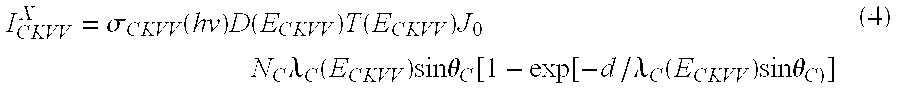
- equation (2) which includes equations (3) through (9), is appropriately considered as containing two parts, viz., (a) carbon Auger emission via x-ray excitation, and (b) carbon Auger emission via excitation by substrate photoelectrons.
- ⁇ CKVV ( h ⁇ ) is the cross-section for carbon Auger emission by x-ray excitation
- D( E CKVV ) is the efficiency of the electron detector
- T(E CKVV ) is the analyzer transmission function
- J 0 is the x-ray flux
- N c is the number of carbon atoms per cm 3
- ⁇ C (E CKVV ) is the inelastic mean free path of carbon Auger electrons in carbon
- ⁇ C is the angle of emission of carbon Auger electrons relative to the sample surface
- E CKVV is the kinetic energy of carbon Auger electrons
- hv is the x-ray energy
- I CKVV X ⁇ CKVV ⁇ ( h ⁇ ⁇ v ) ⁇ D ⁇ ( E CKVV ) ⁇ T ⁇ ( E CKVV ) ⁇ J 0 ⁇ N C ⁇ ⁇ C ⁇ ( E CKVV ) ⁇ ⁇ sin ⁇ ⁇ ⁇ C [ 1 - exp ⁇ [ - d / ⁇ C ⁇ ( E CKVV ) ⁇ ⁇ sin ⁇ ⁇ ⁇ C ) ] ( 4 )
- the flux of substrate photoelectrons crossing the substrate-carbon interface into the carbon overlayer will be used as a “source” term in an expression for carbon Auger emission via excitation by substrate photoelectrons.
- the substrate is composed of a single element of infinite thickness relative to the electron emission path lengths.
- n s i N s ⁇ J 0 ⁇ ⁇ s i ⁇ ( h ⁇ ⁇ v ) ⁇ ⁇ s ⁇ ( E s i ) ⁇ ⁇ sin ⁇ ⁇ ⁇ s ( 6 )
- Equation (7) represents the total substrate electron yield from the ith energy level that enters the carbon overlayer. To obtain the total number of substrate photoelectrons capable of causing a carbon Auger transition one sums over all states, i, with kinetic energy greater than the binding energy of C1s (285 eV).
- the Auger emission produced from a carbon layer of thickness d by the total incident electron flux n s is given by:
- ⁇ CKVV (E s i ) is the cross-section for carbon Auger emission upon bombardment by electrons from the ith substrate core level
- ⁇ C (E CKVV ) is the inelastic mean free path of carbon Auger electrons in carbon
- ⁇ C is the angle of emission of carbon Auger electrons with respect to the sample surface
- E CKVV is the kinetic energy of carbon Auger electrons.
- Equation (8) Integration of Equation (8) with respect to z yields the equation describing the total substrate photoelectron excited CKVV signal:
- Equation (9) can be viewed as the product of n s the substrate photo emission, the response of the carbonaceous overlayer to the substrate photoelectrons—N C ⁇ CKVV (E s i ) the instrumental response—T(E CKVV )D(E CKVV ), and a function representing the attenuation of the carbon Auger electrons in the overlayer.
- Energy loss of substrate photoelectrons in the overlayer has been ignored in this analysis. For overlayer thicknesses considered in this disclosure (less than 5 nm), this energy loss is small.
- the inventors calculated the ratio I CKVV e /I CKVV x using the Ebel model and the inventive Substrate Effect Model for a 2 nm thick carbonaceous layer on various substrates.
- the inventive Substrate Effect Model prediction was obtained by summing Equation (2) over all substrate transitions capable of causing ionization of a carbon atom in the overlayer. This includes emission of photoelectrons and Auger electrons from the substrate. The calculations were performed using a program written in BASIC, further discussed hereinbelow.
- FIG. 2 demonstrates that the general trend is a decrease in I C1s /I CKVV with increasing atomic number. Superimposed on this trend are variations in I C1s /I CKVV caused by the effect of substrate photoelectron energy on carbon excitation cross-section ⁇ C (E s i ) and IMFP within the carbon layer.
- FIG. 2 demonstrates that the inventive Substrate Effect Model is very similar to the Ebel Model for low atomic number substrates, but is appreciably different for higher atomic number substrates.
- Equation (2) demonstrates that the enhancement in the CKVV signal predicted by the inventive Substrate Effect Model depends linearly on n s i , the photoelectron emission from the substrate.
- n s i the photoelectron emission from the substrate.
- the large number of photoelectrons from high Z substrates increases the flux of carbon Auger electrons emitted from the carbonaceous layer.
- the C1s signal is not affected because the substrate photoelectrons exciting the C1s photoelectrons vary in energy.
- the I C1s /I CKVV ratio predicted by the inventive Substrate Effect Model is less than that predicted by the Ebel Model.
- FIG. 3 a through FIG. 3 f depict the carbon 1s to carbon KVV ratio predicted by the Ebel Model and the inventive Substrate Effect Model for a carbonaceous overlayer on six different substrates (aluminum, glass, titanium, copper, silver, and gold, respectively) as a function of overlayer thickness.
- the inventive Substrate Effect Model predicts a lower I C1s /I CKVV ratio than the Ebel Model for a given overlayer thickness; the exact difference between the two models depends on the substrate material and the overlayer thickness.
- FIG. 3 a through FIG. 3 f there is little difference between the Ebel Model and the inventive Substrate Effect Model for the lower Z substrates, glass and Aluminum.
- the program requires the following inputs: substrate density; molecular weight; plasmon energy; the beta, gamma, C and D terms in the modified Bethe formalism; and, the kinetic energies and photo ionization cross-sections of the substrate energy levels with kinetic energy greater than 285 eV.
- the data is inputted to the program in an ASCI file with the following format:
- laythick laythick+.1 ′layer thickness in nm
- FIG. 4 To test the predictions of the inventive Substrate Effect Model, the inventors measured the carbon 1s and carbon Auger peak intensities from carbonaceous overlayers of precisely controlled thickness on glass, aluminum, titanium, copper, silver and gold substrates. These substrates are predicted by the inventive Substrate Effect Model to have a wide variation in substrate-excited carbon Auger electron emission.
- the following six sets of samples were employed: (1) a set of alkane-thiol self-assembled monolayers on gold; (2) a set of alkyltrichlorosilane self-assembled monolayers on glass; (3) a Langmuir-Blodgett film of hexadecanoic acid on titanium; (4) a 10-carbon chain hydroxamic acid monolayer on silver; (5) a 14-carbon chain carboxylic acid monolayer on aluminum; and, (6) a 12-carbon chain amine on copper.
- XPS data were acquired using two different spectrometers: a Physical Electronics 5400 and a Physical Electronics 5600. Spectra were excited with Mg K ⁇ x-rays (1253.6 eV). Angle dependent XPS analysis was performed to verify overlayer thickness. ADXPS data were collected at five angles ranging from 15 to 80 degrees (relative to the surface plane). C1s and CKVV peaks were collected at each angle: Data collected at thirty degrees relative to the surface plane were used for the C1s/CKVV ratio data treatment.
- the substrate preparation and monolayer formation were performed in the ambient, except where noted otherwise.
- Gold substrates were prepared following the procedure given by Ulman. See Ulman, A., An Introduction to Ultrathin Organic Films , Academic Press, New York, New York, 1991, p 280.
- silanes The silane-based self-assembled monolayer were prepared following published procedures. See Stenger, D, J. Georger, C. Dulcey, J. Hickman, A. Rudolph, T. Nielson, S. McCort, J. Calvert. J. Am. Chem. Soc. 114, 8435-8442 (1992).
- Glass coverslips (Corning Glass Works, Corning, NY) were immersed in 50:50 HCI:MeOH for approximately 30 minutes, and then in boiling distilled water for approximately 30 minutes. The substrates were then baked at 150° C. for 2 hours to remove residual water.
- coverglasses were rinsed thoroughly with hexane. Outside the glovebag, the coverglasses were rinsed with isopropanol (Fisher), baked at 120° C. for 5 minutes, and rinsed again with isopropanol. The advancing contact angles of the silanized coverglasses were 95-100°.
- Each of these substrates was prepared from 99.99% metal foils, obtained from Alfa. The surfaces were mechanically polished to a final grit size of 0.3 micron to remove the bulk surface oxide. The copper and silver foils were chemically cleaned in dilute H 3 PO 4 for 30 seconds, and then cleaned ultrasonically in distilled water.
- the C 10 hydroxamic acid was belovedly supplied by the group of G. Whitesides, Harvard University, Cambridge Mass. Procedures for the preparation of hydroxamic acid layers on silver are described in a paper by this group. See Folkers, J., C. Gorman, P. Laibinis, S. Buchholz, G. Whitesides, R. Nuzzo. Langmuir 11(3), 813 (1995).
- Fatty acid (C 14 , R—COOH, Aldrich) monolayer on the aluminum surface were prepared following the descriptions provided in the papers by Laibinis et al. and Y. T. Tao. See Laibinis, P., J. Hickman, M. Wrighton, G. Whitesides. Science 245, 845 (1989). See also Tao Y. T. J. Am. Chem. Soc. 115, 4350 (1993).
- the inventors compared the measured I C1s /I CKVV ratio to those predicted by the Ebel and inventive Substrate Effect Models. These results are reported in FIG. 4 .
- FIG. 4 reports the overlayer thickness, measured I C1s /I CKVV ratio, the I C1s /I CKVV ratio calculated from the Ebel Model, the substrate effect correction (1+I c e /I C x ), and the I C1s /I CKVV ratio calculated from the inventive Substrate Effect Model for the various substrates assuming pure substrates (and overlayer thicknesses experimentally examined as disclosed herein).
- the error bars on the experimental data represent standard deviations of the mean, and were determined from the following data: aluminum and silver—two runs each on the Phi 5600 spectrometer; copper—three runs using the Phi 5600 spectrometer; titanium—one run each on the Phi 5400 and 5600 spectrometers; glass—five runs on the Phi 5400 spectrometer; gold—either three runs on the Phi 5400 spectrometer or one run each on the Phi 5400 and 5600 spectrometers.
- FIG. 4 The results reported in FIG. 4 demonstrate a general improvement between the measured I C1s /I CKVV ratios and the inventive Substrate Effect Model predictions, compared with the Ebel Model predictions. This is most evident for the gold substrate, as would be expected due to its large photoionization cross-section. This is further illustrated in FIG. 3 a through FIG. 3 f which, in addition to the model results discussed previously, also show the experimental data. The error bars represent standard deviations of the mean.
- the substrate effect correction appears too large. This is because the surfaces for aluminum, titanium, copper and silver are actually oxides under the ambient preparation conditions employed, and glass is a bulk oxide. In this case, the appropriate substrate effect correction must be based on the weighted emission cross-section of both metal and oxygen transitions.
- FIG. 4 summarizes the substrate effect results calculated in this way.
- inventive Substrate Effect Model is an accurate representation of the photo emission from the sample depicted in FIG. 1, for substrates of all compositions. Therefore, the inventive Substrate Effect Model can be employed to determine carbonaceous overlayer thicknesses, from I C1s /I CKVV data.
- step number 2 collect a survey scan on the sample of interest.
- the pass energy, analysis area and source to sample separation must be identical.
- inventive embodiments are directed to improving accuracy of XPS quantitative analysis.
- the invention increases accuracy with regard to the correction of the presence of an adventitious is carbonaceous overlayer in the quantitative analysis of XPS data.
- step number 7 will include, in addition to steps 1 through steps 6 above, the following step number 7:
Landscapes
- Physics & Mathematics (AREA)
- Chemical & Material Sciences (AREA)
- General Physics & Mathematics (AREA)
- Nanotechnology (AREA)
- Life Sciences & Earth Sciences (AREA)
- Health & Medical Sciences (AREA)
- Engineering & Computer Science (AREA)
- General Health & Medical Sciences (AREA)
- Spectroscopy & Molecular Physics (AREA)
- Crystallography & Structural Chemistry (AREA)
- Molecular Biology (AREA)
- Analytical Chemistry (AREA)
- Biochemistry (AREA)
- Immunology (AREA)
- Pathology (AREA)
- Electromagnetism (AREA)
- Analysing Materials By The Use Of Radiation (AREA)
Abstract
Description


Claims (18)
Priority Applications (1)
| Application Number | Priority Date | Filing Date | Title |
|---|---|---|---|
| US09/170,041 US6259092B1 (en) | 1998-10-13 | 1998-10-13 | Thickness determination of carbonaceous overlayers on substrates of differing material |
Applications Claiming Priority (1)
| Application Number | Priority Date | Filing Date | Title |
|---|---|---|---|
| US09/170,041 US6259092B1 (en) | 1998-10-13 | 1998-10-13 | Thickness determination of carbonaceous overlayers on substrates of differing material |
Publications (1)
| Publication Number | Publication Date |
|---|---|
| US6259092B1 true US6259092B1 (en) | 2001-07-10 |
Family
ID=22618305
Family Applications (1)
| Application Number | Title | Priority Date | Filing Date |
|---|---|---|---|
| US09/170,041 Expired - Fee Related US6259092B1 (en) | 1998-10-13 | 1998-10-13 | Thickness determination of carbonaceous overlayers on substrates of differing material |
Country Status (1)
| Country | Link |
|---|---|
| US (1) | US6259092B1 (en) |
Cited By (10)
| Publication number | Priority date | Publication date | Assignee | Title |
|---|---|---|---|---|
| US20020183193A1 (en) * | 2001-03-28 | 2002-12-05 | Asahi Glass Company, Limited | Process for preparing silicate porous product |
| WO2003067234A3 (en) * | 2002-02-04 | 2004-01-22 | Applied Materials Inc | Control of film growth using auger electron spectroscopy for measuring film thickness and chemical composition |
| US20040238735A1 (en) * | 2001-10-26 | 2004-12-02 | Larson Paul E. | System and method for depth profiling and characterization of thin films |
| US20060118718A1 (en) * | 2004-12-02 | 2006-06-08 | Sievers Michael R | Endpoint detection for the patterning of layered materials |
| US20060164656A1 (en) * | 2005-01-21 | 2006-07-27 | White Richard L | Method and system for measuring overcoat layer thickness on a thin film disk |
| US20060227321A1 (en) * | 2005-04-07 | 2006-10-12 | International Business Machines Corporation | Non-destructive in-situ elemental profiling |
| US7192649B1 (en) * | 2003-08-06 | 2007-03-20 | The United States Of America As Represented By The Secretary Of The Navy | Passivation layer on aluminum surface and method thereof |
| CN109931894A (en) * | 2019-03-26 | 2019-06-25 | 电子科技大学 | A method for analyzing the thickness of the oxide layer on the surface of NiFe or FeMn thin films |
| CN113310442A (en) * | 2021-04-27 | 2021-08-27 | 长江存储科技有限责任公司 | Thickness measuring method and device |
| US20210372786A1 (en) * | 2020-05-26 | 2021-12-02 | Samsung Electronics Co., Ltd. | Method of calculating thickness of graphene layer and method of measuring content of silicon carbide by using xps |
-
1998
- 1998-10-13 US US09/170,041 patent/US6259092B1/en not_active Expired - Fee Related
Non-Patent Citations (1)
| Title |
|---|
| Bruce Beard and Robert Brizzolara, Assessment of overlayer thickness determination model by controlled monolayers, J. Vac. Sci. Techno, A 14, Jan./Feb. 1996. * |
Cited By (18)
| Publication number | Priority date | Publication date | Assignee | Title |
|---|---|---|---|---|
| US20020183193A1 (en) * | 2001-03-28 | 2002-12-05 | Asahi Glass Company, Limited | Process for preparing silicate porous product |
| US20040238735A1 (en) * | 2001-10-26 | 2004-12-02 | Larson Paul E. | System and method for depth profiling and characterization of thin films |
| US7449682B2 (en) * | 2001-10-26 | 2008-11-11 | Revera Incorporated | System and method for depth profiling and characterization of thin films |
| WO2003067234A3 (en) * | 2002-02-04 | 2004-01-22 | Applied Materials Inc | Control of film growth using auger electron spectroscopy for measuring film thickness and chemical composition |
| US7192649B1 (en) * | 2003-08-06 | 2007-03-20 | The United States Of America As Represented By The Secretary Of The Navy | Passivation layer on aluminum surface and method thereof |
| US7285775B2 (en) | 2004-12-02 | 2007-10-23 | International Business Machines Corporation | Endpoint detection for the patterning of layered materials |
| US20060118718A1 (en) * | 2004-12-02 | 2006-06-08 | Sievers Michael R | Endpoint detection for the patterning of layered materials |
| US20060164656A1 (en) * | 2005-01-21 | 2006-07-27 | White Richard L | Method and system for measuring overcoat layer thickness on a thin film disk |
| US7362454B2 (en) * | 2005-01-21 | 2008-04-22 | Hitachi Global Storage Technologies Netherlands B.V. | Method and system for measuring overcoat layer thickness on a thin film disk |
| US7256399B2 (en) | 2005-04-07 | 2007-08-14 | International Business Machines Corporation | Non-destructive in-situ elemental profiling |
| US20060227321A1 (en) * | 2005-04-07 | 2006-10-12 | International Business Machines Corporation | Non-destructive in-situ elemental profiling |
| CN109931894A (en) * | 2019-03-26 | 2019-06-25 | 电子科技大学 | A method for analyzing the thickness of the oxide layer on the surface of NiFe or FeMn thin films |
| CN109931894B (en) * | 2019-03-26 | 2021-02-02 | 电子科技大学 | Method for analyzing thickness of surface oxide layer of NiFe or FeMn film |
| US20210372786A1 (en) * | 2020-05-26 | 2021-12-02 | Samsung Electronics Co., Ltd. | Method of calculating thickness of graphene layer and method of measuring content of silicon carbide by using xps |
| US11906291B2 (en) * | 2020-05-26 | 2024-02-20 | Samsung Electronics Co., Ltd. | Method of calculating thickness of graphene layer and method of measuring content of silicon carbide by using XPS |
| US20240151522A1 (en) * | 2020-05-26 | 2024-05-09 | Samsung Electronics Co., Ltd. | Method of calculating thickness of graphene layer and method of measuring content of silicon carbide by using xps |
| US12359911B2 (en) * | 2020-05-26 | 2025-07-15 | Samsung Electronics Co., Ltd. | Method of calculating thickness of graphene layer and method of measuring content of silicon carbide by using XPS |
| CN113310442A (en) * | 2021-04-27 | 2021-08-27 | 长江存储科技有限责任公司 | Thickness measuring method and device |
Similar Documents
| Publication | Publication Date | Title |
|---|---|---|
| Tougaard | Practical guide to the use of backgrounds in quantitative XPS | |
| Czanderna et al. | Beam effects, surface topography, and depth profiling in surface analysis | |
| Powell et al. | Surface sensitivity of X-ray photoelectron spectroscopy | |
| Giurlani et al. | Measuring the thickness of metal coatings: A review of the methods | |
| Tougaard | Improved XPS analysis by visual inspection of the survey spectrum | |
| Smith | Surface analysis by electron spectroscopy | |
| US6259092B1 (en) | Thickness determination of carbonaceous overlayers on substrates of differing material | |
| Castle | The use of X-ray photoelectron spectroscopy in corrosion science | |
| Powell | Growth of surface analysis and the development of databases and modeling software for Auger-electron spectroscopy and x-ray photoelectron spectroscopy | |
| Pollakowski et al. | Nondestructive and nonpreparative chemical nanometrology of internal material interfaces at tunable high information depths | |
| Giurlani et al. | Measuring the thickness of metal films: A selection guide to the most suitable technique | |
| Murdoch et al. | Quantitative depth‐dependent analysis using the inelastic scattering backgrounds from X‐ray photoelectron spectroscopy and hard X‐ray photoelectron spectroscopy | |
| Tougaard | HAXPES: Inelastic background for characterization of nanostructured materials | |
| Shard et al. | A simple approach to measuring thick organic films using the XPS inelastic background | |
| Powell et al. | Inelastic mean free paths, mean escape depths, information depths, and effective attenuation lengths for hard X-ray photoelectron spectroscopy | |
| Godet et al. | Bulk and surface plasmon excitations in amorphous carbon measured by core-level photoelectron spectroscopy | |
| Zhao et al. | Perspective—nano infrared microscopy: obtaining chemical information on the nanoscale in corrosion studies | |
| Pramanik et al. | Corrosion behavior of mild steel in the presence of urea, sodium chloride, potassium chloride, and glycine: a kinetic and potentiodynamic polarization study approach | |
| Anoikin et al. | Ultrathin protective overcoats on magnetic hard disks | |
| Baer et al. | Challenges in applying surface analysis methods to nanoparticles and nanostructured materials | |
| Norrman et al. | Lateral and vertical quantification of spin-coated polymer films on silicon by TOF-SIMS, XPS, and AFM | |
| Brizzolara et al. | Substrate photoelectron enhancement of carbonaceous overlayer Auger emission: effect of the substrate on carbon overlayer thickness determination in XPS | |
| Aiginger et al. | Principles and development of total reflection X-ray fluorescence analysis | |
| Bouckenooge et al. | On the use of AES data analysis to determine local enrichments of conversion coating elements at intermetallic particles on rolled Al | |
| Suzuki et al. | Level of consistency in quantification and IMFP determination by the Tougaard method applied to XPS of a Langmuir–Blodgett film taken at widely different emission angles |
Legal Events
| Date | Code | Title | Description |
|---|---|---|---|
| AS | Assignment |
Owner name: NAVY, UNITED STATES OF AMERICA, THE, AS REPRESENTE Free format text: ASSIGNMENT OF ASSIGNORS INTEREST;ASSIGNOR:BRIZZOLARA, ROBERT A.;REEL/FRAME:009691/0607 Effective date: 19981013 |
|
| AS | Assignment |
Owner name: NAVY, UNITED STATES OF AMERICA, THE, AS REPRESENT Free format text: ASSIGNMENT OF ASSIGNORS INTEREST;ASSIGNORS:AKZO NOBEL INC.;BEARD, BRUCE C.;REEL/FRAME:010091/0729 Effective date: 19990616 |
|
| FPAY | Fee payment |
Year of fee payment: 4 |
|
| FPAY | Fee payment |
Year of fee payment: 8 |
|
| REMI | Maintenance fee reminder mailed | ||
| LAPS | Lapse for failure to pay maintenance fees | ||
| STCH | Information on status: patent discontinuation |
Free format text: PATENT EXPIRED DUE TO NONPAYMENT OF MAINTENANCE FEES UNDER 37 CFR 1.362 |
|
| FP | Lapsed due to failure to pay maintenance fee |
Effective date: 20130710 |