US6239644B1 - Clock stretcher and level shifter with small component count and low power consumption - Google Patents
Clock stretcher and level shifter with small component count and low power consumption Download PDFInfo
- Publication number
- US6239644B1 US6239644B1 US09/445,191 US44519100A US6239644B1 US 6239644 B1 US6239644 B1 US 6239644B1 US 44519100 A US44519100 A US 44519100A US 6239644 B1 US6239644 B1 US 6239644B1
- Authority
- US
- United States
- Prior art keywords
- bus
- state
- bus device
- clock line
- level
- Prior art date
- Legal status (The legal status is an assumption and is not a legal conclusion. Google has not performed a legal analysis and makes no representation as to the accuracy of the status listed.)
- Expired - Lifetime
Links
Images


Classifications
-
- H—ELECTRICITY
- H03—ELECTRONIC CIRCUITRY
- H03K—PULSE TECHNIQUE
- H03K19/00—Logic circuits, i.e. having at least two inputs acting on one output; Inverting circuits
- H03K19/0175—Coupling arrangements; Interface arrangements
- H03K19/0185—Coupling arrangements; Interface arrangements using field effect transistors only
- H03K19/018507—Interface arrangements
-
- G—PHYSICS
- G06—COMPUTING OR CALCULATING; COUNTING
- G06F—ELECTRIC DIGITAL DATA PROCESSING
- G06F1/00—Details not covered by groups G06F3/00 - G06F13/00 and G06F21/00
- G06F1/04—Generating or distributing clock signals or signals derived directly therefrom
- G06F1/08—Clock generators with changeable or programmable clock frequency
-
- G—PHYSICS
- G06—COMPUTING OR CALCULATING; COUNTING
- G06F—ELECTRIC DIGITAL DATA PROCESSING
- G06F13/00—Interconnection of, or transfer of information or other signals between, memories, input/output devices or central processing units
- G06F13/38—Information transfer, e.g. on bus
- G06F13/42—Bus transfer protocol, e.g. handshake; Synchronisation
- G06F13/4204—Bus transfer protocol, e.g. handshake; Synchronisation on a parallel bus
- G06F13/4208—Bus transfer protocol, e.g. handshake; Synchronisation on a parallel bus being a system bus, e.g. VME bus, Futurebus, Multibus
- G06F13/4217—Bus transfer protocol, e.g. handshake; Synchronisation on a parallel bus being a system bus, e.g. VME bus, Futurebus, Multibus with synchronous protocol
-
- Y—GENERAL TAGGING OF NEW TECHNOLOGICAL DEVELOPMENTS; GENERAL TAGGING OF CROSS-SECTIONAL TECHNOLOGIES SPANNING OVER SEVERAL SECTIONS OF THE IPC; TECHNICAL SUBJECTS COVERED BY FORMER USPC CROSS-REFERENCE ART COLLECTIONS [XRACs] AND DIGESTS
- Y02—TECHNOLOGIES OR APPLICATIONS FOR MITIGATION OR ADAPTATION AGAINST CLIMATE CHANGE
- Y02D—CLIMATE CHANGE MITIGATION TECHNOLOGIES IN INFORMATION AND COMMUNICATION TECHNOLOGIES [ICT], I.E. INFORMATION AND COMMUNICATION TECHNOLOGIES AIMING AT THE REDUCTION OF THEIR OWN ENERGY USE
- Y02D10/00—Energy efficient computing, e.g. low power processors, power management or thermal management
Definitions
- the invention relates generally to an interface for a two-wire synchronous data communications bus, and relates more specifically to a interface to such a bus having a protocol in which any bus device can hold the data state by holding the clock line in a predetermined state, and in which the interface has small component count and low power consumption.
- the circuit also provides level shifting to minimize power consumption.
- microcomputer revolution began two decades ago, but for most of that time it was required only that the system being designed comply with rather unforgiving requirements of size (on the order of a desktop) and power consumption (several dozens or hundreds of watts).
- the early personal computers used large numbers of discrete components, but thereafter it became commonplace to use “chip sets” which reduce the computer system to half a dozen integrated circuits each with dozens or hundreds of pins, or preassembled “mother boards”, either of which leaves little or no room for optimization by the individual system designer. Thus the individual designer cannot do much in the way of reducing power consumption or changing physical size or form factor.
- the clock line is “high” in a quiescent state, and is pulled low if a device on the bus (the “bus master”) wishes to pass a bit of data on the line for reading by any or all of the devices on the bus.
- the bus master raises the clock line and again pulls the line low to indicate that a subsequent bit of data is readable by any or all of the devices on the bus. In this way a message composed of many data bits is communicated across the bus.
- any bus device having noted that the clock line has been pulled low, can itself pull the clock line low. Indeed in the general case it is assumed that any number of bus devices may have done so.
- the defined behavior of the bus master is to maintain the data level on the data line. In this way, a bus device can take as long as desired to read the data value (and to prepare for the reading of subsequent data values). In colloquial terms, it can be said that the clock line remains low until the slowest of the bus devices has managed to get up to speed and to process data on the data line.
- power consumption in a microprocessor or microcontroller is monotonically (and generally linearly) related to the clock speed thereof.
- the system designer who is attempting to maximize battery life (or to minimize power consumption) will consider a variety of measures including switching a microcontroller to a very slow clock speed, or indeed powering down the microcontroller, during times of low or zero workload. (This may be termed “putting the controller to sleep”.)
- the designer of a microcontroller for a computer keyboard may actually power down the microcontroller except when a key has been pressed. If the user makes a thousand keystrokes, the microcontroller is powered up and down a thousand times.
- a further concern is that there be minimal power leakage into any particular bus device while it is asleep.
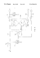
- FIG. 10 shows a typical prior art circuit that permits microcontroller 8051SL to go to sleep if desired and includes a clock stretching function.
- Four flip-flops (“start det”, “clk hold”, “busy”, and “stop”) are required along with several logic gates and comparators. There are many components to be assembled during manufacture and they take up space and consume power.
- a clock stretching circuit mediates between a synchronous bus and a microcontroller which is asleep most of the time to save electrical power.
- the bus is of a type in which a slow bus device can cause the sender of data to “hold” the data until the slow device is up to speed.
- the stretching circuit is of small component count and low power consumption and does not require any clocks.
- In one embodiment is comprised of a triple analog switch and a very small number of additional components.
- a dual four-position multiplexer is employed.
- four transistors are used with a handful of additional components.
- a level shifter including an MOSFET and a large-value resistor help to minimize power drain within the bus device.
- the components can be external to an off-the-shelf microcontroller or can be included in an IC that also contains an embedded microcontroller.
- FIG. 1 shows in functional block diagram form a generalized system including a synchronous communications bus, a microcontroller, and a clock stretching circuit, together with a power-saving level shifter;
- FIG. 2 shows in schematic form a clock stretching circuit employing a dual four-way multiplexer
- FIG. 3 shows a signal flow diagram for the circuit of FIG. 2
- FIG. 4 shows in schematic form a clock stretching circuit employing an MOSFET and three bipolar transistors
- FIG. 5 shows in schematic form a clock stretching circuit employing an MOSFET and three logic gates
- FIG. 6 shows in integrated circuit block diagram form a clock stretching circuit employing a triple analog switch
- FIG. 7 shows in schematic form the circuit of FIG. 6
- FIG. 8 shows in integrated circuit block diagram form the circuit of FIG. 2;
- FIG. 9 shows in schematic form a clock stretching circuit employing four bipolar transistors.
- FIG. 10 shows a prior-art clock stretching circuit.
- FIG. 1 shows in functional block diagram form a generalized system including a synchronous communications bus, a microcontroller (at 125 , 124 ), and a clock stretching circuit 110 , together with a power-saving level shifter (generally, 220 , 221 , 222 , 223 ).
- the purpose of the level shifters is to convert 0 to 5 signal swings on the bus into 0 to V+ swings on the microcontroller (bus device) pins 125 , 124 (for the V+ in the range of 2.7 to 3.3 volts) and to limit the leakage into the bus clock and bus data contacts 111 , 112 while the bus device is in total power-down (V+ is removed or at ground potential).
- the circuit for each of the bus clock and bus data lines I 1 , 112 consists of a single N-channel enhancement-mode MOSFET 220 , 221 (with V GS(th) ⁇ 1.5 volts), and a single resistor 222 , 223 , preferably a high-value pullup resistor ( ⁇ 100K ⁇ ). Operations of the level shifters for the clock and the data lines are the same, and the clock line 112 will be described.
- the drain is at the same (V+) or higher voltage.
- the intrinsic (parasitic) diode in the MOSFET structure is reverse-biased and does not conduct current.
- the intrinsic diode starts to conduct and initially develops a ⁇ 0.6 V drop from the drain to the source.
- the clock line 225 connected to the microcontroller (bus device) which is connected to the source of the MOSFET 221 follows the input voltage on the bus clock line 112 (but is higher by the ⁇ 0.6 V drop across the diode).
- the MOSFET 221 starts to develop enhancement voltage between the gate and source terminals.
- the MOSFET 221 When the input voltage reaches the level of [(V+) ⁇ (V GS(th) +V diode )], the MOSFET 221 begins to conduct current. As more current passes through the MOSFET 221 , the potential of the source is driven to the level of the bus clock line 112 on the drain. The process is regenerative and action is similar to a Schmitt trigger with ⁇ 0.6 V hysteresis. As the input bus clock line 112 level increases further, the MOSFET turns fully on, and brings the potential of the source 225 close to the level of the bus clock line 112 on the drain.
- the input voltage on the drain should be less than ⁇ 0.6 V in order to activate the MOSFET 221 (with V GS(th) ⁇ 1.5 V).
- the microcontroller's clock input line 225 follows the bus clock line 112 exactly until the level of [(V+)-(V GS(th) ], when the MOSFET 221 turns off, and the microcontroller's clock input line 225 starts to follow the bus clock line 112 with a positive offset of V diode .
- the pullup resistors 222 , 223 absorb small leakage currents from the MOSFETs 220 , 221 , the microcontroller and any additional circuitry connected to the translated/shifted clock and data lines 224 , 225 .
- FIG. 2 shows in schematic form a clock stretching circuit ( 110 , FIG. 1) employing a dual four-way multiplexer 162 , 163 preferably part number 74HC4052.
- the shifted clock line 225 connects with pin X 2 of multiplexer 162 , the common terminal of which is grounded. It also serves as one of the two binary inputs B, A which control the selections of the multiplexers 162 , 163 .
- B binary inputs
- A which control the selections of the multiplexers 162 , 163 .
- a binary count across binary values of B and A results in selection of selection lines 0 through 3.
- a synchronous bus having a clock line 225 with a first quiescent level (typically a positive voltage) and a second active level (ground) and a data line (omitted for clarity in FIG. 2 ), and with a bus device (also omitted for clarity in FIG. 2) having higher and lower power-consuming states; a clock stretcher (generally FIG. 2) comprising first and second four-position analog switches 162 , 163 , both of said switches controlled by a two-input binary control defining first and second inputs B and A.
- a clock stretcher generally FIG. 2 comprising first and second four-position analog switches 162 , 163 , both of said switches controlled by a two-input binary control defining first and second inputs B and A.
- the clock line 225 comprises the first one of said binary inputs, an output X 2 of the first analog switch 162 being open when said clock line 225 is at its first level and being at said second active level (grounded) when said first input A is at said second active level and said second input B is at a predetermined level; said output X 2 of said first analog switch 162 connected with said clock line 225 ; said output X 2 of said first analog switch 162 when at said second active level causing said bus device to transition from its lower-power-consuming-state to its higher-power-consuming state; said bus device further characterized in having a control output 161 ; said second four-position analog switch 163 characterized in that when said first input A is at said second active level and said second input B is at said predetermined level, said control output 161 is connected with said second input B.
- the output causing the bus device to transition from its lower-power-consuming-state to its higher-power-consuming state is connected to said bus device via line 225 , which is a different conductor from that of the control output 161 of the bus device.
- FIG. 3 shows a signal flow diagram for the circuit of FIG. 2 .
- the quiescent state 260 has the clock line high, and thus A is high.
- state 261 is entered.
- the microcontroller bus device
- the microcontroller is awakened from its low-power state and asserts (pulls low) the line 161 .
- This causes line B to go low for state 262 .
- the microcontroller de-asserts line 161 and the clock line is released.
- State 263 arrives, which is identical to state 260 .
- FIG. 4 shows in schematic form a clock stretching circuit ( 110 , FIG. 1) employing an MOSFET 215 and three bipolar transistors 210 , 212 , 213 .
- the FET is P-channel in this embodiment, transistors 212 and 213 are NPN, and transistor 210 is PNP.
- the first and second transistors 210 , 212 define a bistable gate having first and second states.
- the gate is electrically coupled with the clock line 225 .
- the clock line 225 When the clock line 225 is active low, this causes the gate to enter a state in which both transistors 210 , 211 are turned on. This pulls the clock line 225 low (active) which means that it stays low even after the external bus master device has stopped pulling the line low.
- the microcontroller (bus device) is responsive to the clock line entering its second active level (in this example, goes low) by entering said higher power-consuming state, and has a control output 216 .
- the gate is responsive to the control output by turning off the two transistors, permitting the clock line 225 to go high.
- FIG. 5 shows in schematic form a clock stretching circuit ( 110 , FIG. 1) employing an MOSFET 131 and three logic gates 132 , 133 , 134 .
- the gates 133 , 134 make up a flip-flop 138 .
- the flip-flop 138 responds to the clock line 225 going low by entering a state in which line 139 causes gate 132 to cause transistor 131 to turn on. Transistor 131 when turned on draws said clock line 225 low (active).
- the microcontroller (bus device) is fully up to speed and is capable of responding to the fact of the clock line having gone low. It then asserts control line 136 which resets the flip-flop 138 and permits line 139 to allow the transistor 131 to turn off.
- the signal interrupting the microprocessor to enter its higher-power-consuming state is line 137 , driven by the output of gate 132 .
- the signal interrupting the processor is connected with said bus device via a different conductor 137 from that of the control output 136 of the bus device.
- FIG. 6 shows in integrated circuit block diagram form a clock stretching circuit ( 110 , FIG. 1) employing a triple analog switch 123 . It is shown in more detail in FIG. 7 .
- Interrupt line 114 causes the microprocessor (bus device) to enter its high-power state.
- Switch 123 is preferably 74HC4053.
- FIG. 7 shows in schematic form the circuit of FIG. 6 .
- bus clock line 225 goes low (active)
- this turns off driver A and relaxing switch 120 , permitting line 114 to go high and turning on driver C.
- Line 114 is an interrupt to the microcontroller (bus device) and causes the microcontroller to enter its awake state.
- the microcontroller chooses to permit the data bus to proceed, it pulls line 114 low, turning off driver C and releasing the ground on line 225 Switch 121 together with external components provides a timing function.
- FIG. 8 shows in integrated circuit block diagram form the circuit of FIG. 2 .
- FIG. 9 shows in schematic form a clock stretching circuit employing four bipolar transistors 210 , 212 , 214 , 213 . Its theory of operation is largely in correspondence to the theory of operation of the system of FIG. 4 .
Landscapes
- Engineering & Computer Science (AREA)
- Theoretical Computer Science (AREA)
- Physics & Mathematics (AREA)
- General Engineering & Computer Science (AREA)
- Computer Hardware Design (AREA)
- General Physics & Mathematics (AREA)
- Computing Systems (AREA)
- Mathematical Physics (AREA)
- Logic Circuits (AREA)
- Manipulation Of Pulses (AREA)
Abstract
Description
Claims (12)
Priority Applications (1)
| Application Number | Priority Date | Filing Date | Title |
|---|---|---|---|
| US09/445,191 US6239644B1 (en) | 1997-07-09 | 1998-07-09 | Clock stretcher and level shifter with small component count and low power consumption |
Applications Claiming Priority (3)
| Application Number | Priority Date | Filing Date | Title |
|---|---|---|---|
| US5198097P | 1997-07-09 | 1997-07-09 | |
| US09/445,191 US6239644B1 (en) | 1997-07-09 | 1998-07-09 | Clock stretcher and level shifter with small component count and low power consumption |
| PCT/US1998/014325 WO1999003042A1 (en) | 1997-07-09 | 1998-07-09 | Clock stretcher and level shifter with small component count and low power consumption |
Publications (1)
| Publication Number | Publication Date |
|---|---|
| US6239644B1 true US6239644B1 (en) | 2001-05-29 |
Family
ID=21974619
Family Applications (1)
| Application Number | Title | Priority Date | Filing Date |
|---|---|---|---|
| US09/445,191 Expired - Lifetime US6239644B1 (en) | 1997-07-09 | 1998-07-09 | Clock stretcher and level shifter with small component count and low power consumption |
Country Status (3)
| Country | Link |
|---|---|
| US (1) | US6239644B1 (en) |
| CA (1) | CA2321051C (en) |
| WO (1) | WO1999003042A1 (en) |
Citations (5)
| Publication number | Priority date | Publication date | Assignee | Title |
|---|---|---|---|---|
| US4598216A (en) * | 1984-08-27 | 1986-07-01 | Ncr Corporation | Assist circuit for a data bus in a data processing system |
| US5371880A (en) * | 1992-05-13 | 1994-12-06 | Opti, Inc. | Bus synchronization apparatus and method |
| US5594874A (en) * | 1993-09-30 | 1997-01-14 | Cirrus Logic, Inc. | Automatic bus setting, sensing and switching interface unit |
| US5844438A (en) * | 1995-12-23 | 1998-12-01 | Samsung Electronics, Co., Ltd. | Circuit for generating an internal clock for data output buffers in a synchronous DRAM devices |
| US5877636A (en) * | 1996-10-18 | 1999-03-02 | Samsung Electronics Co., Ltd. | Synchronous multiplexer for clock signals |
-
1998
- 1998-07-09 WO PCT/US1998/014325 patent/WO1999003042A1/en not_active Ceased
- 1998-07-09 US US09/445,191 patent/US6239644B1/en not_active Expired - Lifetime
- 1998-07-09 CA CA002321051A patent/CA2321051C/en not_active Expired - Fee Related
Patent Citations (5)
| Publication number | Priority date | Publication date | Assignee | Title |
|---|---|---|---|---|
| US4598216A (en) * | 1984-08-27 | 1986-07-01 | Ncr Corporation | Assist circuit for a data bus in a data processing system |
| US5371880A (en) * | 1992-05-13 | 1994-12-06 | Opti, Inc. | Bus synchronization apparatus and method |
| US5594874A (en) * | 1993-09-30 | 1997-01-14 | Cirrus Logic, Inc. | Automatic bus setting, sensing and switching interface unit |
| US5844438A (en) * | 1995-12-23 | 1998-12-01 | Samsung Electronics, Co., Ltd. | Circuit for generating an internal clock for data output buffers in a synchronous DRAM devices |
| US5877636A (en) * | 1996-10-18 | 1999-03-02 | Samsung Electronics Co., Ltd. | Synchronous multiplexer for clock signals |
Also Published As
| Publication number | Publication date |
|---|---|
| WO1999003042A1 (en) | 1999-01-21 |
| CA2321051C (en) | 2003-11-25 |
| CA2321051A1 (en) | 1999-01-21 |
Similar Documents
| Publication | Publication Date | Title |
|---|---|---|
| US9189048B2 (en) | Circuit having a low power mode | |
| EP2239647B1 (en) | Motherboard with electronic device for reducing power consumption during sleep mode of computer motherboard | |
| US8195966B2 (en) | Electronic device for reducing power consumption during off of computer motherboard | |
| US6701442B1 (en) | Power management circuit for selectively applying power to network monitoring circuitry which monitors the receipt of network wake-up messages | |
| US20050253462A1 (en) | Integrated circuit with multiple power domains | |
| US8816741B2 (en) | State retention power gated cell | |
| KR20010038449A (en) | Power supply control circuit for computer system having a plurality of power management states | |
| US7032120B2 (en) | Method and apparatus for minimizing power requirements in a computer peripheral device while in suspend state and returning to full operation state without loss of data | |
| US7683697B2 (en) | Circuitry and method for buffering a power mode control signal | |
| US11372470B2 (en) | Control system for controlling intelligent system to reduce power consumption based on bluetooth device | |
| US8018247B2 (en) | Apparatus and method for reducing power consumption using selective power gating | |
| JP2000112587A5 (en) | ||
| CN112202432A (en) | Low-power-consumption key and external interrupt compatible wake-up circuit and control method thereof | |
| CN100499766C (en) | Quick starting TV set capable of implementing standby low power dissipation | |
| CN101625588B (en) | Supply circuit of PWM controller | |
| CN113672072B (en) | Method and apparatus for saving microcontroller power | |
| US6239644B1 (en) | Clock stretcher and level shifter with small component count and low power consumption | |
| US20050235169A1 (en) | Power reduction for unintentional activation of a wireless input device | |
| CN101872997A (en) | Continuous power supply switching control method and its device and power supply system | |
| CN210609113U (en) | One-key switching circuit | |
| CN112272022A (en) | Low-power-consumption external interrupt wake-up circuit and control method thereof | |
| CN211264190U (en) | A circuit with controllable power on and off | |
| CN221507441U (en) | Power supply control circuit, computer motherboard and computer equipment | |
| AU2013100559A4 (en) | Circuit having a low power mode | |
| CN221174779U (en) | RTC battery voltage detection circuit |
Legal Events
| Date | Code | Title | Description |
|---|---|---|---|
| AS | Assignment |
Owner name: USAR SYSTEMS, INC., NEW YORK Free format text: ASSIGNMENT OF ASSIGNORS INTEREST;ASSIGNORS:MARTEN, VICTOR;MILIOS, IOANNIS;WANG, WEI;REEL/FRAME:010528/0700 Effective date: 19991201 |
|
| AS | Assignment |
Owner name: USARSYS ACQUISITION CORP., NEW YORK Free format text: MERGER;ASSIGNOR:USAR SYSTEMS INCORPORATED;REEL/FRAME:010539/0826 Effective date: 19991206 |
|
| AS | Assignment |
Owner name: USAR SYSTEMS INCORPORATED, NEW YORK Free format text: RELEASE BY SECURED PARTY;ASSIGNOR:MTB BANK;REEL/FRAME:010648/0593 Effective date: 19991203 |
|
| STCF | Information on status: patent grant |
Free format text: PATENTED CASE |
|
| FPAY | Fee payment |
Year of fee payment: 4 |
|
| FPAY | Fee payment |
Year of fee payment: 8 |
|
| CC | Certificate of correction | ||
| AS | Assignment |
Owner name: JEFFERIES FINANCE LLC, NEW YORK Free format text: GRANT OF SECURITY INTEREST;ASSIGNORS:SEMTECH CORPORATION;SEMTECH NEW YORK CORPORATION;SIERRA MONOLITHICS, INC.;REEL/FRAME:027897/0141 Effective date: 20120320 |
|
| FPAY | Fee payment |
Year of fee payment: 12 |
|
| AS | Assignment |
Owner name: SEMTECH CORPORATION, CALIFORNIA Free format text: RELEASE BY SECURED PARTY;ASSIGNOR:JEFFERIES FINANCE LLC;REEL/FRAME:030341/0059 Effective date: 20130502 Owner name: SEMTECH NEW YORK CORPORATION, CALIFORNIA Free format text: RELEASE BY SECURED PARTY;ASSIGNOR:JEFFERIES FINANCE LLC;REEL/FRAME:030341/0059 Effective date: 20130502 Owner name: SIERRA MONOLITHICS, INC., CALIFORNIA Free format text: RELEASE BY SECURED PARTY;ASSIGNOR:JEFFERIES FINANCE LLC;REEL/FRAME:030341/0059 Effective date: 20130502 Owner name: HSBC BANK USA, NATIONAL ASSOCIATION, NEW YORK Free format text: SECURITY AGREEMENT;ASSIGNORS:SEMTECH CORPORATION;SEMTECH NEW YORK CORPORATION;SIERRA MONOLITHICS, INC.;REEL/FRAME:030341/0099 Effective date: 20130502 |
|
| AS | Assignment |
Owner name: HSBC BANK USA, NATIONAL ASSOCIATION, AS ADMINISTRATIVE AGENT, CALIFORNIA Free format text: SECURITY INTEREST;ASSIGNORS:SEMTECH CORPORATION;SEMTECH NEW YORK CORPORATION;SIERRA MONOLITHICS, INC.;AND OTHERS;SIGNING DATES FROM 20151115 TO 20161115;REEL/FRAME:040646/0799 Owner name: HSBC BANK USA, NATIONAL ASSOCIATION, AS ADMINISTRA Free format text: SECURITY INTEREST;ASSIGNORS:SEMTECH CORPORATION;SEMTECH NEW YORK CORPORATION;SIERRA MONOLITHICS, INC.;AND OTHERS;SIGNING DATES FROM 20151115 TO 20161115;REEL/FRAME:040646/0799 |
|
| AS | Assignment |
Owner name: JPMORGAN CHASE BANK, N.A., AS SUCCESSOR AGENT, ILLINOIS Free format text: ASSIGNMENT OF PATENT SECURITY INTEREST PREVIOUSLY RECORDED AT REEL/FRAME (040646/0799);ASSIGNOR:HSBC BANK USA, NATIONAL ASSOCIATION, AS RESIGNING AGENT;REEL/FRAME:062781/0544 Effective date: 20230210 |