US6239549B1 - Electron multiplier electron source and ionization source using it - Google Patents
Electron multiplier electron source and ionization source using it Download PDFInfo
- Publication number
- US6239549B1 US6239549B1 US09/004,911 US491198A US6239549B1 US 6239549 B1 US6239549 B1 US 6239549B1 US 491198 A US491198 A US 491198A US 6239549 B1 US6239549 B1 US 6239549B1
- Authority
- US
- United States
- Prior art keywords
- electron
- source
- electron source
- electrons
- microchannel plate
- Prior art date
- Legal status (The legal status is an assumption and is not a legal conclusion. Google has not performed a legal analysis and makes no representation as to the accuracy of the status listed.)
- Expired - Lifetime
Links
Images


Classifications
-
- H—ELECTRICITY
- H01—ELECTRIC ELEMENTS
- H01J—ELECTRIC DISCHARGE TUBES OR DISCHARGE LAMPS
- H01J49/00—Particle spectrometers or separator tubes
- H01J49/02—Details
- H01J49/08—Electron sources, e.g. for generating photo-electrons, secondary electrons or Auger electrons
-
- H—ELECTRICITY
- H01—ELECTRIC ELEMENTS
- H01J—ELECTRIC DISCHARGE TUBES OR DISCHARGE LAMPS
- H01J1/00—Details of electrodes, of magnetic control means, of screens, or of the mounting or spacing thereof, common to two or more basic types of discharge tubes or lamps
- H01J1/02—Main electrodes
- H01J1/32—Secondary-electron-emitting electrodes
-
- H—ELECTRICITY
- H01—ELECTRIC ELEMENTS
- H01J—ELECTRIC DISCHARGE TUBES OR DISCHARGE LAMPS
- H01J43/00—Secondary-emission tubes; Electron-multiplier tubes
- H01J43/04—Electron multipliers
-
- H—ELECTRICITY
- H01—ELECTRIC ELEMENTS
- H01J—ELECTRIC DISCHARGE TUBES OR DISCHARGE LAMPS
- H01J43/00—Secondary-emission tubes; Electron-multiplier tubes
- H01J43/04—Electron multipliers
- H01J43/06—Electrode arrangements
- H01J43/18—Electrode arrangements using essentially more than one dynode
- H01J43/24—Dynodes having potential gradient along their surfaces
- H01J43/246—Microchannel plates [MCP]
Definitions
- the present invention is directed to an ionization source for mass spectrometry or the like and to an electron source for such an ionization source.
- Analytical instrumentation is playing an expanded role in everyday life. Expanding applications include quality control, drug discovery, and medical diagnostics.
- Mass spectrometers are one of the most useful analytical instruments in use today. These devices provide compositional and structural information of unknown materials. The use of these instruments was originally limited to highly educated, specialized chemists known as mass spectroscopists. However, with the advent of low-cost computers with large memory capacity, a new generation of computer-controlled instruments, intended to be used by non-chemists, is now available. The use of on-board library spectra matching and identification has now enabled a whole new generation of non-technical professionals to benefit from the capabilities of these instruments. User-friendly instruments continue to expand the use of mass spectrometry into non-traditional market areas; indeed, a well-known restaurant chain now uses a mass spectrometer to check the quality of seafood before it is served.
- Mass spectrometer instruments include three basic parts: the ionization source, the mass filter, and the detector.
- the ionization source converts neutral molecules to be identified into ions.
- the mass filter separates the unknown ions from other ions in accordance with mass.
- the detector detects the ions by their mass and provides an amplified output signal, typically proportional to the abundance of the material present.
- the function of the ionization source is to apply a net charge to the neutral molecule which is to be identified. Ionization of a molecule is accomplished by adding electrons to the molecule or more often by subtracting electrons from the molecule. There are four common ionization techniques: electron impact, chemical ionization, field ionization, and photo ionization.
- FIG. 1 illustrates the typical filament-based ionization source employed in a current mass spectrometer.
- the narrow beam produced by the filament provided a relatively small area in which ions can be produced.
- the material to be ionized is introduced via gaseous sample inlet 102 to ionization space 104 .
- Cathodic filament electron emitter 106 supplied with filament heater potential 108 and electron accelerating potential 110 , emits a beam of electrons along electron trajectory 112 to electron discharge anode 114 .
- the beam of electrons ionizes the material to produce ion beam 116 which exits ionization space 104 through ion exit port 118 .
- Ion beam 116 passes through extracting lens 120 , focusing lens 122 and accelerating lens 124 to the analyzer.
- filament-based ionization sources have many performance disadvantages. They have a short life, typically 90 days. Heat generated by the filament can affect the chemistry of the molecule being identified. Filaments are unstable and require a warm-up period. Typical sources provide a narrow beam for collisions with molecules to be ionized.
- MCP microchannel plate
- An object of the invention is to provide an ionization source which overcomes the above-noted disadvantages.
- a further object of the invention is to provide a cold ionization source.
- a further object of the invention is to provide an ionization source having a large emission area.
- a further object of the invention is to provide an ionization source having a high-density, uniform emission pattern.
- a further object of the invention is to provide an ionization source which is durable and which will not burn out.
- a further object of the invention is to provide a low-maintenance ionization source which uses cold ionization and therefore does not require frequent cleaning.
- a further object of the invention is to provide an ionization source which does not require a warm-up/stabilization time.
- a further object of the invention is to provide an ionization source with fine emission level control.
- a further object of the invention is to provide an electron source which makes such an ionization source possible by not requiring a primary source to initiate emission and by not being limited to operation in the unstable ion feedback mode.
- the present invention is directed to an electron source comprising: a generating portion for spontaneously generating electrons; and an electron multiplying portion, receiving the electrons spontaneously generated by the generating portion, for multiplying the electrons to produce an electron beam.
- the present invention is further directed to a method of making an electron source, the method comprising the following steps: (a) forming an electron multiplier, and (b) treating the electron multiplier so that at least a portion of the electron multiplier spontaneously generates electrons.
- the invention is further directed to an ionization source comprising: an electron source including electron generating and multiplying portions for spontaneously generating electrons and multiplying the electrons to produce an electron beam; an ionization space disposed to receive the electron beam from the electron source, the ionization space having (i) an inlet for receiving a material to be ionized so that the material to be ionized passes through the electron beam to produce ions and (ii) an exit port for allowing the ions to exit the ionization space; and anode means, disposed in the ionization space, for discharging electrons in the electron beam from the ionization space once the electrons in the electron beam have passed through the ionization space.
- Electron multipliers can be processed in such a way as to spontaneously produce a stream of electrons when a high voltage is applied.
- the use of an electron multiplier (such as a microchannel plate, discrete dynode, or single-channel electron multiplier) as the source of electrons would provide a much larger area of high current density in which to produce ions. In this fashion, significant increases in ionization efficiency can be realized.
- an electron multiplier based electron source does not require the warm-up period and provides a longer useful lifetime.
- noisy electron multipliers which can be used to produce a stream of electrons for electron impact ionization sources.
- Process variations suitable for producing spontaneous emission electron multipliers can be used in the invention, as will be described in greater detail below.
- the noisy electron multiplier is in contrast to the quiet electron multiplier of White et al.
- the electron source according to the present invention is self-starting and does not require an external source to initiate or control the emission.
- an electron source operates both in and out of the ion feedback mode, as is required for all analytical instrumentation operation, thus providing fine emission control.
- FIG. 1 shows a filament-based ionization source according to the prior art
- FIG. 2 shows a first embodiment of the ionization source according to the present invention
- FIG. 3 shows a second embodiment of the ionization source for ensuring monoergic electron energy according to the present invention
- FIG. 4 shows a flow chart of a process used to produce a microchannel plate electron source for the ionization source of FIG. 2 or FIG. 3;
- FIG. 5 shows a portion of another microchannel plate electron source for the ionization source of FIG. 2 or FIG. 3;
- FIG. 6 shows an ionization source having a single-channel electron multiplier tube
- FIG. 7 shows an ionization source having discrete dynodes
- FIG. 8 shows two microchannel plates in a chevron configuration
- FIG. 9 shows two microchannel plates in a Z stack configuration
- FIG. 10 shows emission current from a chevron in ion runaway, the chevron configuration having a 5 ⁇ m pore size
- FIG. 11 shows the emission current in amperes as a function of applied voltage in kV for a single MCP, a chevron configuration, and a Z stack configuration
- FIGS. 12 and 13 show the emission current in amperes as a function of the applied voltage in kV in greater detail for the chevron configuration and the Z stack configuration, respectively;
- FIG. 14 shows the ion source emission current as a function of backfill argon chamber pressure
- FIG. 15 shows the percentage of initial emission current over time for no feedback and argon at 5 ⁇ 10 ⁇ 5 torr
- FIG. 16 shows the emission current as a function of applied voltage for a Z stack configuration and a pore size of 5 ⁇ m after 144 hours of operation.
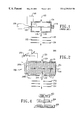
- FIG. 2 An ionization source in accordance with a first embodiment of the invention is shown in FIG. 2 .
- a specially processed microchannel plate is positioned at the beginning of an ionization cavity to serve as an electron source. The manner of special processing will be described in detail below.
- Microchannel plate (MCP) 206 used as an electron source has input and output faces 206 A, 206 B respectively.
- Microchannel plate electron source 206 is supplied with emission current supply voltage 208 between input face 206 A and output face 206 B.
- microchannel plate 206 emits a wide beam of electrons 215 along electron trajectory 212 to electron discharge anode 214 .
- the beam 215 of electrons ionizes the material 201 to produce ion beam 216 which exits ionization space 204 through ion exit port 218 .
- Ion beam 216 passes through extracting lens 220 , focusing lens 222 and accelerating lens 224 to the analyzer (not shown).
- emission current supply voltage 208 initiates the emission of electrons from output surface 206 B of microchannel plate 206 .
- Varying the voltage across microchannel plate 206 varies the emission current of beam 215 ; the emission current is roughly proportional to the applied voltage.
- no special start-up step is required.
- a series of grids 217 located adjacent to output surface 206 B of MCP 206 and connected to electron energy supply 210 is used to establish the impact energy of the electrons (typically 70 volts) and thus to establish the exit electron energy from MCP 206 .
- the large-area electron beam 215 traverses the ionization space 204 impact with the ambient molecules will result in the production of positive ions.
- Increasing the pressure within ionization space 204 , increasing the emission current, or doing both will increase ion production.
- the ionization space is constructed as a closed, conductive chamber bounded by the MCP and the anode.
- Voltage 208 is connected between input side 206 A of MCP 206 and ionization space 204 .
- Voltage 212 is connected between grids 217 and ionization space 204 .
- a second embodiment of an ionization source according to the present invention has a tunable electron source shown in FIG. 3 .
- Ionization source 300 in FIG. 3 is in many ways similar to ionization source 200 of FIG. 2 . That is, in ionization source 300 , the material 301 to be ionized is introduced via gaseous sample inlet 302 to ionization space 304 . MCP 306 , supplied with emission current supply voltage 308 and electron energy supply 310 voltage, emits a wide beam of electrons 315 along electron trajectory 312 to electron discharge anode 314 . The beam of electrons ionizes the material to produce ion beam 316 which exits ionization space 304 through ion exit port 318 . Ion beam 316 passes through extracting lens 320 , focusing lens 322 and accelerating lens 324 to the analyzer (not shown).
- ionization source 300 also includes high-energy electron discriminator 330 including voltage source 331 and electrode 332 and low-energy electron discriminator 334 including voltage source 335 , grid 336 and case 337 . Electrons leaving microchannel plate 306 travel past electrode 332 of high-energy electron discriminator 330 . Those electrons whose energy is below a first level, determined by the voltage applied to electrode 332 , follow trajectories 336 a toward ionization space 304 . Those electrons whose energy is above the first level follow trajectories 336 b away from ionization space 304 .
- Low-energy electrons following trajectories 336 a are incident on the grid 336 , which has a potential applied to it by the low-level energy discriminator 334 to form an energy barrier. Those electrons having energies above a second level determined by the grid. potential pass through grid 336 into ionization space 304 . Those electrons having energies below the second level do not pass through the grid 336 .
- Continuous electron multipliers such as MCP 206 or 306 can be made by various methods to emit electrons spontaneously when a high voltage is applied. Variations in the manufacturing processes which cause the emissive surface of the first strike conversion area (the area where, in conventional microchannel plates, the electron entering the channel would be incident and where the first electron multiplication would take place) to field emit free electrons will effectively transform the electron multiplier into an electron source.
- Single-channel electron multipliers and microchannel plates can be made to perform as spontaneous electron sources by subjecting the in-process device to an extended acid leaching step prior to the hydrogen reduction operation.
- step 404 of acid leaching is performed between step 402 of forming the microchannel plate and step 406 of hydrogen reduction, with steps 402 and 406 being performed through any suitable techniques such as those known in the art.
- Spontaneous electron emission may be obtained by these devices with any acid leaching process such as hydrochloric, acetic, nitric, or sulfuric acid solution of more than about 1% (by volume) for an exposure time exceeding about one minute, at a temperature above about 20 degrees centigrade.
- a second method for converting electron multipliers into spontaneous electron sources is achieved by coating the known first strike conversion surface 504 of a channel 502 in microchannel plate 500 with any alkali-containing compound 506 which will serve to lower the work function of the surface sufficiently to cause spontaneous electron emission.
- This approach will work for discrete dynode emitters as well as spontaneous electron emitters.
- FIGS. 4 and 5 are illustrative rather than limiting. Any technique for causing an electron multiplier to act as a spontaneous electron source can be used in the present invention.
- the ionization source or microchannel plate herein disclosed can be replaced by a single-channel electron multiplier, a discrete dynode multiplier, or other electron multiplier. Any electron multiplier having a source of spontaneously emitted electrons will suffice.
- Another possible variation is to use not a single MCP, but multiple MCP's in series. The MCP's can be arranged in a known chevron or Z configuration. Only the first MCP in the series is required to provide spontaneous electron emission.
- FIGS. 6-9. show schematic diagrams; those skilled in the art will appreciate that working embodiments may look different.
- electron sources are shown as discrete for the sake of clarity, although they may be formed integrally with other components in manners such as those described above.
- electrical connections are not shown, since those skilled in the art will readily understand where such electrical connections should be introduced.
- FIG. 6 shows an ionization source 600 including an electron source 602 and a single-channel electron multiplier tube 604 .
- An electron e leaving the source 600 enters the tube 602 and hits a wall, releasing more electrons. This process is repeated many times, so that a single electron e gives rise to multiple electrons e′ emerging from the far end of the tube 602 from the source 600 .
- FIG. 7 shows an ionization source 700 including an electron source 702 and discrete dynodes 704 , 706 , 708 , . . .
- An electron e leaving the source 700 hits a dynode 704 , which releases more electrons. This process is repeated for each of dynodes 706 , 708 , and so on, so that a single electron e gives rise to multiple electrons e′ emerging from the last dynode. While only three dynodes are shown, those skilled in the art will know how many to provide for proper operation in any application.
- FIGS. 8 and 9 show two configurations of two MCP's in series.
- FIG. 8 shows MCP's 802 and 804 in a chevron configuration
- FIG. 9 shows MCP's 902 and 904 in a Z stack configuration.
- MCP's 802 and 804 in a chevron configuration
- FIG. 9 shows MCP's 902 and 904 in a Z stack configuration.
- MCP's 902 and 904 in a Z stack configuration.
- they may be in a chevron, Z stack, or mixed configuration.
- FIG. 10 shows ion runaway for a chevron configuration with a 5 ⁇ m pore size.
- the emission current caused by ion runaway begins at a chevron voltage of 2 kV and exceeds 10 ⁇ A at less than 2.3 kV.
- FIG. 11 shows the emission current in amperes as a function of applied voltage in kV for a single MCP, a chevron configuration, and a Z stack configuration, each having a 5 ⁇ m pore size. In all three configurations, the emission current varies roughly linearly with the applied voltage.
- FIGS. 12 and 13 show the emission current in amperes as a function of the applied voltage in kV in greater detail for the chevron configuration and the Z stack configuration, respectively.
- FIG. 14 shows the ion source emission current as a function of backfill argon chamber pressure.
- FIG. 15 shows the percentage of initial emission current over time for no feedback and argon at 5 ⁇ 10 ⁇ 5 torr. The emission current peaks at one day of operation and asympototically approaches a value of less than 20% of initial emission current. After 144 hours of operation, the emission current as a function of applied voltage for a Z stack configuration and a pore size of 5 ⁇ m is shown in FIG. 16 .
- the electron source can be tuned in any suitable way.
- the material to be ionized can be introduced directly into the multiplier.
- the MCP electron source can be used in settings other than the ionization source; for example, a cathode-ray tube can be made thin (around 2 mm) by using an MCP as large as the desired display as the electron gun. Modifications described separately can be combined.
Abstract
Description
Claims (19)
Priority Applications (1)
| Application Number | Priority Date | Filing Date | Title |
|---|---|---|---|
| US09/004,911 US6239549B1 (en) | 1998-01-09 | 1998-01-09 | Electron multiplier electron source and ionization source using it |
Applications Claiming Priority (1)
| Application Number | Priority Date | Filing Date | Title |
|---|---|---|---|
| US09/004,911 US6239549B1 (en) | 1998-01-09 | 1998-01-09 | Electron multiplier electron source and ionization source using it |
Publications (1)
| Publication Number | Publication Date |
|---|---|
| US6239549B1 true US6239549B1 (en) | 2001-05-29 |
Family
ID=21713149
Family Applications (1)
| Application Number | Title | Priority Date | Filing Date |
|---|---|---|---|
| US09/004,911 Expired - Lifetime US6239549B1 (en) | 1998-01-09 | 1998-01-09 | Electron multiplier electron source and ionization source using it |
Country Status (1)
| Country | Link |
|---|---|
| US (1) | US6239549B1 (en) |
Cited By (13)
| Publication number | Priority date | Publication date | Assignee | Title |
|---|---|---|---|---|
| US20040026628A1 (en) * | 2002-04-27 | 2004-02-12 | Bruker Daltonik Gmbh | Device and method for moving an ion source |
| US20040041092A1 (en) * | 2002-08-29 | 2004-03-04 | Hamamatsu Photonics K.K. | Mass spectrometer and ion detector used therein |
| US20050218344A1 (en) * | 2004-04-05 | 2005-10-06 | Ronald Starcher | Controlled charge neutralization of ion-implanted articles |
| US20090015264A1 (en) * | 2007-07-11 | 2009-01-15 | Knott Richard A | Ionization gauge with a cold electron source |
| WO2009085165A2 (en) | 2007-12-19 | 2009-07-09 | Brooks Automation, Inc. | Ionization gauge having electron multiplier cold emmission source |
| US20100195801A1 (en) * | 2008-12-02 | 2010-08-05 | U.S.A. as represented by the Adminstrator of the National Aeronautics and Space Administration | Miniature, Low-Power X-Ray Tube Using A Microchannel Electron Generator Electron Source |
| US20110188634A1 (en) * | 2010-02-04 | 2011-08-04 | Suk-Yue Ka | X-ray generation device and cathode thereof |
| WO2013042830A1 (en) * | 2011-09-20 | 2013-03-28 | 한국기초과학지원연구원 | Device for obtaining the ion source of a mass spectrometer using an ultraviolet diode and a cem |
| WO2013042829A1 (en) * | 2011-09-20 | 2013-03-28 | 한국기초과학지원연구원 | Ultraviolet diode and atomic mass analysis ionization source collecting device using an ultraviolet diode and an mcp |
| US8410442B2 (en) | 2010-10-05 | 2013-04-02 | Nathaniel S. Hankel | Detector tube stack with integrated electron scrub system and method of manufacturing the same |
| KR101303242B1 (en) | 2011-11-25 | 2013-09-04 | 한국기초과학지원연구원 | Apparatus for Anion Generation and ECD using Cold Emission |
| US20140367568A1 (en) * | 2011-11-28 | 2014-12-18 | Korea Basic Science Institute | Anion generating and electron capture dissociation apparatus using cold electrons |
| EP2654072A3 (en) * | 2012-04-18 | 2016-01-27 | Bruker Daltonics, Inc. | Method and device for gas-phase ion fragmentation |
Citations (22)
| Publication number | Priority date | Publication date | Assignee | Title |
|---|---|---|---|---|
| US2150317A (en) | 1938-01-26 | 1939-03-14 | Rca Corp | Electron multiplier |
| US2586771A (en) | 1946-04-06 | 1952-02-26 | Int Standard Electric Corp | Process for making secondary emission electrodes |
| US2802127A (en) | 1954-02-03 | 1957-08-06 | Dobischek Dietrich | Dynode coating |
| US2810075A (en) | 1954-02-08 | 1957-10-15 | Cons Electrodynamics Corp | Mass spectrometry |
| US3171024A (en) | 1961-09-13 | 1965-02-23 | Bendix Corp | Narrow beam electron source for the ion source of a mass spectrometer |
| US3221164A (en) | 1959-09-25 | 1965-11-30 | Siemens Ag | Ion source for mass filter wherein the electron and ion beam axes are the same |
| US3586853A (en) | 1968-11-14 | 1971-06-22 | Scient Research Instr Corp | Axial beam time of flight mass spectrometer |
| US3663810A (en) | 1969-02-14 | 1972-05-16 | Stanford Research Inst | Electron-multiplier-ionizer mass spectrometer |
| US3854066A (en) | 1973-11-21 | 1974-12-10 | Us Army | Electron device incorporating a microchannel secondary emitter |
| US3904923A (en) * | 1974-01-14 | 1975-09-09 | Zenith Radio Corp | Cathodo-luminescent display panel |
| US4099079A (en) | 1975-10-30 | 1978-07-04 | U.S. Philips Corporation | Secondary-emissive layers |
| US4240007A (en) | 1979-06-29 | 1980-12-16 | International Business Machines Corporation | Microchannel ion gun |
| US4298817A (en) | 1979-08-13 | 1981-11-03 | Carette Jean Denis | Ion-electron source with channel multiplier having a feedback region |
| US4737623A (en) | 1985-05-28 | 1988-04-12 | Siemens Aktiengesellschaft | Canal structure of an electron multiplier |
| US4978885A (en) | 1989-03-02 | 1990-12-18 | Galileo Electro-Optics Corporation | Electron multipliers with reduced ion feedback |
| US5108961A (en) * | 1989-12-29 | 1992-04-28 | Circon Corporation | Etchable core glass compositions and method for manufacturing a high performance microchannel plate |
| US5132586A (en) | 1991-04-04 | 1992-07-21 | The United States Of America As Represented By The Secretary Of The Navy | Microchannel electron source |
| US5463218A (en) | 1993-05-19 | 1995-10-31 | Bruker-Franzen Analytik Gmbh | Detection of very large molecular ions in a time-of-flight mass spectrometer |
| US5656887A (en) * | 1995-08-10 | 1997-08-12 | Micron Display Technology, Inc. | High efficiency field emission display |
| US5656807A (en) * | 1995-09-22 | 1997-08-12 | Packard; Lyle E. | 360 degrees surround photon detector/electron multiplier with cylindrical photocathode defining an internal detection chamber |
| US5729244A (en) * | 1995-04-04 | 1998-03-17 | Lockwood; Harry F. | Field emission device with microchannel gain element |
| US5751109A (en) * | 1996-07-08 | 1998-05-12 | United States Of America As Represented By The Administrator, National Aeronautics And Space Administration | Segmented cold cathode display panel |
-
1998
- 1998-01-09 US US09/004,911 patent/US6239549B1/en not_active Expired - Lifetime
Patent Citations (22)
| Publication number | Priority date | Publication date | Assignee | Title |
|---|---|---|---|---|
| US2150317A (en) | 1938-01-26 | 1939-03-14 | Rca Corp | Electron multiplier |
| US2586771A (en) | 1946-04-06 | 1952-02-26 | Int Standard Electric Corp | Process for making secondary emission electrodes |
| US2802127A (en) | 1954-02-03 | 1957-08-06 | Dobischek Dietrich | Dynode coating |
| US2810075A (en) | 1954-02-08 | 1957-10-15 | Cons Electrodynamics Corp | Mass spectrometry |
| US3221164A (en) | 1959-09-25 | 1965-11-30 | Siemens Ag | Ion source for mass filter wherein the electron and ion beam axes are the same |
| US3171024A (en) | 1961-09-13 | 1965-02-23 | Bendix Corp | Narrow beam electron source for the ion source of a mass spectrometer |
| US3586853A (en) | 1968-11-14 | 1971-06-22 | Scient Research Instr Corp | Axial beam time of flight mass spectrometer |
| US3663810A (en) | 1969-02-14 | 1972-05-16 | Stanford Research Inst | Electron-multiplier-ionizer mass spectrometer |
| US3854066A (en) | 1973-11-21 | 1974-12-10 | Us Army | Electron device incorporating a microchannel secondary emitter |
| US3904923A (en) * | 1974-01-14 | 1975-09-09 | Zenith Radio Corp | Cathodo-luminescent display panel |
| US4099079A (en) | 1975-10-30 | 1978-07-04 | U.S. Philips Corporation | Secondary-emissive layers |
| US4240007A (en) | 1979-06-29 | 1980-12-16 | International Business Machines Corporation | Microchannel ion gun |
| US4298817A (en) | 1979-08-13 | 1981-11-03 | Carette Jean Denis | Ion-electron source with channel multiplier having a feedback region |
| US4737623A (en) | 1985-05-28 | 1988-04-12 | Siemens Aktiengesellschaft | Canal structure of an electron multiplier |
| US4978885A (en) | 1989-03-02 | 1990-12-18 | Galileo Electro-Optics Corporation | Electron multipliers with reduced ion feedback |
| US5108961A (en) * | 1989-12-29 | 1992-04-28 | Circon Corporation | Etchable core glass compositions and method for manufacturing a high performance microchannel plate |
| US5132586A (en) | 1991-04-04 | 1992-07-21 | The United States Of America As Represented By The Secretary Of The Navy | Microchannel electron source |
| US5463218A (en) | 1993-05-19 | 1995-10-31 | Bruker-Franzen Analytik Gmbh | Detection of very large molecular ions in a time-of-flight mass spectrometer |
| US5729244A (en) * | 1995-04-04 | 1998-03-17 | Lockwood; Harry F. | Field emission device with microchannel gain element |
| US5656887A (en) * | 1995-08-10 | 1997-08-12 | Micron Display Technology, Inc. | High efficiency field emission display |
| US5656807A (en) * | 1995-09-22 | 1997-08-12 | Packard; Lyle E. | 360 degrees surround photon detector/electron multiplier with cylindrical photocathode defining an internal detection chamber |
| US5751109A (en) * | 1996-07-08 | 1998-05-12 | United States Of America As Represented By The Administrator, National Aeronautics And Space Administration | Segmented cold cathode display panel |
Non-Patent Citations (4)
| Title |
|---|
| Exhibit Book for U.S. Patent Appln. Serial No. 317,977, filed Mar. 2, 1989 (Paul L. White et al., applicants), for "Electron Multipliers with Reduced Ion Feedback". |
| Timothy, J. G., "Preliminary Results with Microchannel Array Plates Employing Curved Microchannels to Inhibit Ion Feedback", Rev. Sci. Instrum. vol. 48, No. 3, Mar. 1977, pp. 292-299. |
| Timothy, J. Gethyn, "Curved-Channel Microchannel Array Plates", Rev. Sci. Instrum. vol. 52 No. 8, Aug. 1981, pp. 1131-1142. |
| Timothy, J. Gethyn, Mount, George H., and Bybee, Richard L., "Multi-Anode Microchannel Arrays", SPIE vol. 190 LASL Optics Conference (1979), pp. 360-368. |
Cited By (31)
| Publication number | Priority date | Publication date | Assignee | Title |
|---|---|---|---|---|
| US6828549B2 (en) | 2002-04-27 | 2004-12-07 | Bruker Daltonik Gmbh | Apparatus and method for moving an electron source |
| US20040026628A1 (en) * | 2002-04-27 | 2004-02-12 | Bruker Daltonik Gmbh | Device and method for moving an ion source |
| US20040041092A1 (en) * | 2002-08-29 | 2004-03-04 | Hamamatsu Photonics K.K. | Mass spectrometer and ion detector used therein |
| US6707034B1 (en) * | 2002-08-29 | 2004-03-16 | Hamamatsu Photonics K.K. | Mass spectrometer and ion detector used therein |
| US20050218344A1 (en) * | 2004-04-05 | 2005-10-06 | Ronald Starcher | Controlled charge neutralization of ion-implanted articles |
| EP1585166A2 (en) * | 2004-04-05 | 2005-10-12 | Burle Technologies, Inc. | Controlled charge neutralization of Ion-implanted articles |
| JP2005294269A (en) * | 2004-04-05 | 2005-10-20 | Burle Technologies Inc | Neutralization of controlled charge of ion implanted workpiece |
| US7038223B2 (en) | 2004-04-05 | 2006-05-02 | Burle Technologies, Inc. | Controlled charge neutralization of ion-implanted articles |
| US7768267B2 (en) | 2007-07-11 | 2010-08-03 | Brooks Automation, Inc. | Ionization gauge with a cold electron source |
| US20090015264A1 (en) * | 2007-07-11 | 2009-01-15 | Knott Richard A | Ionization gauge with a cold electron source |
| US20110234233A1 (en) * | 2007-12-19 | 2011-09-29 | Brucker Gerardo A | Ionization Gauge Having Electron Multiplier Cold Emission Source |
| JP2011508211A (en) * | 2007-12-19 | 2011-03-10 | ブルックス オートメーション インコーポレイテッド | An ionization gauge with a cold electron multiplier emission source |
| WO2009085165A2 (en) | 2007-12-19 | 2009-07-09 | Brooks Automation, Inc. | Ionization gauge having electron multiplier cold emmission source |
| EP2232224A4 (en) * | 2007-12-19 | 2015-07-01 | Mks Instr Inc | Ionization gauge having electron multiplier cold emmission source |
| US8686733B2 (en) * | 2007-12-19 | 2014-04-01 | Brooks Automation, Inc. | Ionization gauge having electron multiplier cold emission source |
| US8081734B2 (en) | 2008-12-02 | 2011-12-20 | The United States Of America As Represented By The Administrator Of The National Aeronautics And Space Administration | Miniature, low-power X-ray tube using a microchannel electron generator electron source |
| US20100195801A1 (en) * | 2008-12-02 | 2010-08-05 | U.S.A. as represented by the Adminstrator of the National Aeronautics and Space Administration | Miniature, Low-Power X-Ray Tube Using A Microchannel Electron Generator Electron Source |
| US8559599B2 (en) * | 2010-02-04 | 2013-10-15 | Energy Resources International Co., Ltd. | X-ray generation device and cathode thereof |
| US20110188634A1 (en) * | 2010-02-04 | 2011-08-04 | Suk-Yue Ka | X-ray generation device and cathode thereof |
| US8410442B2 (en) | 2010-10-05 | 2013-04-02 | Nathaniel S. Hankel | Detector tube stack with integrated electron scrub system and method of manufacturing the same |
| KR101319925B1 (en) * | 2011-09-20 | 2013-10-21 | 한국기초과학지원연구원 | Apparatus for Acquiring Ion source of Mass spectrometry using UV LED and CEM |
| KR101319926B1 (en) | 2011-09-20 | 2013-10-29 | 한국기초과학지원연구원 | Apparatus for Acquiring Ion source of Mass spectrometry using UV LED and MCP |
| WO2013042829A1 (en) * | 2011-09-20 | 2013-03-28 | 한국기초과학지원연구원 | Ultraviolet diode and atomic mass analysis ionization source collecting device using an ultraviolet diode and an mcp |
| US20140339423A1 (en) * | 2011-09-20 | 2014-11-20 | Korea Basic Science Institute | Ultraviolet diode and atomic mass analysis ionization source collecting device using ultraviolet diode and an mcp |
| US8927943B2 (en) * | 2011-09-20 | 2015-01-06 | Korea Basic Science Institute | Device for obtaining the ion source of a mass spectrometer using an ultraviolet diode and a CEM |
| US8981289B2 (en) * | 2011-09-20 | 2015-03-17 | Korea Basic Science Institute | Ultraviolet diode and atomic mass analysis ionization source collecting device using ultraviolet diode and an MCP |
| WO2013042830A1 (en) * | 2011-09-20 | 2013-03-28 | 한국기초과학지원연구원 | Device for obtaining the ion source of a mass spectrometer using an ultraviolet diode and a cem |
| KR101303242B1 (en) | 2011-11-25 | 2013-09-04 | 한국기초과학지원연구원 | Apparatus for Anion Generation and ECD using Cold Emission |
| US20140367568A1 (en) * | 2011-11-28 | 2014-12-18 | Korea Basic Science Institute | Anion generating and electron capture dissociation apparatus using cold electrons |
| US9230791B2 (en) * | 2011-11-28 | 2016-01-05 | Korea Basic Science Institute | Anion generating and electron capture dissociation apparatus using cold electrons |
| EP2654072A3 (en) * | 2012-04-18 | 2016-01-27 | Bruker Daltonics, Inc. | Method and device for gas-phase ion fragmentation |
Similar Documents
| Publication | Publication Date | Title |
|---|---|---|
| US5572022A (en) | Method and apparatus of increasing dynamic range and sensitivity of a mass spectrometer | |
| EP1875486B1 (en) | Method for controlling space charge-driven ion instabilities in electron impact ion sources | |
| US6958472B2 (en) | Mass spectrometry methods using electron capture by ions | |
| US7329864B2 (en) | Mass spectrometry with multiple ionization sources and multiple mass analyzers | |
| US6239549B1 (en) | Electron multiplier electron source and ionization source using it | |
| US3553452A (en) | Time-of-flight mass spectrometer operative at elevated ion source pressures | |
| JP4463978B2 (en) | Method and apparatus for selective collision-induced dissociation of ions in a quadrupole ion guide | |
| EP2819144B1 (en) | Axial magnetic field ion source and related ionization methods | |
| EP2363877A1 (en) | Method for chemical analysis | |
| Stoffels et al. | Electron attachment mass spectrometry as a diagnostics for electronegative gases and plasmas | |
| JP6739931B2 (en) | Ion source for soft electron ionization and related systems and methods | |
| WO1983002572A1 (en) | Sputter initiated resonance ionization spectrometry | |
| US8217343B2 (en) | Device and method using microplasma array for ionizing samples for mass spectrometry | |
| US3849656A (en) | Plural sample ion source | |
| US4988869A (en) | Method and apparatus for electron-induced dissociation of molecular species | |
| US8081734B2 (en) | Miniature, low-power X-ray tube using a microchannel electron generator electron source | |
| Larsson et al. | Wavelengths and energy levels of Xe vii and Xe viii obtained by collision-based spectroscopy | |
| US7038199B2 (en) | Apparatus and method for elemental mass spectrometry | |
| Murray et al. | IUPAC standard definitions of terms relating to mass spectrometry | |
| Steiner et al. | Glow discharge optical spectroscopy and mass spectrometry | |
| Geno | Ion detection in mass spectrometry | |
| Baudin et al. | A spontaneous desorption source for polyatomic ion production | |
| Fountain | Activation and fragmentation of peptides in time-of-flight mass spectrometry using optical and non-optical ionization sources | |
| Himura et al. | Formation of Pseudo Ions in Nested Penning Traps in Plasma Translation Experiment | |
| Bogaerts | Glow Discharge Optical Spectroscopy and Mass Spectrometry |
Legal Events
| Date | Code | Title | Description |
|---|---|---|---|
| AS | Assignment |
Owner name: GALILEO CORPORATION, MASSACHUSETTS Free format text: ASSIGNMENT OF ASSIGNORS INTEREST;ASSIGNOR:LAPRADE, BRUCE;REEL/FRAME:009210/0980 Effective date: 19980512 |
|
| STCF | Information on status: patent grant |
Free format text: PATENTED CASE |
|
| FPAY | Fee payment |
Year of fee payment: 4 |
|
| FPAY | Fee payment |
Year of fee payment: 8 |
|
| AS | Assignment |
Owner name: ING BANK N.V., LONDON BRANCH, UNITED KINGDOM Free format text: SECURITY AGREEMENT;ASSIGNOR:BURLE TECHNOLOGIES, INC.;REEL/FRAME:027891/0405 Effective date: 20120319 |
|
| FPAY | Fee payment |
Year of fee payment: 12 |
|
| AS | Assignment |
Owner name: BURLE TECHNOLOGIES, INC., PENNSYLVANIA Free format text: RELEASE BY SECURED PARTY;ASSIGNOR:ING BANK N.V., LONDON BRANCH;REEL/FRAME:031235/0941 Effective date: 20130918 |
|
| AS | Assignment |
Owner name: CREDIT SUISSE AG AS COLLATERAL AGENT, NEW YORK Free format text: SECURITY AGREEMENT;ASSIGNOR:BURLE TECHNOLOGIES, LLC;REEL/FRAME:031247/0396 Effective date: 20130918 |
|
| AS | Assignment |
Owner name: CREDIT SUISSE, AG, CAYMAN ISLANDS BRANCH, AS COLLA Free format text: SECURITY INTEREST;ASSIGNORS:BURLE TECHNOLOGIES;PHOTONIS SCIENTIFIC, INC.;PHOTONIS NETHERLANDS B.V.;AND OTHERS;REEL/FRAME:048357/0067 Effective date: 20180701 |
|
| AS | Assignment |
Owner name: PHOTONIS NETHERLANDS, B.V., NETHERLANDS Free format text: RELEASE OF INTELLECTUAL PROPERTY SECURITY INTERESTS AT R/F 048357/0067;ASSIGNOR:CREDIT SUISSE AG, CAYMAN ISLANDS BRANCH, AS COLLATERAL AGENT;REEL/FRAME:058887/0384 Effective date: 20220127 Owner name: PHOTONIS FRANCE SAS, FRANCE Free format text: RELEASE OF INTELLECTUAL PROPERTY SECURITY INTERESTS AT R/F 048357/0067;ASSIGNOR:CREDIT SUISSE AG, CAYMAN ISLANDS BRANCH, AS COLLATERAL AGENT;REEL/FRAME:058887/0384 Effective date: 20220127 Owner name: PHOTONIS SCIENTIFIC, INC., MASSACHUSETTS Free format text: RELEASE OF INTELLECTUAL PROPERTY SECURITY INTERESTS AT R/F 048357/0067;ASSIGNOR:CREDIT SUISSE AG, CAYMAN ISLANDS BRANCH, AS COLLATERAL AGENT;REEL/FRAME:058887/0384 Effective date: 20220127 Owner name: PHOTONIS DEFENSE, INC., PENNSYLVANIA Free format text: RELEASE OF INTELLECTUAL PROPERTY SECURITY INTERESTS AT R/F 048357/0067;ASSIGNOR:CREDIT SUISSE AG, CAYMAN ISLANDS BRANCH, AS COLLATERAL AGENT;REEL/FRAME:058887/0384 Effective date: 20220127 Owner name: BURLE TECHNOLOGIES, LLC, DELAWARE Free format text: RELEASE OF INTELLECTUAL PROPERTY SECURITY INTERESTS AT R/F 048357/0067;ASSIGNOR:CREDIT SUISSE AG, CAYMAN ISLANDS BRANCH, AS COLLATERAL AGENT;REEL/FRAME:058887/0384 Effective date: 20220127 |
|
| AS | Assignment |
Owner name: AETHER FINANCIAL SERVICES SAS, AS SECURITY AGENT, FRANCE Free format text: SECURITY INTEREST;ASSIGNOR:PHOTONIS SCIENTIFIC, INC.;REEL/FRAME:058808/0959 Effective date: 20220128 |