US6207561B1 - Selective oxidation methods for metal oxide deposition on metals in capacitor fabrication - Google Patents
Selective oxidation methods for metal oxide deposition on metals in capacitor fabrication Download PDFInfo
- Publication number
- US6207561B1 US6207561B1 US09/363,801 US36380199A US6207561B1 US 6207561 B1 US6207561 B1 US 6207561B1 US 36380199 A US36380199 A US 36380199A US 6207561 B1 US6207561 B1 US 6207561B1
- Authority
- US
- United States
- Prior art keywords
- metal
- oxidation
- over
- forming
- oxide layer
- Prior art date
- Legal status (The legal status is an assumption and is not a legal conclusion. Google has not performed a legal analysis and makes no representation as to the accuracy of the status listed.)
- Expired - Lifetime
Links
Images
Classifications
-
- H—ELECTRICITY
- H01—ELECTRIC ELEMENTS
- H01L—SEMICONDUCTOR DEVICES NOT COVERED BY CLASS H10
- H01L21/00—Processes or apparatus adapted for the manufacture or treatment of semiconductor or solid state devices or of parts thereof
- H01L21/02—Manufacture or treatment of semiconductor devices or of parts thereof
- H01L21/02104—Forming layers
- H01L21/02107—Forming insulating materials on a substrate
- H01L21/02225—Forming insulating materials on a substrate characterised by the process for the formation of the insulating layer
- H01L21/02227—Forming insulating materials on a substrate characterised by the process for the formation of the insulating layer formation by a process other than a deposition process
- H01L21/0223—Forming insulating materials on a substrate characterised by the process for the formation of the insulating layer formation by a process other than a deposition process formation by oxidation, e.g. oxidation of the substrate
- H01L21/02244—Forming insulating materials on a substrate characterised by the process for the formation of the insulating layer formation by a process other than a deposition process formation by oxidation, e.g. oxidation of the substrate of a metallic layer
-
- H—ELECTRICITY
- H01—ELECTRIC ELEMENTS
- H01L—SEMICONDUCTOR DEVICES NOT COVERED BY CLASS H10
- H01L21/00—Processes or apparatus adapted for the manufacture or treatment of semiconductor or solid state devices or of parts thereof
- H01L21/02—Manufacture or treatment of semiconductor devices or of parts thereof
- H01L21/04—Manufacture or treatment of semiconductor devices or of parts thereof the devices having at least one potential-jump barrier or surface barrier, e.g. PN junction, depletion layer or carrier concentration layer
- H01L21/18—Manufacture or treatment of semiconductor devices or of parts thereof the devices having at least one potential-jump barrier or surface barrier, e.g. PN junction, depletion layer or carrier concentration layer the devices having semiconductor bodies comprising elements of Group IV of the Periodic System or AIIIBV compounds with or without impurities, e.g. doping materials
- H01L21/30—Treatment of semiconductor bodies using processes or apparatus not provided for in groups H01L21/20 - H01L21/26
- H01L21/31—Treatment of semiconductor bodies using processes or apparatus not provided for in groups H01L21/20 - H01L21/26 to form insulating layers thereon, e.g. for masking or by using photolithographic techniques; After treatment of these layers; Selection of materials for these layers
- H01L21/314—Inorganic layers
- H01L21/316—Inorganic layers composed of oxides or glassy oxides or oxide based glass
- H01L21/31604—Deposition from a gas or vapour
-
- H—ELECTRICITY
- H01—ELECTRIC ELEMENTS
- H01L—SEMICONDUCTOR DEVICES NOT COVERED BY CLASS H10
- H01L21/00—Processes or apparatus adapted for the manufacture or treatment of semiconductor or solid state devices or of parts thereof
- H01L21/02—Manufacture or treatment of semiconductor devices or of parts thereof
- H01L21/04—Manufacture or treatment of semiconductor devices or of parts thereof the devices having at least one potential-jump barrier or surface barrier, e.g. PN junction, depletion layer or carrier concentration layer
- H01L21/18—Manufacture or treatment of semiconductor devices or of parts thereof the devices having at least one potential-jump barrier or surface barrier, e.g. PN junction, depletion layer or carrier concentration layer the devices having semiconductor bodies comprising elements of Group IV of the Periodic System or AIIIBV compounds with or without impurities, e.g. doping materials
- H01L21/30—Treatment of semiconductor bodies using processes or apparatus not provided for in groups H01L21/20 - H01L21/26
- H01L21/31—Treatment of semiconductor bodies using processes or apparatus not provided for in groups H01L21/20 - H01L21/26 to form insulating layers thereon, e.g. for masking or by using photolithographic techniques; After treatment of these layers; Selection of materials for these layers
- H01L21/314—Inorganic layers
- H01L21/316—Inorganic layers composed of oxides or glassy oxides or oxide based glass
- H01L21/3165—Inorganic layers composed of oxides or glassy oxides or oxide based glass formed by oxidation
- H01L21/31683—Inorganic layers composed of oxides or glassy oxides or oxide based glass formed by oxidation of metallic layers, e.g. Al deposited on the body, e.g. formation of multi-layer insulating structures
-
- H—ELECTRICITY
- H01—ELECTRIC ELEMENTS
- H01L—SEMICONDUCTOR DEVICES NOT COVERED BY CLASS H10
- H01L21/00—Processes or apparatus adapted for the manufacture or treatment of semiconductor or solid state devices or of parts thereof
- H01L21/02—Manufacture or treatment of semiconductor devices or of parts thereof
- H01L21/02104—Forming layers
- H01L21/02107—Forming insulating materials on a substrate
- H01L21/02109—Forming insulating materials on a substrate characterised by the type of layer, e.g. type of material, porous/non-porous, pre-cursors, mixtures or laminates
- H01L21/02112—Forming insulating materials on a substrate characterised by the type of layer, e.g. type of material, porous/non-porous, pre-cursors, mixtures or laminates characterised by the material of the layer
- H01L21/02172—Forming insulating materials on a substrate characterised by the type of layer, e.g. type of material, porous/non-porous, pre-cursors, mixtures or laminates characterised by the material of the layer the material containing at least one metal element, e.g. metal oxides, metal nitrides, metal oxynitrides or metal carbides
- H01L21/02175—Forming insulating materials on a substrate characterised by the type of layer, e.g. type of material, porous/non-porous, pre-cursors, mixtures or laminates characterised by the material of the layer the material containing at least one metal element, e.g. metal oxides, metal nitrides, metal oxynitrides or metal carbides characterised by the metal
- H01L21/02178—Forming insulating materials on a substrate characterised by the type of layer, e.g. type of material, porous/non-porous, pre-cursors, mixtures or laminates characterised by the material of the layer the material containing at least one metal element, e.g. metal oxides, metal nitrides, metal oxynitrides or metal carbides characterised by the metal the material containing aluminium, e.g. Al2O3
-
- H—ELECTRICITY
- H01—ELECTRIC ELEMENTS
- H01L—SEMICONDUCTOR DEVICES NOT COVERED BY CLASS H10
- H01L21/00—Processes or apparatus adapted for the manufacture or treatment of semiconductor or solid state devices or of parts thereof
- H01L21/02—Manufacture or treatment of semiconductor devices or of parts thereof
- H01L21/02104—Forming layers
- H01L21/02107—Forming insulating materials on a substrate
- H01L21/02109—Forming insulating materials on a substrate characterised by the type of layer, e.g. type of material, porous/non-porous, pre-cursors, mixtures or laminates
- H01L21/02112—Forming insulating materials on a substrate characterised by the type of layer, e.g. type of material, porous/non-porous, pre-cursors, mixtures or laminates characterised by the material of the layer
- H01L21/02172—Forming insulating materials on a substrate characterised by the type of layer, e.g. type of material, porous/non-porous, pre-cursors, mixtures or laminates characterised by the material of the layer the material containing at least one metal element, e.g. metal oxides, metal nitrides, metal oxynitrides or metal carbides
- H01L21/02175—Forming insulating materials on a substrate characterised by the type of layer, e.g. type of material, porous/non-porous, pre-cursors, mixtures or laminates characterised by the material of the layer the material containing at least one metal element, e.g. metal oxides, metal nitrides, metal oxynitrides or metal carbides characterised by the metal
- H01L21/02181—Forming insulating materials on a substrate characterised by the type of layer, e.g. type of material, porous/non-porous, pre-cursors, mixtures or laminates characterised by the material of the layer the material containing at least one metal element, e.g. metal oxides, metal nitrides, metal oxynitrides or metal carbides characterised by the metal the material containing hafnium, e.g. HfO2
-
- H—ELECTRICITY
- H01—ELECTRIC ELEMENTS
- H01L—SEMICONDUCTOR DEVICES NOT COVERED BY CLASS H10
- H01L21/00—Processes or apparatus adapted for the manufacture or treatment of semiconductor or solid state devices or of parts thereof
- H01L21/02—Manufacture or treatment of semiconductor devices or of parts thereof
- H01L21/02104—Forming layers
- H01L21/02107—Forming insulating materials on a substrate
- H01L21/02109—Forming insulating materials on a substrate characterised by the type of layer, e.g. type of material, porous/non-porous, pre-cursors, mixtures or laminates
- H01L21/02112—Forming insulating materials on a substrate characterised by the type of layer, e.g. type of material, porous/non-porous, pre-cursors, mixtures or laminates characterised by the material of the layer
- H01L21/02172—Forming insulating materials on a substrate characterised by the type of layer, e.g. type of material, porous/non-porous, pre-cursors, mixtures or laminates characterised by the material of the layer the material containing at least one metal element, e.g. metal oxides, metal nitrides, metal oxynitrides or metal carbides
- H01L21/02175—Forming insulating materials on a substrate characterised by the type of layer, e.g. type of material, porous/non-porous, pre-cursors, mixtures or laminates characterised by the material of the layer the material containing at least one metal element, e.g. metal oxides, metal nitrides, metal oxynitrides or metal carbides characterised by the metal
- H01L21/02183—Forming insulating materials on a substrate characterised by the type of layer, e.g. type of material, porous/non-porous, pre-cursors, mixtures or laminates characterised by the material of the layer the material containing at least one metal element, e.g. metal oxides, metal nitrides, metal oxynitrides or metal carbides characterised by the metal the material containing tantalum, e.g. Ta2O5
-
- H—ELECTRICITY
- H01—ELECTRIC ELEMENTS
- H01L—SEMICONDUCTOR DEVICES NOT COVERED BY CLASS H10
- H01L21/00—Processes or apparatus adapted for the manufacture or treatment of semiconductor or solid state devices or of parts thereof
- H01L21/02—Manufacture or treatment of semiconductor devices or of parts thereof
- H01L21/02104—Forming layers
- H01L21/02107—Forming insulating materials on a substrate
- H01L21/02109—Forming insulating materials on a substrate characterised by the type of layer, e.g. type of material, porous/non-porous, pre-cursors, mixtures or laminates
- H01L21/02112—Forming insulating materials on a substrate characterised by the type of layer, e.g. type of material, porous/non-porous, pre-cursors, mixtures or laminates characterised by the material of the layer
- H01L21/02172—Forming insulating materials on a substrate characterised by the type of layer, e.g. type of material, porous/non-porous, pre-cursors, mixtures or laminates characterised by the material of the layer the material containing at least one metal element, e.g. metal oxides, metal nitrides, metal oxynitrides or metal carbides
- H01L21/02175—Forming insulating materials on a substrate characterised by the type of layer, e.g. type of material, porous/non-porous, pre-cursors, mixtures or laminates characterised by the material of the layer the material containing at least one metal element, e.g. metal oxides, metal nitrides, metal oxynitrides or metal carbides characterised by the metal
- H01L21/02186—Forming insulating materials on a substrate characterised by the type of layer, e.g. type of material, porous/non-porous, pre-cursors, mixtures or laminates characterised by the material of the layer the material containing at least one metal element, e.g. metal oxides, metal nitrides, metal oxynitrides or metal carbides characterised by the metal the material containing titanium, e.g. TiO2
-
- H—ELECTRICITY
- H01—ELECTRIC ELEMENTS
- H01L—SEMICONDUCTOR DEVICES NOT COVERED BY CLASS H10
- H01L21/00—Processes or apparatus adapted for the manufacture or treatment of semiconductor or solid state devices or of parts thereof
- H01L21/02—Manufacture or treatment of semiconductor devices or of parts thereof
- H01L21/02104—Forming layers
- H01L21/02107—Forming insulating materials on a substrate
- H01L21/02109—Forming insulating materials on a substrate characterised by the type of layer, e.g. type of material, porous/non-porous, pre-cursors, mixtures or laminates
- H01L21/02112—Forming insulating materials on a substrate characterised by the type of layer, e.g. type of material, porous/non-porous, pre-cursors, mixtures or laminates characterised by the material of the layer
- H01L21/02172—Forming insulating materials on a substrate characterised by the type of layer, e.g. type of material, porous/non-porous, pre-cursors, mixtures or laminates characterised by the material of the layer the material containing at least one metal element, e.g. metal oxides, metal nitrides, metal oxynitrides or metal carbides
- H01L21/02197—Forming insulating materials on a substrate characterised by the type of layer, e.g. type of material, porous/non-porous, pre-cursors, mixtures or laminates characterised by the material of the layer the material containing at least one metal element, e.g. metal oxides, metal nitrides, metal oxynitrides or metal carbides the material having a perovskite structure, e.g. BaTiO3
-
- H—ELECTRICITY
- H01—ELECTRIC ELEMENTS
- H01L—SEMICONDUCTOR DEVICES NOT COVERED BY CLASS H10
- H01L21/00—Processes or apparatus adapted for the manufacture or treatment of semiconductor or solid state devices or of parts thereof
- H01L21/02—Manufacture or treatment of semiconductor devices or of parts thereof
- H01L21/02104—Forming layers
- H01L21/02107—Forming insulating materials on a substrate
- H01L21/02109—Forming insulating materials on a substrate characterised by the type of layer, e.g. type of material, porous/non-porous, pre-cursors, mixtures or laminates
- H01L21/02205—Forming insulating materials on a substrate characterised by the type of layer, e.g. type of material, porous/non-porous, pre-cursors, mixtures or laminates the layer being characterised by the precursor material for deposition
-
- H—ELECTRICITY
- H01—ELECTRIC ELEMENTS
- H01L—SEMICONDUCTOR DEVICES NOT COVERED BY CLASS H10
- H01L21/00—Processes or apparatus adapted for the manufacture or treatment of semiconductor or solid state devices or of parts thereof
- H01L21/02—Manufacture or treatment of semiconductor devices or of parts thereof
- H01L21/04—Manufacture or treatment of semiconductor devices or of parts thereof the devices having at least one potential-jump barrier or surface barrier, e.g. PN junction, depletion layer or carrier concentration layer
- H01L21/18—Manufacture or treatment of semiconductor devices or of parts thereof the devices having at least one potential-jump barrier or surface barrier, e.g. PN junction, depletion layer or carrier concentration layer the devices having semiconductor bodies comprising elements of Group IV of the Periodic System or AIIIBV compounds with or without impurities, e.g. doping materials
- H01L21/30—Treatment of semiconductor bodies using processes or apparatus not provided for in groups H01L21/20 - H01L21/26
- H01L21/31—Treatment of semiconductor bodies using processes or apparatus not provided for in groups H01L21/20 - H01L21/26 to form insulating layers thereon, e.g. for masking or by using photolithographic techniques; After treatment of these layers; Selection of materials for these layers
- H01L21/314—Inorganic layers
- H01L21/316—Inorganic layers composed of oxides or glassy oxides or oxide based glass
- H01L21/31604—Deposition from a gas or vapour
- H01L21/31616—Deposition of Al2O3
-
- H—ELECTRICITY
- H01—ELECTRIC ELEMENTS
- H01L—SEMICONDUCTOR DEVICES NOT COVERED BY CLASS H10
- H01L21/00—Processes or apparatus adapted for the manufacture or treatment of semiconductor or solid state devices or of parts thereof
- H01L21/02—Manufacture or treatment of semiconductor devices or of parts thereof
- H01L21/04—Manufacture or treatment of semiconductor devices or of parts thereof the devices having at least one potential-jump barrier or surface barrier, e.g. PN junction, depletion layer or carrier concentration layer
- H01L21/18—Manufacture or treatment of semiconductor devices or of parts thereof the devices having at least one potential-jump barrier or surface barrier, e.g. PN junction, depletion layer or carrier concentration layer the devices having semiconductor bodies comprising elements of Group IV of the Periodic System or AIIIBV compounds with or without impurities, e.g. doping materials
- H01L21/30—Treatment of semiconductor bodies using processes or apparatus not provided for in groups H01L21/20 - H01L21/26
- H01L21/31—Treatment of semiconductor bodies using processes or apparatus not provided for in groups H01L21/20 - H01L21/26 to form insulating layers thereon, e.g. for masking or by using photolithographic techniques; After treatment of these layers; Selection of materials for these layers
- H01L21/314—Inorganic layers
- H01L21/316—Inorganic layers composed of oxides or glassy oxides or oxide based glass
- H01L21/31604—Deposition from a gas or vapour
- H01L21/31637—Deposition of Tantalum oxides, e.g. Ta2O5
-
- H—ELECTRICITY
- H01—ELECTRIC ELEMENTS
- H01L—SEMICONDUCTOR DEVICES NOT COVERED BY CLASS H10
- H01L21/00—Processes or apparatus adapted for the manufacture or treatment of semiconductor or solid state devices or of parts thereof
- H01L21/02—Manufacture or treatment of semiconductor devices or of parts thereof
- H01L21/04—Manufacture or treatment of semiconductor devices or of parts thereof the devices having at least one potential-jump barrier or surface barrier, e.g. PN junction, depletion layer or carrier concentration layer
- H01L21/18—Manufacture or treatment of semiconductor devices or of parts thereof the devices having at least one potential-jump barrier or surface barrier, e.g. PN junction, depletion layer or carrier concentration layer the devices having semiconductor bodies comprising elements of Group IV of the Periodic System or AIIIBV compounds with or without impurities, e.g. doping materials
- H01L21/30—Treatment of semiconductor bodies using processes or apparatus not provided for in groups H01L21/20 - H01L21/26
- H01L21/31—Treatment of semiconductor bodies using processes or apparatus not provided for in groups H01L21/20 - H01L21/26 to form insulating layers thereon, e.g. for masking or by using photolithographic techniques; After treatment of these layers; Selection of materials for these layers
- H01L21/314—Inorganic layers
- H01L21/316—Inorganic layers composed of oxides or glassy oxides or oxide based glass
- H01L21/31604—Deposition from a gas or vapour
- H01L21/31645—Deposition of Hafnium oxides, e.g. HfO2
-
- H—ELECTRICITY
- H01—ELECTRIC ELEMENTS
- H01L—SEMICONDUCTOR DEVICES NOT COVERED BY CLASS H10
- H01L28/00—Passive two-terminal components without a potential-jump or surface barrier for integrated circuits; Details thereof; Multistep manufacturing processes therefor
- H01L28/40—Capacitors
-
- Y—GENERAL TAGGING OF NEW TECHNOLOGICAL DEVELOPMENTS; GENERAL TAGGING OF CROSS-SECTIONAL TECHNOLOGIES SPANNING OVER SEVERAL SECTIONS OF THE IPC; TECHNICAL SUBJECTS COVERED BY FORMER USPC CROSS-REFERENCE ART COLLECTIONS [XRACs] AND DIGESTS
- Y10—TECHNICAL SUBJECTS COVERED BY FORMER USPC
- Y10S—TECHNICAL SUBJECTS COVERED BY FORMER USPC CROSS-REFERENCE ART COLLECTIONS [XRACs] AND DIGESTS
- Y10S438/00—Semiconductor device manufacturing: process
- Y10S438/909—Controlled atmosphere
-
- Y—GENERAL TAGGING OF NEW TECHNOLOGICAL DEVELOPMENTS; GENERAL TAGGING OF CROSS-SECTIONAL TECHNOLOGIES SPANNING OVER SEVERAL SECTIONS OF THE IPC; TECHNICAL SUBJECTS COVERED BY FORMER USPC CROSS-REFERENCE ART COLLECTIONS [XRACs] AND DIGESTS
- Y10—TECHNICAL SUBJECTS COVERED BY FORMER USPC
- Y10S—TECHNICAL SUBJECTS COVERED BY FORMER USPC CROSS-REFERENCE ART COLLECTIONS [XRACs] AND DIGESTS
- Y10S438/00—Semiconductor device manufacturing: process
- Y10S438/957—Making metal-insulator-metal device
Definitions
- the invention is generally related to the field of forming capacitors in integrated circuits and more specifically to a method of forming metal-insulator-metal capacitors.
- capacitors used in integrated circuits need higher capacitance/unit area.
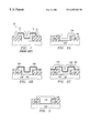
- One proposed way to accomplish this is to switch from the conventional polysilicon-insulator-polysilicon capacitors to metal-insulator-metal (MIM) capacitors, such as the one shown in FIG. 1 .
- MIM metal-insulator-metal
- metals used as the top 12 and/or bottom 14 electrodes are those with low oxygen affinity such as W, Ni, Co, Ir, Ru, and Pt.
- the insulator 16 is a metal oxide using metals that have a high oxygen affinity.
- Exemplary metal oxides include Ta2O5, Nb2O5, Al2O3, Y2O3, HfO2, TiO2, BaO, SrO and the so-called BST (BaxSr1-xTiO3, 0 ⁇ 1). These metal oxides have dielectric constant values ranging from 10 to 1000 (depending on material, microstructure, crystalline phase, and crystal orientation).
- Ta2O5 and BST are considered the most promising capacitor materials for 256 Mbit and 1 Gbit DRAMs.
- Ta2O5 and BST can be deposited through reactions of metal-organic precursors and oxygen and annealed in the O2 or UV-O3 ambient.
- W, Ni and Co are easily oxidized in the O2 ambient at the high temperatures required.
- W oxidizes to form WO3-y which can vaporize and result in a nonuniform dielectric.
- Ta2O5-y can be produced instead of Ta2O5.
- Ta2O5-y is not stociometric and results in reduced capacitance due to leakage.
- Ir, Ru, and Pt have very high oxidation resistance, they are very expensive and difficult to etch.
- a cost-effective method for fabricating MIM capacitors is disclosed herein. After metal deposition, the metal oxide is formed using an oxidation chemistry that includes CO2 and H2. The CO2/H2 gas ratio is controlled for selective oxidation. Thus, the metal is effectively protected from oxidation due to the existence of both H2 and CO2 as strong reduction reagents.
- An advantage of the invention is providing a cost-effective method for fabricating MIM capacitors using a selective metal-oxide deposition.
- FIG. 1 is a cross-sectional diagram of a previously proposed MIM capacitor
- FIGS. 2A-2C are cross-sectional diagrams of a MIM capacitor according to the invention at various stages of fabrication.
- FIG. 3 is a cross-sectional diagram of a MIM capacitor according to the invention having an alternative bottom plate structure.
- SiH4-CO2-H2 and SiH2Cl2-CO2-H2 may be used to form SiO2 using a blanket CVD process.
- a preferred embodiment of the invention uses a CO2/H2 gas ratio in a selective oxidation process to protect the metal electrode during metal-oxide formation. Protection is achieved because H2 and CO are strong reduction reagents.
- the oxidation-reduction reactions are as follows:
- the CO2/H2 ratio depends on the material and selective oxidation temperature, which can be chosen based on thermodynamic calculation. For the case with W as the bottom electrode and TaCl5 as the precursor for a Ta2O5 film, a typical CO2/H2 ratio is 1E-5 to1E-1 at a temperature of 727° C.
- Metal organic precursors and metal chlorides can react with H2O in either a wet hydrogen or a dry CO2/H2 oxidation procedure to form metal oxides.
- H2O a wet hydrogen or a dry CO2/H2 oxidation procedure
- M refers to the underlying metal electrode for which protection from oxidation is desired.
- H2 and/or CO are strong reduction reagents and protect the metal from oxidation.
- the above example uses a Ta-organic precursor or a Ta-chloride, the invention can be easily applied with similar reactions to other metal-organic precursors and metal-chlorides having a strong oxygen affinity such as Nb, Al, Y, Hf, Ba, and Sr.
- the oxygen affinity of Ta, Nb, Al, Y, Hf, Ba, and Sr are stronger than that of W, Ni, and Co. Therefore, under the appropriate process conditions (temperature, gas pressure, ratio, gas flow, etc.) it is possible to oxidize Ta, Nb, Al, Y, Hf, Ba, and/or Sr to form their oxides (Ta2O5, Nb2O5), Al2O3, etc.) such that the oxidation rate of W, Ni, and/or Co is very small. Accordingly, W, Ni, and/or Co may be used for the metal electrodes of a MIM capacitor with oxides of Ta, Nb, Al, Y, Hf, Ba and/or Sr as the capacitor insulator. Alternatively or additionally, metal-nitrides such as TiN, WN, WSiN, or TiSiN may be used for the capacitor electrodes.
- a semiconductor body 102 is processed through the formation of bottom metal electrode 106 .
- metal electrode 106 is in electrical contact (through at least a diffusion barrier 105 ) with semiconductor body 102 and partially extends over dielectric 104 .
- Dielectric 104 is sometimes referred to as an interlevel dielectric (ILD) or a poly-metal dielectric (PMD).
- ILD interlevel dielectric
- PMD poly-metal dielectric
- Dielectric 104 typically comprises silicon dioxide.
- Bottom metal electrode 106 may be formed by conformal metal deposition to a thickness in the range of 100 ⁇ -1000 ⁇ followed by pattern and etch as shown in FIG. 2 A. Alternatively, bottom metal electrode 106 may fill the hole in dielectric 104 as shown in FIG. 3 . In that case, the thickness of bottom metal electrode 106 may be in the range of 1000 ⁇ -10000 ⁇ . In the preferred embodiment, bottom metal electrode 106 comprises W. Alternatively, bottom metal electrode 106 may comprise other metals with low oxygen affinity such as Ni or Co or metal nitrides such as TiN, WN, WSiN, or TiSiN.
- metal-oxide 108 is deposited over bottom metal 106 .
- Metal oxide 108 contains a metal of high oxygen affinity such as Ta, Nb, Al, Y, Hf, Ba or Sr.
- metal-oxide 108 comprises Ta2O5.
- Metal-oxide 108 is deposited used a metal-organic precursor or a metal-chloride and a dry CO2/H2 gas chemistry. The ratio of CO2/H2 is controlled to minimize the oxidation of bottom metal 106 .
- Ta(OC2H5)5 or TaCl5 may be combined with CO2 and H2 to form Ta2O5 with minimal oxidation of bottom metal 106 .
- a typical process condition can be a CO2/H2 ratio between 1E-5 to 1E-1 at a process temperature of 727.
- the range of the ratio and temperature can be chosen based on thermodynamic calculation.
- a typical temperature range is between 400-1000° C.
- the time duration depends on the thickness of the TaO5 film thickness required. The thicker the film, the longer the time needed.
- the thickness of metal oxide 108 may be in the range of 50 ⁇ -300 ⁇ .
- the metal oxide 108 is preferably annealed in either a wet hydrogen oxidation procedure or a dry CO2/H2 oxidation procedure under appropriate conditions to protect the metal electrode 106 from oxidation.
- top metal 110 is deposited as shown in FIG. 2 C.
- top metal 110 also comprises W.
- top metal 110 may comprise other metals with low oxygen affinity such as Ni or Co or metal nitrides such as TiN, WN, WSiN, or TiSiN.
Abstract
A cost-effective method for fabricating MIM capacitors (120). After metal (106) deposition, the metal oxide (108) is formed using an oxidation chemistry that includes CO2 and H2. The CO2/H2 gas ratio is controlled for selective oxidation. Thus, the metal (106) is effectively protected from oxidation due to the existence of both H2 and CO2 as strong reduction reagent.
Description
This application claims priority under 35 USC §119(e)(1) of provisional application number 60/102,223 filed Sep. 29, 1998.
The invention is generally related to the field of forming capacitors in integrated circuits and more specifically to a method of forming metal-insulator-metal capacitors.
As semiconductor devices continue to scale to smaller and smaller dimensions, capacitors used in integrated circuits, such as those used in DRAM storage cells, need higher capacitance/unit area. One proposed way to accomplish this is to switch from the conventional polysilicon-insulator-polysilicon capacitors to metal-insulator-metal (MIM) capacitors, such as the one shown in FIG. 1. In the MIM capacitor 10, metals used as the top 12 and/or bottom 14 electrodes are those with low oxygen affinity such as W, Ni, Co, Ir, Ru, and Pt. The insulator 16 is a metal oxide using metals that have a high oxygen affinity. Exemplary metal oxides include Ta2O5, Nb2O5, Al2O3, Y2O3, HfO2, TiO2, BaO, SrO and the so-called BST (BaxSr1-xTiO3, 0<×<1). These metal oxides have dielectric constant values ranging from 10 to 1000 (depending on material, microstructure, crystalline phase, and crystal orientation).
Currently, Ta2O5 and BST are considered the most promising capacitor materials for 256 Mbit and 1 Gbit DRAMs. Ta2O5 and BST can be deposited through reactions of metal-organic precursors and oxygen and annealed in the O2 or UV-O3 ambient. Unfortunately, due to their low oxidation resistance, W, Ni and Co are easily oxidized in the O2 ambient at the high temperatures required. When trying to deposit Ta2O5 on W, the W oxidizes to form WO3-y which can vaporize and result in a nonuniform dielectric. Moreover, Ta2O5-y can be produced instead of Ta2O5. Ta2O5-y is not stociometric and results in reduced capacitance due to leakage. Although Ir, Ru, and Pt have very high oxidation resistance, they are very expensive and difficult to etch.
One prior art method of selective oxidation for poly-metal gate formation was proposed by Kobayashi et al (Proc. of 15th Conf. Solid State Devices and Material p. 217 (1983)). In this method, a wet hydrogen oxidation procedure was developed to allow the silicon to oxidize while leaving the tungsten unaffected in a post gate-etch oxidation. The method is based on thermodynamic calculations which show that at, for example, 1000° C. and a P(H2O)/P(H2) ratio (partial pressure ratio of H2O and H2) of 1.0e-05, the equilibrium:
prefers the right side of the reaction, i.e., oxidation of Si and
prefers the left side of the reaction, i.e., reduction of WO3 to W. Therefore, under appropriate conditions, it is possible to oxidize silicon again such that the oxidation rate of W will be prevented.
Unfortunately, it is difficult to generate a uniform steam of pure H2O without heavy metal contaminants because it is hard to completely remove heavy metal from the clean and deionized water used in steam generators for semiconductor device manufacturing. It is also dangerous to generate and control a proper H2/H2O gas ratio using a burning process of mixed oxygen and hydrogen under an excessive hydrogen environment.
The above process has been proposed for light thermal oxidation. In the area of non-selective CVD-SiO2, several CO2-H2 gas chemistries have been proposed. One such gas chemistry is SiH4-CO2-H2 and another is SiH2Cl2-CO2-H2. A CO2-H2 gas chemistry has also been used to produce H2O for H2O addition reactions such as 2AlCl3+3H2O→Al2O3+6HCl. In addition, CO gas has been used in metallurgy as a strong reduction reagent of metal oxides for metal production.
A cost-effective method for fabricating MIM capacitors is disclosed herein. After metal deposition, the metal oxide is formed using an oxidation chemistry that includes CO2 and H2. The CO2/H2 gas ratio is controlled for selective oxidation. Thus, the metal is effectively protected from oxidation due to the existence of both H2 and CO2 as strong reduction reagents.
An advantage of the invention is providing a cost-effective method for fabricating MIM capacitors using a selective metal-oxide deposition.
This and other advantages will be apparent to those of ordinary skill in the art having reference to the specification in conjunction with the drawings.
In the drawings:
FIG. 1 is a cross-sectional diagram of a previously proposed MIM capacitor;
FIGS. 2A-2C are cross-sectional diagrams of a MIM capacitor according to the invention at various stages of fabrication; and
FIG. 3 is a cross-sectional diagram of a MIM capacitor according to the invention having an alternative bottom plate structure.
The invention will now be described in conjunction with a process for forming a MIM capacitor. It will be apparent to those of ordinary skill in the art that the benefits of the invention may be applied to other processes requiring metal oxide deposition over exposed metal.
It is known that SiH4-CO2-H2 and SiH2Cl2-CO2-H2 may be used to form SiO2 using a blanket CVD process. A preferred embodiment of the invention uses a CO2/H2 gas ratio in a selective oxidation process to protect the metal electrode during metal-oxide formation. Protection is achieved because H2 and CO are strong reduction reagents. The oxidation-reduction reactions are as follows:
By controlling the CO2/H2 gas ratio, the metal will be effectively protected from oxidation due to the existence of both H2 and CO as strong reduction reagents. The CO2/H2 ratio depends on the material and selective oxidation temperature, which can be chosen based on thermodynamic calculation. For the case with W as the bottom electrode and TaCl5 as the precursor for a Ta2O5 film, a typical CO2/H2 ratio is 1E-5 to1E-1 at a temperature of 727° C.
Metal organic precursors and metal chlorides can react with H2O in either a wet hydrogen or a dry CO2/H2 oxidation procedure to form metal oxides. For example,
Ta(OC2H5)5+H2O→Ta2O5+by-products
In this example, M refers to the underlying metal electrode for which protection from oxidation is desired. H2 and/or CO are strong reduction reagents and protect the metal from oxidation. Although the above example uses a Ta-organic precursor or a Ta-chloride, the invention can be easily applied with similar reactions to other metal-organic precursors and metal-chlorides having a strong oxygen affinity such as Nb, Al, Y, Hf, Ba, and Sr.
Like Si, the oxygen affinity of Ta, Nb, Al, Y, Hf, Ba, and Sr are stronger than that of W, Ni, and Co. Therefore, under the appropriate process conditions (temperature, gas pressure, ratio, gas flow, etc.) it is possible to oxidize Ta, Nb, Al, Y, Hf, Ba, and/or Sr to form their oxides (Ta2O5, Nb2O5), Al2O3, etc.) such that the oxidation rate of W, Ni, and/or Co is very small. Accordingly, W, Ni, and/or Co may be used for the metal electrodes of a MIM capacitor with oxides of Ta, Nb, Al, Y, Hf, Ba and/or Sr as the capacitor insulator. Alternatively or additionally, metal-nitrides such as TiN, WN, WSiN, or TiSiN may be used for the capacitor electrodes.
A process for forming a MIM capacitor according to a preferred embodiment of the invention will now be described with reference to FIGS. 2A-2C. Referring to FIG. 2A, a semiconductor body 102 is processed through the formation of bottom metal electrode 106. In typical DRAM applications, metal electrode 106 is in electrical contact (through at least a diffusion barrier 105) with semiconductor body 102 and partially extends over dielectric 104. Dielectric 104 is sometimes referred to as an interlevel dielectric (ILD) or a poly-metal dielectric (PMD). Dielectric 104 typically comprises silicon dioxide.
Referring to FIG. 2B, metal-oxide 108 is deposited over bottom metal 106. Metal oxide 108 contains a metal of high oxygen affinity such as Ta, Nb, Al, Y, Hf, Ba or Sr. In the preferred embodiment, metal-oxide 108 comprises Ta2O5. Metal-oxide 108 is deposited used a metal-organic precursor or a metal-chloride and a dry CO2/H2 gas chemistry. The ratio of CO2/H2 is controlled to minimize the oxidation of bottom metal 106. For example, Ta(OC2H5)5 or TaCl5 may be combined with CO2 and H2 to form Ta2O5 with minimal oxidation of bottom metal 106. An example is the growth of Ta2O5 with TaCl5 as a precursor and W as the bottom electrode 106. A typical process condition can be a CO2/H2 ratio between 1E-5 to 1E-1 at a process temperature of 727. The range of the ratio and temperature can be chosen based on thermodynamic calculation. A typical temperature range is between 400-1000° C. The time duration depends on the thickness of the TaO5 film thickness required. The thicker the film, the longer the time needed. For Ta2O5, the thickness of metal oxide 108 may be in the range of 50 Å-300 Å.
After metal-oxide 108 deposition, the metal oxide 108 is preferably annealed in either a wet hydrogen oxidation procedure or a dry CO2/H2 oxidation procedure under appropriate conditions to protect the metal electrode 106 from oxidation.
After annealing, the top metal 110 is deposited as shown in FIG. 2C. In the preferred embodiment, top metal 110 also comprises W. Alternatively, top metal 110 may comprise other metals with low oxygen affinity such as Ni or Co or metal nitrides such as TiN, WN, WSiN, or TiSiN.
While this invention has been described with reference to illustrative embodiments, this description is not intended to be construed in a limiting sense. Various modifications and combinations of the illustrative embodiments, as well as other embodiments of the invention, will be apparent to persons skilled in the art upon reference to the description. It is therefore intended that the appended claims encompass any such modifications or embodiments.
Claims (18)
1. A method of forming an integrated circuit, comprising the steps of:
forming a metal layer over a structure;
depositing a metal-oxide layer by selectively oxidizing a metal-bearing precursor in the presence of CO2 and H2 to form the metal-oxide layer over at least a portion of said metal layer while substantially protecting said metal layer from oxidation.
2. The method of claim 1, wherein said metal layer is a capacitor electrode.
3. The method of claim 1, wherein said metal layer comprises tungsten.
4. The method of claim 1, wherein said metal layer comprises nickel.
5. The method of claim 1, wherein said metal layer comprises cobalt.
6. The method of claim 1 wherein said metal layer comprises a metal nitride.
7. The method of claim 1, wherein said metal-oxide layer comprises a material selected from the group consisting of Ta2O5, NB2O5, Al2O3, Y2O3, HfO2, TiO2, BaO, SrO and BST.
8. The method of claim 1, further comprising the step of forming a top metal electrode over said metal oxide layer.
9. The method of claim 1, wherein the metal-bearing precursor is a metal-organic precursor.
10. The method of claim 1 wherein the metal-bearing precursor is a metal-chloride.
11. A method of fabricating a capacitor on an integrated circuit comprising the steps of:
forming a diffusing barrier over a semiconductor body and over a portion of a dielectric formed over the semiconductor body;
forming a first metal electrode over said diffusion barrier;
forming a metal-oxide layer over said first metal electrode by selective oxidation of a metal-bearing precursor, using a chemistry that comprises CO2 and H2 to substantially protect said first metal electrode from oxidation; and
forming a second metal electrode over said metal-oxide layer.
12. The method of claim 11, wherein said first and second metal electrodes comprise tungsten.
13. The method of claim 11, wherein said first and second metal electrodes comprise nickel.
14. The method of claim 11, wherein said first and second metal electrodes comprise cobalt.
15. The method of claim 11, wherein said first and second metal electrodes comprise a metal nitride.
16. The method of claim 11, wherein said metal-oxide layer comprises a material selected from the group consisting of Ta2O5, NB2O5, Al2O3, Y2O3, HfO2 TiO2, BaO, SrO and BST.
17. The method of claim 11, wherein the metal-bearing precursor is a metal-organic precursor.
18. The method of claim 11, wherein the metal-bearing precursor is a metal-chloride.
Priority Applications (1)
| Application Number | Priority Date | Filing Date | Title |
|---|---|---|---|
| US09/363,801 US6207561B1 (en) | 1998-09-29 | 1999-07-29 | Selective oxidation methods for metal oxide deposition on metals in capacitor fabrication |
Applications Claiming Priority (2)
| Application Number | Priority Date | Filing Date | Title |
|---|---|---|---|
| US10222398P | 1998-09-29 | 1998-09-29 | |
| US09/363,801 US6207561B1 (en) | 1998-09-29 | 1999-07-29 | Selective oxidation methods for metal oxide deposition on metals in capacitor fabrication |
Publications (1)
| Publication Number | Publication Date |
|---|---|
| US6207561B1 true US6207561B1 (en) | 2001-03-27 |
Family
ID=22288773
Family Applications (1)
| Application Number | Title | Priority Date | Filing Date |
|---|---|---|---|
| US09/363,801 Expired - Lifetime US6207561B1 (en) | 1998-09-29 | 1999-07-29 | Selective oxidation methods for metal oxide deposition on metals in capacitor fabrication |
Country Status (2)
| Country | Link |
|---|---|
| US (1) | US6207561B1 (en) |
| JP (1) | JP2000114492A (en) |
Cited By (20)
| Publication number | Priority date | Publication date | Assignee | Title |
|---|---|---|---|---|
| US20020024080A1 (en) * | 2000-08-31 | 2002-02-28 | Derderian Garo J. | Capacitor fabrication methods and capacitor constructions |
| US20020074584A1 (en) * | 2000-12-20 | 2002-06-20 | Micron Technology, Inc. | Low leakage MIM capacitor |
| US20020094632A1 (en) * | 2000-08-31 | 2002-07-18 | Agarwal Vishnu K. | Capacitor fabrication methods and capacitor constructions |
| US20020167038A1 (en) * | 2000-08-30 | 2002-11-14 | Jiong-Ping Lu | Novel high-k dielectric materials and processes for manufacturing them |
| US20020190294A1 (en) * | 2001-06-13 | 2002-12-19 | Toshihiro Iizuka | Semiconductor device having a thin film capacitor and method for fabricating the same |
| KR20030002604A (en) * | 2001-06-29 | 2003-01-09 | 주식회사 하이닉스반도체 | A method for forming a metal-insulator-metal capacitor |
| US6555487B1 (en) | 2000-08-31 | 2003-04-29 | Micron Technology, Inc. | Method of selective oxidation conditions for dielectric conditioning |
| US6573150B1 (en) * | 2000-10-10 | 2003-06-03 | Applied Materials, Inc. | Integration of CVD tantalum oxide with titanium nitride and tantalum nitride to form MIM capacitors |
| US6590246B1 (en) * | 2000-02-08 | 2003-07-08 | Micron Technology, Inc. | Structures and methods for improved capacitor cells in integrated circuits |
| US6596595B1 (en) * | 1998-02-26 | 2003-07-22 | Micron Technology, Inc. | Forming a conductive structure in a semiconductor device |
| US20030197215A1 (en) * | 2002-02-05 | 2003-10-23 | International Business Machines Corporation | A dual stacked metal-insulator-metal capacitor and method for making same |
| KR100414733B1 (en) * | 2001-06-29 | 2004-01-13 | 주식회사 하이닉스반도체 | A method for forming a metal-insulator-metal capacitor |
| US20040115880A1 (en) * | 2002-12-11 | 2004-06-17 | Ahn Byoung Kwon | Method for forming capacitor of semiconductor device |
| US20040126981A1 (en) * | 2002-12-31 | 2004-07-01 | Rao Satyavolu S. Papa | MIM capacitors and methods for fabricating same |
| US20040125541A1 (en) * | 2002-12-30 | 2004-07-01 | Hyun-Jin Chung | Capacitor having oxygen diffusion barrier and method for fabricating the same |
| US20050164445A1 (en) * | 2004-01-23 | 2005-07-28 | Taiwan Semiconductor Manufacturing Co., Ltd. | System and method for integration of HfO2 and RTCVD poly-silicon |
| US20050269669A1 (en) * | 2003-07-21 | 2005-12-08 | Mcclure Brent A | Capacitor constructions and methods of forming |
| US20060169885A1 (en) * | 2003-07-03 | 2006-08-03 | Waters Investments Limited | System and method for isotopic signature and mass analysis |
| US20150255581A1 (en) * | 2014-03-06 | 2015-09-10 | Taiwan Semiconductor Manufacturing Company, Ltd. | Semiconductor Devices and Methods of Manufacture Thereof |
| CN110718538A (en) * | 2018-07-13 | 2020-01-21 | 爱思开海力士有限公司 | Semiconductor device and method for manufacturing the same |
Citations (2)
| Publication number | Priority date | Publication date | Assignee | Title |
|---|---|---|---|---|
| US5336638A (en) * | 1991-03-06 | 1994-08-09 | Hitachi, Ltd. | Process for manufacturing semiconductor devices |
| US5561082A (en) * | 1992-07-31 | 1996-10-01 | Kabushiki Kaisha Toshiba | Method for forming an electrode and/or wiring layer by reducing copper oxide or silver oxide |
-
1999
- 1999-07-29 US US09/363,801 patent/US6207561B1/en not_active Expired - Lifetime
- 1999-09-28 JP JP11274037A patent/JP2000114492A/en active Pending
Patent Citations (2)
| Publication number | Priority date | Publication date | Assignee | Title |
|---|---|---|---|---|
| US5336638A (en) * | 1991-03-06 | 1994-08-09 | Hitachi, Ltd. | Process for manufacturing semiconductor devices |
| US5561082A (en) * | 1992-07-31 | 1996-10-01 | Kabushiki Kaisha Toshiba | Method for forming an electrode and/or wiring layer by reducing copper oxide or silver oxide |
Cited By (62)
| Publication number | Priority date | Publication date | Assignee | Title |
|---|---|---|---|---|
| US6596595B1 (en) * | 1998-02-26 | 2003-07-22 | Micron Technology, Inc. | Forming a conductive structure in a semiconductor device |
| US20040094787A1 (en) * | 2000-02-08 | 2004-05-20 | Micron Technology, Inc. | Structures and methods for improved capacitor cells in integrated circuits |
| US7491602B2 (en) | 2000-02-08 | 2009-02-17 | Micron Technology, Inc. | Structures and methods for improved capacitor cells in integrated circuits |
| US6590246B1 (en) * | 2000-02-08 | 2003-07-08 | Micron Technology, Inc. | Structures and methods for improved capacitor cells in integrated circuits |
| US20050167726A1 (en) * | 2000-08-30 | 2005-08-04 | Jiong-Ping Lu | Novel high-k dielectric materials and processes for manufacturing them |
| US8088659B2 (en) | 2000-08-30 | 2012-01-03 | Micron Technology, Inc. | Method of forming capacitors |
| US6861695B2 (en) * | 2000-08-30 | 2005-03-01 | Micron Technology, Inc. | High-k dielectric materials and processes for manufacturing them |
| US20020167038A1 (en) * | 2000-08-30 | 2002-11-14 | Jiong-Ping Lu | Novel high-k dielectric materials and processes for manufacturing them |
| US20100227450A1 (en) * | 2000-08-30 | 2010-09-09 | Micron Technology, Inc. | Novel high-k dielectric materials and processes for manufacturing them |
| US7732852B2 (en) | 2000-08-30 | 2010-06-08 | Micron Technology, Inc. | High-K dielectric materials and processes for manufacturing them |
| US7544987B2 (en) | 2000-08-30 | 2009-06-09 | Micron Technology, Inc. | High-k dielectric materials and processes for manufacturing them |
| US6787429B2 (en) | 2000-08-30 | 2004-09-07 | Micron Technology, Inc. | High-K dielectric materials and processes for manufacturing them |
| US20030153144A1 (en) * | 2000-08-31 | 2003-08-14 | Weimer Ronald A. | Methods of selective oxidation conditions for dielectric conditioning |
| US6555487B1 (en) | 2000-08-31 | 2003-04-29 | Micron Technology, Inc. | Method of selective oxidation conditions for dielectric conditioning |
| US20020024080A1 (en) * | 2000-08-31 | 2002-02-28 | Derderian Garo J. | Capacitor fabrication methods and capacitor constructions |
| US6734531B2 (en) * | 2000-08-31 | 2004-05-11 | Micron Technology, Inc. | Use of selective oxidation conditions for dielectric conditioning |
| US7109542B2 (en) | 2000-08-31 | 2006-09-19 | Micron Technology, Inc. | Capacitor constructions having a conductive layer |
| US7288808B2 (en) * | 2000-08-31 | 2007-10-30 | Micron Technology, Inc. | Capacitor constructions with enhanced surface area |
| US20070178640A1 (en) * | 2000-08-31 | 2007-08-02 | Derderian Garo J | Capacitor fabrication methods and capacitor constructions |
| US7217615B1 (en) | 2000-08-31 | 2007-05-15 | Micron Technology, Inc. | Capacitor fabrication methods including forming a conductive layer |
| US20070007572A1 (en) * | 2000-08-31 | 2007-01-11 | Agarwal Vishnu K | Capacitor fabrication methods and capacitor constructions |
| US6784124B2 (en) * | 2000-08-31 | 2004-08-31 | Micron Technology, Inc. | Methods of selective oxidation conditions for dielectric conditioning |
| US6576979B2 (en) * | 2000-08-31 | 2003-06-10 | Micron Technology, Inc. | Use of selective oxidation conditions for dielectric conditioning |
| US7112503B1 (en) | 2000-08-31 | 2006-09-26 | Micron Technology, Inc. | Enhanced surface area capacitor fabrication methods |
| US20020094632A1 (en) * | 2000-08-31 | 2002-07-18 | Agarwal Vishnu K. | Capacitor fabrication methods and capacitor constructions |
| US6573150B1 (en) * | 2000-10-10 | 2003-06-03 | Applied Materials, Inc. | Integration of CVD tantalum oxide with titanium nitride and tantalum nitride to form MIM capacitors |
| US7435641B2 (en) | 2000-12-20 | 2008-10-14 | Micron Technology, Inc. | Low leakage MIM capacitor |
| US20080057663A1 (en) * | 2000-12-20 | 2008-03-06 | Micron Technology, Inc. | Low leakage mim capacitor |
| US20130285206A1 (en) * | 2000-12-20 | 2013-10-31 | Micron Technology, Inc. | Low leakage mim capacitor |
| US8470665B2 (en) | 2000-12-20 | 2013-06-25 | Micron Technology, Inc. | Low leakage MIM capacitor |
| US20020074584A1 (en) * | 2000-12-20 | 2002-06-20 | Micron Technology, Inc. | Low leakage MIM capacitor |
| US20020192904A1 (en) * | 2000-12-20 | 2002-12-19 | Micron Technology, Inc. | Low leakage MIM capacitor |
| US7378719B2 (en) | 2000-12-20 | 2008-05-27 | Micron Technology, Inc. | Low leakage MIM capacitor |
| US7368343B2 (en) | 2000-12-20 | 2008-05-06 | Micron Technology, Inc. | Low leakage MIM capacitor |
| US20080064179A1 (en) * | 2000-12-20 | 2008-03-13 | Micron Technology, Inc. | Low leakage mim capacitor |
| US8169013B2 (en) | 2001-06-13 | 2012-05-01 | Renesas Electronics Corporation | Metal-insulator-metal (MIM) capacitor having capacitor dielectric material selected from a group consisting of ZRO2, HFO2, (ZRX, HF1-X)O2 (0<x<1), (ZRy, Ti (O<y<1), (Hfz, Ti-z)O2 (O<z<1) and (Zrk, Ti1, Hfm)O2 (O<K, 1, m<1, K+1+m=1) |
| US20020190294A1 (en) * | 2001-06-13 | 2002-12-19 | Toshihiro Iizuka | Semiconductor device having a thin film capacitor and method for fabricating the same |
| DE10226381B4 (en) * | 2001-06-13 | 2015-08-20 | Renesas Electronics Corporation | METHOD FOR PRODUCING A SEMICONDUCTOR DEVICE WITH A THIN FILM CONDENSER |
| US8815678B2 (en) | 2001-06-13 | 2014-08-26 | Renesas Electronics Corporation | Method for fabricating a metal-insulator-metal (MIM) capacitor having capacitor dielectric layer formed by atomic layer deposition (ALD) |
| US20080064147A1 (en) * | 2001-06-13 | 2008-03-13 | Nec Corporation | Method for fabricating a metal-insulator-metal (mim) capacitor having capacitor dielectric layer formed by atomic layer deposition (ald) |
| US20070152256A1 (en) * | 2001-06-13 | 2007-07-05 | Toshihiro Iizuka | Method for fabricating a metal insulator-metal (MIM) capacitor having capacitor dielectric layer formed by atomic layer deposition (ALD) |
| US8212299B2 (en) * | 2001-06-13 | 2012-07-03 | Renesas Electronics Corporation | Semiconductor device having a thin film capacitor of a MIM (metal-insulator-metal) structure |
| KR100414733B1 (en) * | 2001-06-29 | 2004-01-13 | 주식회사 하이닉스반도체 | A method for forming a metal-insulator-metal capacitor |
| KR20030002604A (en) * | 2001-06-29 | 2003-01-09 | 주식회사 하이닉스반도체 | A method for forming a metal-insulator-metal capacitor |
| US20030197215A1 (en) * | 2002-02-05 | 2003-10-23 | International Business Machines Corporation | A dual stacked metal-insulator-metal capacitor and method for making same |
| US20040115880A1 (en) * | 2002-12-11 | 2004-06-17 | Ahn Byoung Kwon | Method for forming capacitor of semiconductor device |
| US6893913B2 (en) | 2002-12-11 | 2005-05-17 | Hynix Semiconductor Inc. | Method for forming capacitor of semiconductor device |
| US20040125541A1 (en) * | 2002-12-30 | 2004-07-01 | Hyun-Jin Chung | Capacitor having oxygen diffusion barrier and method for fabricating the same |
| US6803641B2 (en) | 2002-12-31 | 2004-10-12 | Texas Instruments Incorporated | MIM capacitors and methods for fabricating same |
| US6919233B2 (en) | 2002-12-31 | 2005-07-19 | Texas Instruments Incorporated | MIM capacitors and methods for fabricating same |
| US20040126981A1 (en) * | 2002-12-31 | 2004-07-01 | Rao Satyavolu S. Papa | MIM capacitors and methods for fabricating same |
| US20040124496A1 (en) * | 2002-12-31 | 2004-07-01 | Rao Satyavolu S. Papa | MIM capacitors and methods for fabricating same |
| US20060169885A1 (en) * | 2003-07-03 | 2006-08-03 | Waters Investments Limited | System and method for isotopic signature and mass analysis |
| US7440255B2 (en) | 2003-07-21 | 2008-10-21 | Micron Technology, Inc. | Capacitor constructions and methods of forming |
| US20050269669A1 (en) * | 2003-07-21 | 2005-12-08 | Mcclure Brent A | Capacitor constructions and methods of forming |
| US20050164445A1 (en) * | 2004-01-23 | 2005-07-28 | Taiwan Semiconductor Manufacturing Co., Ltd. | System and method for integration of HfO2 and RTCVD poly-silicon |
| US7037816B2 (en) | 2004-01-23 | 2006-05-02 | Taiwan Semiconductor Manufacturing Company, Ltd. | System and method for integration of HfO2 and RTCVD poly-silicon |
| US20150255581A1 (en) * | 2014-03-06 | 2015-09-10 | Taiwan Semiconductor Manufacturing Company, Ltd. | Semiconductor Devices and Methods of Manufacture Thereof |
| US9818603B2 (en) * | 2014-03-06 | 2017-11-14 | Taiwan Semiconductor Manufacturing Company, Ltd. | Semiconductor devices and methods of manufacture thereof |
| CN110718538A (en) * | 2018-07-13 | 2020-01-21 | 爱思开海力士有限公司 | Semiconductor device and method for manufacturing the same |
| US11855172B2 (en) | 2018-07-13 | 2023-12-26 | SK Hynix Inc. | Semiconductor device and method for fabricating the same |
| CN110718538B (en) * | 2018-07-13 | 2024-02-09 | 爱思开海力士有限公司 | Semiconductor device and method for manufacturing the same |
Also Published As
| Publication number | Publication date |
|---|---|
| JP2000114492A (en) | 2000-04-21 |
Similar Documents
| Publication | Publication Date | Title |
|---|---|---|
| US6207561B1 (en) | Selective oxidation methods for metal oxide deposition on metals in capacitor fabrication | |
| US6858536B2 (en) | Processes to form a metallic film stack | |
| US6740554B2 (en) | Methods to form rhodium-rich oxygen barriers | |
| JP5247059B2 (en) | Method for manufacturing an integrated circuit capacitor using a tantalum pentoxide layer | |
| US5846859A (en) | Method for manufacturing a semiconductor memory device having capacitive storage | |
| US6346746B1 (en) | Capacitor and electrode structures for a semiconductor device | |
| KR100235949B1 (en) | Manufacturing method of capacitor of semiconductor device | |
| US6828190B2 (en) | Method for manufacturing capacitor of semiconductor device having dielectric layer of high dielectric constant | |
| KR100406549B1 (en) | Method for fabricating capacitor having zirconium oxide | |
| US6730616B2 (en) | Versatile plasma processing system for producing oxidation resistant barriers | |
| KR20010027083A (en) | Method of manufacturing a capacitor in a semiconductor device | |
| KR20010027082A (en) | Method of manufacturing a capacitor in a semiconductor device | |
| KR100600333B1 (en) | Method of manufacturing a capacitor in a semiconductor device | |
| KR100361205B1 (en) | Method of manufacturing a capacitor in a semiconductor device | |
| KR20020001373A (en) | Method of manufacturing a capacitor in a semiconductor device | |
| KR100685637B1 (en) | Method of manufacturing a capacitor in a semiconductor device | |
| KR100494342B1 (en) | Method of manufacturing a capacitor in a semiconductor device | |
| KR100671634B1 (en) | Method for Fabricating Capacitor of Semiconductor Device | |
| KR100376257B1 (en) | Method of manufacturing a capacitor in semiconductor device | |
| KR100223893B1 (en) | The manufacturing method of semiconductor memory device | |
| KR20020055251A (en) | Method of manufacturing a capacitor | |
| KR20020050368A (en) | Method of manufacturing a capacitor in a semiconductor device | |
| KR20010016811A (en) | Method of manufacturing a capacitor in a semiconductor device | |
| KR20020055250A (en) | Method of manufacturing a capacitor in semiconductor device | |
| KR19990012240A (en) | Capacitor provided with a platinum group metal electrode and its manufacturing method |
Legal Events
| Date | Code | Title | Description |
|---|---|---|---|
| AS | Assignment |
Owner name: TEXAS INSTRUMENTS INCORPORATED, TEXAS Free format text: ASSIGNMENT OF ASSIGNORS INTEREST;ASSIGNORS:HWANG, MING;TSU, ROBERT;HSU, WEI-YANG;REEL/FRAME:010142/0391;SIGNING DATES FROM 19981002 TO 19981027 |
|
| STCF | Information on status: patent grant |
Free format text: PATENTED CASE |
|
| FEPP | Fee payment procedure |
Free format text: PAYER NUMBER DE-ASSIGNED (ORIGINAL EVENT CODE: RMPN); ENTITY STATUS OF PATENT OWNER: LARGE ENTITY |
|
| FPAY | Fee payment |
Year of fee payment: 4 |
|
| FPAY | Fee payment |
Year of fee payment: 8 |
|
| FPAY | Fee payment |
Year of fee payment: 12 |