US6184745B1 - Reference voltage generating circuit - Google Patents
Reference voltage generating circuit Download PDFInfo
- Publication number
- US6184745B1 US6184745B1 US09/178,476 US17847698A US6184745B1 US 6184745 B1 US6184745 B1 US 6184745B1 US 17847698 A US17847698 A US 17847698A US 6184745 B1 US6184745 B1 US 6184745B1
- Authority
- US
- United States
- Prior art keywords
- reference voltage
- voltage
- pmos transistor
- output node
- power supply
- Prior art date
- Legal status (The legal status is an assumption and is not a legal conclusion. Google has not performed a legal analysis and makes no representation as to the accuracy of the status listed.)
- Expired - Lifetime
Links
Images


Classifications
-
- G—PHYSICS
- G11—INFORMATION STORAGE
- G11C—STATIC STORES
- G11C5/00—Details of stores covered by group G11C11/00
- G11C5/14—Power supply arrangements, e.g. power down, chip selection or deselection, layout of wirings or power grids, or multiple supply levels
-
- G—PHYSICS
- G05—CONTROLLING; REGULATING
- G05F—SYSTEMS FOR REGULATING ELECTRIC OR MAGNETIC VARIABLES
- G05F3/00—Non-retroactive systems for regulating electric variables by using an uncontrolled element, or an uncontrolled combination of elements, such element or such combination having self-regulating properties
- G05F3/02—Regulating voltage or current
- G05F3/08—Regulating voltage or current wherein the variable is DC
- G05F3/10—Regulating voltage or current wherein the variable is DC using uncontrolled devices with non-linear characteristics
- G05F3/16—Regulating voltage or current wherein the variable is DC using uncontrolled devices with non-linear characteristics being semiconductor devices
- G05F3/20—Regulating voltage or current wherein the variable is DC using uncontrolled devices with non-linear characteristics being semiconductor devices using diode- transistor combinations
- G05F3/24—Regulating voltage or current wherein the variable is DC using uncontrolled devices with non-linear characteristics being semiconductor devices using diode- transistor combinations wherein the transistors are of the field-effect type only
- G05F3/242—Regulating voltage or current wherein the variable is DC using uncontrolled devices with non-linear characteristics being semiconductor devices using diode- transistor combinations wherein the transistors are of the field-effect type only with compensation for device parameters, e.g. channel width modulation, threshold voltage, processing, or external variations, e.g. temperature, loading, supply voltage
Definitions
- the present invention relates to a reference voltage generating circuit, and more particularly to a MOS-type reference voltage generating circuit.
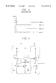
- FIG. 1 illustrates a conventional reference voltage generating circuit using a voltage difference Vgs between a gate and a source of an NMOS transistor.
- First and second PMOS transistors P 11 , P 12 constitute a current mirror and first and second NMOS transistors N 11 , N 12 are respectively connected between each drain of the first and second PMOS transistors P 11 , P 12 and a ground.
- a back-bias voltage Vbb is applied to each substrate of the first and second NMOS transistors N 11 , N 12 for the purpose of effectively diminishing a threshold voltage change, and gates of the first and second NMOS transistors N 11 , N 12 are commonly connected to an output node A.
- each of the PMOS transistors P 11 , P 12 has the identical length and width.
- the NMOS transistors N 11 , N 12 have the same length but a width of the first NMOS transistor N 11 is greater than that of the second NMOS transistor N 12 (W n11 >W n12 ).
- an operation current applied to the output node A from the NMOS transistors N 11 , N 12 may be represented by a following equation (1).
- Iop Vgs ⁇ ( N12 ) - Vgs ⁇ ( N11 ) R1 ( 1 )
- Vgs(N 12 ) denotes a voltage difference between the gate and source of the NMOS transistor N 12 and Vgs(N 11 ) is a voltage difference between the gate and source of the NMOS transistor N 11 .
- each of the currents I n11 , I n12 which are applied to the first and the second NMOS transistors N 11 , N 12 , respectively, may be expressed as follows.
- Vtn denotes a threshold voltage of the NMOS transistors N 11 , N 12
- each of ⁇ 1 , ⁇ 2 which are the process parameters represents a transconductance.
- ⁇ U N ⁇ ⁇ t ox ⁇ ( W L ) ,
- U N is electronic mobility of each of the NMOS transistors
- ⁇ is a dielectric constant
- t ox is a gate oxide thickness
- I op 2 R1 2 ⁇ ⁇ 1 ⁇ ( K - 1 ) 2 ( 5 )
- Vref Vtn + 2 R1 ⁇ ⁇ 2 ⁇ ( 1 - 1 K ) ( 6 )
- the reference voltage Vref since the reference voltage Vref is determined by the threshold voltage Vtn, resistance R 1 , the process parameter ⁇ 2 , and a constant K, the reference voltage Vref may be generated irrespective of any change of a power supply voltage Vcc.
- the threshold voltage Vtn generally has ⁇ 1 mV/° C. of a temperature dependency
- the resistance R of which a gate is formed of a doped polysilicon has +0.01/° C. thereof.
- the electronic mobility U N varies by T - 3 2
- the reference voltage Vref can be generated, regardless of any temperature change.
- the threshold voltage Vtn of the NMOS transistors N 11 , N 12 may vary in accordance with the back-bias voltage Vbb which is applied to the corresponding substrates of the first and second NMOS transistors N 11 , N 12 .
- a bulk of each of the NMOS transistors N 11 , N 12 is connected to a p-type substrate and the p-type substrate is biased at a negative back-bias voltage Vbb which is generated inside a chip device. Accordingly, the back-bias voltage Vbb generates a voltage difference Vsb between the source and the bulk of each of the NMOS transistors N 11 , N 12 , and thus has an effect on the threshold voltage Vtn as a following equation (7).
- Vtn Vtn 0+ ⁇ ⁇ square root over (Vsb) ⁇ (7)
- ⁇ is a body effect factor which has a value of the range between 0.4 to 1.2 according to doping condition
- Vsb is the voltage difference between the source and the bulk of the NMOS transistor.
- FIG. 2 is a graph which illustrates a change of the threshold voltage Vtn in accordance with which the back-bias voltage Vbb varies, and shows that as an absolute value of the back-bias voltage Vbb increases, the threshold voltage Vtn thus correspondingly increases.
- FIG. 3 is a graph illustrating a simulation result which shows a change of the reference voltage Vref with respect to the back-bias voltage Vbb.
- the reference voltage Vref is not considerably affected by the change of the power supply voltage Vcc when the back-bias voltage Vbb is uniformly maintained; however, when the back-bias voltage Vbb changes, the voltage Vref accordingly has a dependency of +178 mV/V.
- the back-bias voltage Vbb is generally equivalent to ⁇ 1 ⁇ 2 of the power supply voltage Vcc
- the absolute value of the back-bias voltage Vbb also increases as the power supply voltage Vcc increases.
- the threshold voltage Vtn increases in accordance therewith and thus the reference voltage Vref consequently increases, which leads to the problem.
- An object of the present invention is to provide a reference voltage generating circuit that substantially obviates at least one of the problems or disadvantages of the conventional art.
- Another object of the present invention is to provide a reference voltage generating circuit that generates an uniform reference voltage regardless of any change of a back-bias voltage by using a voltage difference between a gate and a source of a PMOS transistor.
- a reference voltage generating circuit that includes a reference voltage generating unit for generating a first reference voltage with respect to a power supply voltage, and a level converting unit for converting the first reference voltage supplied from the reference voltage generating unit to a second reference voltage with respect to a ground voltage.
- FIG. 1 is a schematic block diagram illustrating conventional reference voltage generating circuit
- FIG. 2 is a graph illustrating a change of a threshold voltage with respect to a change of a back-bias voltage
- FIG. 3 is a graph illustrating a change of a reference voltage with respect to a change of a back-bias voltage
- FIG. 4 is a schematic block diagram illustrating a first embodiment of a reference voltage generating circuit according to the present invention
- FIG. 5 is a graph wherein a reference voltage to a power supply voltage has been converted to a reference voltage with respect to a ground voltage
- FIG. 6 is a schematic block diagram illustrating a second embodiment of a reference voltage generating circuit according to the present invention.
- FIG. 4 illustrates a reference voltage generating circuit according to a first embodiment of the present invention, which generates a reference voltage, using a voltage difference between a gate and a source of a PMOS transistor.
- the reference voltage generating circuit is provided with a reference voltage generating unit 10 which generates a reference voltage Vref 1 with respect to a power supply voltage Vcc and a level converting unit 20 which converts the reference voltage Vref 1 supplied from the reference voltage generating unit 10 to a reference voltage Vref 2 with respect to a ground voltage Vss.
- the reference voltage generating unit 10 generates the reference voltage Vref 1 with respect to a power supply voltage Vcc, using a pair of PMOS transistors P 1 , P 2 , and constitutes a current mirror circuit with a resistor R 2 and a pair of NMOS transistors N 1 , N 2 .
- the reference voltage generating unit 10 is provided with the PMOS transistor P 1 receiving the power supply voltage Vcc over the resistor R 2 to a source and a bulk (a bias of an N-Well) thereof, the PMOS transistor P 2 having a source and a bulk, both of which receive the power supply voltage Vcc, and a gate connected with a gate of the PMOS transistor P 1 , and the pair of NMOS transistors N 1 , N 2 , each being connected between the drain of the corresponding PMOS transistor P 1 , P 2 and the ground for thus being used as a current mirror circuit.
- a back-bias voltage Vbb is applied to each bulk of the NMOS transistors N 1 , N 2 , the NMOS transistors N 1 , N 2 operate at an active load, and a voltage difference Vgs of each of the PMOS transistors is identical to each other.
- the level converting unit 20 is comprised of a pair of PMOS transistors P 3 , P 4 which are serially connected with each other between the power supply voltage Vcc and the ground.
- a source of the PMOS transistor P 3 is connected with a bulk thereof and a gate thereof is commonly connected with the drain and gate of the PMOS transistor P 2 of the reference voltage generating unit 10 .
- the PMOS transistor P 4 is a diode-type transistor.
- each bulk of the PMOS transistors P 1 , P 2 that is the bias of the N-Well, is connected with the corresponding source thereof, for thereby eliminating a body effect by not making any voltage difference between the source and bulk of the PMOS transistor.
- an operation current I op which flows towards an output node C by the current mirror operation of the NMOS transistors N 1 , N 2 can be represented as a following equation (8).
- I op Vgs ⁇ ( P1 ) - Vgs ⁇ ( P2 ) R2 ( 8 )
- Vcc - Vref1 Vtp + 2 R1 ⁇ ⁇ p2 ⁇ ( 1 - 1 K ) ( 9 )
- Vtp and ⁇ p2 denote a threshold voltage of the PMOS transistor and a transconductance of the PMOS transistor P 2 , respectively.
- the reference voltage to the power supply voltage Vcc maintains a uniform voltage value (Vcc ⁇ Vref 1 ), and though the threshold voltage Vtn of the NMOS transistor is increased by the equation (8), the voltage value (Vcc ⁇ Vref 1 ) still maintains a uniform value, but only a drain voltage of the NMOS transistor N 2 is changed.
- the reference voltage Vref 1 to the power supply voltage Vcc which is supplied from the reference voltage generating unit 10 varies to the reference voltage Vref 2 with respect to the ground voltage Vss in the reference voltage converting unit 20 .
- FIG. 6 illustrates a second embodiment of a reference voltage generating circuit according to the present invention, in which the output node C of the reference voltage generating unit 10 illustrated in FIG. 4 is connected with a level converting unit 30 .
- the level converting unit 30 is comprised of a PMOS transistor P 5 connected between a power supply voltage Vcc and an output node E, and three diode-type PMOS transistors P 6 -P 8 which are connected between the output node E and the ground. At this time, a source of each of the diode-type PMOS transistors P 6 -P 8 is connected with a corresponding bulk and a gate thereof is connected with a drain.
- the diode-type PMOS transistors P 6 -P 8 have the same W/L(width/length).
- the reference voltage Vref 1 with respect to the power supply voltage Vcc changes to the reference voltage Vref 3 with respect to the ground voltage Vss, and the size of the reference voltage Vref 3 is about three times as large as that of the reference voltage Vref 2 .
- the number of the diode-type PMOS transistors may be adjusted by the user.
- the reference voltage generating circuit of the present invention which generates the reference voltage by using the voltage difference of the PMOS transistor has an effect of generating a uniform reference voltage, irrespective of the change of the back-bias voltage Vbb.
Landscapes
- Engineering & Computer Science (AREA)
- Microelectronics & Electronic Packaging (AREA)
- Physics & Mathematics (AREA)
- Nonlinear Science (AREA)
- Electromagnetism (AREA)
- General Physics & Mathematics (AREA)
- Radar, Positioning & Navigation (AREA)
- Automation & Control Theory (AREA)
- Power Engineering (AREA)
- Control Of Electrical Variables (AREA)
- Dram (AREA)
Abstract
Description


Claims (16)
Applications Claiming Priority (2)
| Application Number | Priority Date | Filing Date | Title |
|---|---|---|---|
| KR1019970065207A KR19990047008A (en) | 1997-12-02 | 1997-12-02 | Reference voltage generation circuit insensitive to changes in external conditions |
| KR97-65207 | 1997-12-02 |
Publications (1)
| Publication Number | Publication Date |
|---|---|
| US6184745B1 true US6184745B1 (en) | 2001-02-06 |
Family
ID=19526219
Family Applications (1)
| Application Number | Title | Priority Date | Filing Date |
|---|---|---|---|
| US09/178,476 Expired - Lifetime US6184745B1 (en) | 1997-12-02 | 1998-10-26 | Reference voltage generating circuit |
Country Status (2)
| Country | Link |
|---|---|
| US (1) | US6184745B1 (en) |
| KR (1) | KR19990047008A (en) |
Cited By (13)
| Publication number | Priority date | Publication date | Assignee | Title |
|---|---|---|---|---|
| US6469572B1 (en) * | 2001-03-28 | 2002-10-22 | Intel Corporation | Forward body bias generation circuits based on diode clamps |
| US6734719B2 (en) * | 2001-09-13 | 2004-05-11 | Kabushiki Kaisha Toshiba | Constant voltage generation circuit and semiconductor memory device |
| US20040164790A1 (en) * | 2003-02-24 | 2004-08-26 | Samsung Electronics Co., Ltd. | Bias circuit having a start-up circuit |
| US20050062518A1 (en) * | 2002-10-07 | 2005-03-24 | Hynix Semiconductor Inc. | Boosting voltage control circuit |
| US20050179486A1 (en) * | 2003-04-17 | 2005-08-18 | Hibourahima Camara | Reference current generation system |
| US20070146061A1 (en) * | 2005-09-30 | 2007-06-28 | Texas Instruments Deutschland Gmbh | Cmos reference voltage source |
| US20090153197A1 (en) * | 2007-12-17 | 2009-06-18 | Premier Image Technology(China) Ltd. | Method of transmitting audio and video signals using one connector and electronic device using same |
| US20100188143A1 (en) * | 2009-01-23 | 2010-07-29 | Sony Corporation | Bias circuit, and gm-C filter circuit and semiconductor integrated circuit each including the same |
| US20110278936A1 (en) * | 2010-05-13 | 2011-11-17 | Texas Instruments Incorporated | Low dropout regulator with multiplexed power supplies |
| US20120056609A1 (en) * | 2010-09-07 | 2012-03-08 | Kabushiki Kaisha Toshiba | Reference current generation circuit |
| US8760216B2 (en) | 2009-06-09 | 2014-06-24 | Analog Devices, Inc. | Reference voltage generators for integrated circuits |
| CN115113676A (en) * | 2021-03-18 | 2022-09-27 | 纮康科技股份有限公司 | Reference circuit with temperature compensation function |
| US20220342436A1 (en) * | 2021-04-22 | 2022-10-27 | Taiwan Semiconductor Manufacturing Company Ltd. | Bias generating devices and methods for generating bias |
Families Citing this family (1)
| Publication number | Priority date | Publication date | Assignee | Title |
|---|---|---|---|---|
| US11971736B2 (en) * | 2022-02-16 | 2024-04-30 | Sandisk Technologies Llc | Current mirror circuits |
Citations (8)
| Publication number | Priority date | Publication date | Assignee | Title |
|---|---|---|---|---|
| US4935690A (en) * | 1988-10-31 | 1990-06-19 | Teledyne Industries, Inc. | CMOS compatible bandgap voltage reference |
| US5077518A (en) * | 1990-09-29 | 1991-12-31 | Samsung Electronics Co., Ltd. | Source voltage control circuit |
| US5173656A (en) * | 1990-04-27 | 1992-12-22 | U.S. Philips Corp. | Reference generator for generating a reference voltage and a reference current |
| US5204612A (en) * | 1990-10-29 | 1993-04-20 | Eurosil Electronic Gmbh | Current source circuit |
| US5448159A (en) * | 1994-05-12 | 1995-09-05 | Matsushita Electronics Corporation | Reference voltage generator |
| US5881015A (en) * | 1997-03-22 | 1999-03-09 | Lg Semicon Co., Ltd. | Internal constant voltage control circuit for memory device |
| US5917765A (en) * | 1997-03-27 | 1999-06-29 | Mitsubishi Denki Kabushiki Kaisha | Semiconductor memory device capable of burn in mode operation |
| US6005434A (en) * | 1995-03-31 | 1999-12-21 | Mitsubishi Denki Kabushiki Kaisha | Substrate potential generation circuit that can suppress variation of output voltage with respect to change in external power supply voltage and environment temperature |
-
1997
- 1997-12-02 KR KR1019970065207A patent/KR19990047008A/en not_active Ceased
-
1998
- 1998-10-26 US US09/178,476 patent/US6184745B1/en not_active Expired - Lifetime
Patent Citations (8)
| Publication number | Priority date | Publication date | Assignee | Title |
|---|---|---|---|---|
| US4935690A (en) * | 1988-10-31 | 1990-06-19 | Teledyne Industries, Inc. | CMOS compatible bandgap voltage reference |
| US5173656A (en) * | 1990-04-27 | 1992-12-22 | U.S. Philips Corp. | Reference generator for generating a reference voltage and a reference current |
| US5077518A (en) * | 1990-09-29 | 1991-12-31 | Samsung Electronics Co., Ltd. | Source voltage control circuit |
| US5204612A (en) * | 1990-10-29 | 1993-04-20 | Eurosil Electronic Gmbh | Current source circuit |
| US5448159A (en) * | 1994-05-12 | 1995-09-05 | Matsushita Electronics Corporation | Reference voltage generator |
| US6005434A (en) * | 1995-03-31 | 1999-12-21 | Mitsubishi Denki Kabushiki Kaisha | Substrate potential generation circuit that can suppress variation of output voltage with respect to change in external power supply voltage and environment temperature |
| US5881015A (en) * | 1997-03-22 | 1999-03-09 | Lg Semicon Co., Ltd. | Internal constant voltage control circuit for memory device |
| US5917765A (en) * | 1997-03-27 | 1999-06-29 | Mitsubishi Denki Kabushiki Kaisha | Semiconductor memory device capable of burn in mode operation |
Non-Patent Citations (1)
| Title |
|---|
| Hoi-Jun Yoo et al.; "A Precision CMOS Voltage Reference with Enhanced Stability for the Application to Advanced VLSI's"; 1993 IEEE; pp. 1318-1321. |
Cited By (20)
| Publication number | Priority date | Publication date | Assignee | Title |
|---|---|---|---|---|
| US6469572B1 (en) * | 2001-03-28 | 2002-10-22 | Intel Corporation | Forward body bias generation circuits based on diode clamps |
| US6734719B2 (en) * | 2001-09-13 | 2004-05-11 | Kabushiki Kaisha Toshiba | Constant voltage generation circuit and semiconductor memory device |
| US20050062518A1 (en) * | 2002-10-07 | 2005-03-24 | Hynix Semiconductor Inc. | Boosting voltage control circuit |
| US7123078B2 (en) * | 2002-10-07 | 2006-10-17 | Hynix Semiconductor Inc. | Boosting voltage control circuit |
| US20040164790A1 (en) * | 2003-02-24 | 2004-08-26 | Samsung Electronics Co., Ltd. | Bias circuit having a start-up circuit |
| US20050179486A1 (en) * | 2003-04-17 | 2005-08-18 | Hibourahima Camara | Reference current generation system |
| US7132821B2 (en) * | 2003-04-17 | 2006-11-07 | International Business Machines Corporation | Reference current generation system |
| US20070146061A1 (en) * | 2005-09-30 | 2007-06-28 | Texas Instruments Deutschland Gmbh | Cmos reference voltage source |
| US8203364B2 (en) * | 2007-12-17 | 2012-06-19 | Premier Image Technology(China) Ltd. | Method of transmitting audio and video signals using one connector and electronic device using same |
| US20090153197A1 (en) * | 2007-12-17 | 2009-06-18 | Premier Image Technology(China) Ltd. | Method of transmitting audio and video signals using one connector and electronic device using same |
| US20100188143A1 (en) * | 2009-01-23 | 2010-07-29 | Sony Corporation | Bias circuit, and gm-C filter circuit and semiconductor integrated circuit each including the same |
| US8760216B2 (en) | 2009-06-09 | 2014-06-24 | Analog Devices, Inc. | Reference voltage generators for integrated circuits |
| US8531056B2 (en) * | 2010-05-13 | 2013-09-10 | Texas Instruments Incorporated | Low dropout regulator with multiplexed power supplies |
| US20110278936A1 (en) * | 2010-05-13 | 2011-11-17 | Texas Instruments Incorporated | Low dropout regulator with multiplexed power supplies |
| US20120056609A1 (en) * | 2010-09-07 | 2012-03-08 | Kabushiki Kaisha Toshiba | Reference current generation circuit |
| US8760143B2 (en) * | 2010-09-07 | 2014-06-24 | Kabushiki Kaisha Toshiba | Reference current generation circuit |
| CN115113676A (en) * | 2021-03-18 | 2022-09-27 | 纮康科技股份有限公司 | Reference circuit with temperature compensation function |
| CN115113676B (en) * | 2021-03-18 | 2024-03-01 | 纮康科技股份有限公司 | Reference circuit with temperature compensation |
| US20220342436A1 (en) * | 2021-04-22 | 2022-10-27 | Taiwan Semiconductor Manufacturing Company Ltd. | Bias generating devices and methods for generating bias |
| US11953927B2 (en) * | 2021-04-22 | 2024-04-09 | Taiwan Semiconductor Manufacturing Company Ltd. | Bias generating devices and methods for generating bias |
Also Published As
| Publication number | Publication date |
|---|---|
| KR19990047008A (en) | 1999-07-05 |
Similar Documents
| Publication | Publication Date | Title |
|---|---|---|
| US5900772A (en) | Bandgap reference circuit and method | |
| US6459326B2 (en) | Method for generating a substantially temperature independent current and device allowing implementation of the same | |
| US8441309B2 (en) | Temperature independent reference circuit | |
| US5825695A (en) | Semiconductor device for reference voltage | |
| US5434534A (en) | CMOS voltage reference circuit | |
| US20100156386A1 (en) | Reference voltage circuit | |
| US6184745B1 (en) | Reference voltage generating circuit | |
| EP0573240A2 (en) | Reference voltage generator | |
| US7208998B2 (en) | Bias circuit for high-swing cascode current mirrors | |
| US20080180070A1 (en) | Reference voltage generation circuit | |
| US8026756B2 (en) | Bandgap voltage reference circuit | |
| US6188270B1 (en) | Low-voltage reference circuit | |
| KR100604462B1 (en) | ?? reference voltage for extremely low power supply | |
| KR100253645B1 (en) | Reference voltage generating circuit | |
| US7589580B2 (en) | Reference current generating method and current reference circuit | |
| US6388507B1 (en) | Voltage to current converter with variation-free MOS resistor | |
| US6724243B2 (en) | Bias circuit with voltage and temperature stable operating point | |
| US8067975B2 (en) | MOS resistor with second or higher order compensation | |
| US6680605B2 (en) | Single-seed wide-swing current mirror | |
| US20240321878A1 (en) | Reference Voltage Circuit | |
| US20020109490A1 (en) | Reference current source having MOS transistors | |
| US5627456A (en) | All FET fully integrated current reference circuit | |
| JP3024645B1 (en) | Constant voltage generator | |
| JPH05250050A (en) | Reference voltage generating circuit | |
| JPH11134051A (en) | Reference voltage circuit |
Legal Events
| Date | Code | Title | Description |
|---|---|---|---|
| AS | Assignment |
Owner name: LG SEMICON CO., LTD, KOREA, REPUBLIC OF Free format text: ASSIGNMENT OF ASSIGNORS INTEREST;ASSIGNOR:KIM, TAE-HOON;REEL/FRAME:009542/0199 Effective date: 19981004 |
|
| AS | Assignment |
Owner name: HYUNDAI ELECTRONICS INDUSTRIES, CO., LTD., KOREA, Free format text: MERGER;ASSIGNOR:LG SEMICON CO., LTD.;REEL/FRAME:010951/0606 Effective date: 19991020 |
|
| FEPP | Fee payment procedure |
Free format text: PAYOR NUMBER ASSIGNED (ORIGINAL EVENT CODE: ASPN); ENTITY STATUS OF PATENT OWNER: LARGE ENTITY |
|
| STCF | Information on status: patent grant |
Free format text: PATENTED CASE |
|
| FPAY | Fee payment |
Year of fee payment: 4 |
|
| AS | Assignment |
Owner name: HYNIX SEMICONDUCTOR INC., KOREA, REPUBLIC OF Free format text: CHANGE OF NAME;ASSIGNOR:HYUNDAI ELECTRONICS INDUSTRIES CO., LTD.;REEL/FRAME:015242/0899 Effective date: 20010329 |
|
| AS | Assignment |
Owner name: MAGNACHIP SEMICONDUCTOR, LTD., KOREA, REPUBLIC OF Free format text: ASSIGNMENT OF ASSIGNORS INTEREST;ASSIGNOR:HYNIX SEMICONDUCTOR, INC.;REEL/FRAME:016216/0649 Effective date: 20041004 |
|
| AS | Assignment |
Owner name: U.S. BANK NATIONAL ASSOCIATION, AS COLLATERAL TRUS Free format text: SECURITY INTEREST;ASSIGNOR:MAGNACHIP SEMICONDUCTOR, LTD.;REEL/FRAME:016470/0530 Effective date: 20041223 Owner name: U.S. BANK NATIONAL ASSOCIATION, AS COLLATERAL TRUSTEE, NEW YORK Free format text: SECURITY INTEREST;ASSIGNOR:MAGNACHIP SEMICONDUCTOR, LTD.;REEL/FRAME:016470/0530 Effective date: 20041223 |
|
| FPAY | Fee payment |
Year of fee payment: 8 |
|
| FEPP | Fee payment procedure |
Free format text: PAYER NUMBER DE-ASSIGNED (ORIGINAL EVENT CODE: RMPN); ENTITY STATUS OF PATENT OWNER: LARGE ENTITY Free format text: PAYOR NUMBER ASSIGNED (ORIGINAL EVENT CODE: ASPN); ENTITY STATUS OF PATENT OWNER: LARGE ENTITY |
|
| AS | Assignment |
Owner name: MAGNACHIP SEMICONDUCTOR LTD.,KOREA, DEMOCRATIC PEO Free format text: RELEASE BY SECURED PARTY;ASSIGNOR:U.S. BANK NATIONAL ASSOCIATION;REEL/FRAME:024563/0807 Effective date: 20100527 Owner name: MAGNACHIP SEMICONDUCTOR LTD., KOREA, DEMOCRATIC PEOPLE'S REPUBLIC OF Free format text: RELEASE BY SECURED PARTY;ASSIGNOR:U.S. BANK NATIONAL ASSOCIATION;REEL/FRAME:024563/0807 Effective date: 20100527 |
|
| FPAY | Fee payment |
Year of fee payment: 12 |
|
| AS | Assignment |
Owner name: MAGNACHIP SEMICONDUCTOR LTD., KOREA, REPUBLIC OF Free format text: CORRECTIVE ASSIGNMENT TO CORRECT THE RECEIVING PARTY ADDRESS PREVIOUSLY RECORDED AT REEL: 024563 FRAME: 0807. ASSIGNOR(S) HEREBY CONFIRMS THE RELEASE BY SECURED PARTY;ASSIGNOR:US BANK NATIONAL ASSOCIATION;REEL/FRAME:034469/0001 Effective date: 20100527 |