US6177894B1 - Evaluation system and method for AD converter - Google Patents
Evaluation system and method for AD converter Download PDFInfo
- Publication number
- US6177894B1 US6177894B1 US09/183,644 US18364498A US6177894B1 US 6177894 B1 US6177894 B1 US 6177894B1 US 18364498 A US18364498 A US 18364498A US 6177894 B1 US6177894 B1 US 6177894B1
- Authority
- US
- United States
- Prior art keywords
- signal
- analog
- digital
- amplitude
- transform
- Prior art date
- Legal status (The legal status is an assumption and is not a legal conclusion. Google has not performed a legal analysis and makes no representation as to the accuracy of the status listed.)
- Expired - Lifetime
Links
- 238000000034 method Methods 0.000 title claims description 43
- 238000011156 evaluation Methods 0.000 title abstract description 14
- 238000012360 testing method Methods 0.000 claims abstract description 55
- 230000015654 memory Effects 0.000 claims description 67
- 238000004364 calculation method Methods 0.000 claims description 44
- 238000001914 filtration Methods 0.000 claims description 12
- 125000004122 cyclic group Chemical group 0.000 claims description 6
- 238000012952 Resampling Methods 0.000 claims 11
- 230000001131 transforming effect Effects 0.000 claims 2
- 238000006243 chemical reaction Methods 0.000 abstract description 8
- 238000013459 approach Methods 0.000 description 42
- 238000013139 quantization Methods 0.000 description 29
- 238000012545 processing Methods 0.000 description 17
- 230000006870 function Effects 0.000 description 16
- 238000007792 addition Methods 0.000 description 14
- 230000004044 response Effects 0.000 description 12
- 238000005070 sampling Methods 0.000 description 12
- 238000001228 spectrum Methods 0.000 description 10
- 230000007704 transition Effects 0.000 description 4
- 230000008859 change Effects 0.000 description 3
- 238000007796 conventional method Methods 0.000 description 3
- 230000007423 decrease Effects 0.000 description 3
- 230000007547 defect Effects 0.000 description 3
- 238000001514 detection method Methods 0.000 description 3
- 230000000737 periodic effect Effects 0.000 description 3
- 230000003068 static effect Effects 0.000 description 3
- 238000004422 calculation algorithm Methods 0.000 description 2
- 238000009826 distribution Methods 0.000 description 2
- 230000000694 effects Effects 0.000 description 2
- 238000010606 normalization Methods 0.000 description 2
- 230000009467 reduction Effects 0.000 description 2
- 239000004065 semiconductor Substances 0.000 description 2
- 238000004088 simulation Methods 0.000 description 2
- 238000013519 translation Methods 0.000 description 2
- 235000008733 Citrus aurantifolia Nutrition 0.000 description 1
- 241001036794 Microsorum maximum Species 0.000 description 1
- 235000011941 Tilia x europaea Nutrition 0.000 description 1
- 238000010420 art technique Methods 0.000 description 1
- 230000008901 benefit Effects 0.000 description 1
- 230000001427 coherent effect Effects 0.000 description 1
- 230000000052 comparative effect Effects 0.000 description 1
- 238000013479 data entry Methods 0.000 description 1
- 230000003247 decreasing effect Effects 0.000 description 1
- 230000003111 delayed effect Effects 0.000 description 1
- 238000010586 diagram Methods 0.000 description 1
- 230000010354 integration Effects 0.000 description 1
- 239000004571 lime Substances 0.000 description 1
- 238000012986 modification Methods 0.000 description 1
- 230000004048 modification Effects 0.000 description 1
- 238000009828 non-uniform distribution Methods 0.000 description 1
- 238000011056 performance test Methods 0.000 description 1
- 230000008569 process Effects 0.000 description 1
- 230000000717 retained effect Effects 0.000 description 1
- 230000035945 sensitivity Effects 0.000 description 1
- 239000007787 solid Substances 0.000 description 1
- 238000012384 transportation and delivery Methods 0.000 description 1
Images


Classifications
-
- H—ELECTRICITY
- H03—ELECTRONIC CIRCUITRY
- H03M—CODING; DECODING; CODE CONVERSION IN GENERAL
- H03M1/00—Analogue/digital conversion; Digital/analogue conversion
- H03M1/10—Calibration or testing
- H03M1/1071—Measuring or testing
- H03M1/1085—Measuring or testing using domain transforms, e.g. Fast Fourier Transform
-
- H—ELECTRICITY
- H03—ELECTRONIC CIRCUITRY
- H03M—CODING; DECODING; CODE CONVERSION IN GENERAL
- H03M1/00—Analogue/digital conversion; Digital/analogue conversion
- H03M1/12—Analogue/digital converters
Definitions
- the invention relates to a performance evaluation system and method for evaluating the effective number of bits and the differential non-linearity of an analog-digital converter (ADC) which converts an analog signal into a digital signal and which is implemented by a single semiconductor integrated circuit or a combination of a plurality of semiconductor integrated circuits.
- ADC analog-digital converter
- An approach to evaluate ADC's is categorized into a static and a dynamic characteristic evaluation technique.
- a precisely defined d.c. voltage is applied to an ADC, which is a device under test (DUT), and a response from the ADC is observed in order to estimate “a difference between the transition voltage of an actual ADC and the transition voltage of an ideal ADC” in a computer or like means based on the differential nonlinearity, hereafter referred to as DNL.
- DNL The differential nonlinearity or DNL is obtained by the comparison of a difference in the upper limit amplitude of the analog signal (actual step size) as adjacent quantized codes are delivered from the ADC against an ideal step size which corresponds to 1 LSB, and enables a localized fault which depends on a particular code to be detected.
- DNL for ADC is defined as follows:
- a periodic signal is applied to an ADC under test, a response from the ADC is observed, and “a difference between the transitional voltage of an actual ADC and the transition voltage of an ideal ADC” is; estimated as in a computer.
- This technique has an advantage that a characteristic which closely approximates an actual operation of the ADC, which is under test, can be estimated.
- Dynamic characteristic evaluation techniques which utilize a sine wave (sinusoidal wave) as an input signal include a histogram approach, an FFT approach and a curve fitting approach mentioned below.
- a sine wave signal from a sine wave generator 11 is applied to an ADC 14 under test, as shown in FIG. 1 A.
- a histogram for respective codes is obtained by a histogram analyzer 17 .
- a DNL estimator 18 determines a difference between the histogram for the actual ADC and the histogram of an ideal ADC, and divided by the histogram of the ideal ADC, thus estimating the DNL.
- the normalization of the difference in the histograms by the histogram of the ideal ADC accounts for a non-uniform distribution of the sine wave histogram.
- the relative number of samples for an output from a 6 bits ADC will be as shown in FIG. 1B where the total number of samples is equal to 1024, and the resulting DNL will be obtained as shown in FIG. 1 C.
- a digital signal representing the response of the ADC 14 under test is Fourier transformed as by FFT (fast Fourier transform), and is separated in the frequency domain into a signal (namely, a frequency spectrum of the sine wave applied) and noises (namely, a spectrum of quantization noises or a sum of spectra other than the frequency of the sine wave applied), thus determining a signal-to-noise ratio (SNR).
- FFT fast Fourier transform
- a sine wave signal from a sine wave generator 11 is passed through a low pass filter 12 to eliminate unwanted components therefrom before it is fed to a sample-and-hold circuit 13 where the sine wave signal is sampled periodically and held therein for feeding an ADC 14 under test.
- a response output from the ADC 14 is fed to an FFT unit 15 where it is transformed into a signal in the frequency domain, which is then fed to an SNR estimator 16 .
- the SNR estimator 16 determines the signal-to-noise ratio SNR by dividing the sine wave signal component G SS (f 0 ) by the noise component ⁇ f G nn (f) where f ⁇ f 0 .
- ENOB SNR ⁇ [ dB ] - 1.76 6.02 ⁇ [ bits ] ( 2 )
- the frequency dependency of ENOB can be determined.
- the estimated value of DNL remains little unchanged if the internal noise of the ADC is high or low.
- the influence of the internal noise of the AE)C upon the performance of the ADC cannot be exactly estimated (Ginetti, 1991). Accordingly, the histogram approach cannot be applied for the evaluation of the performance of multi-bit ADC with a high accuracy.
- the ADC converts an analog signal into a digital output code in accordance with the amplitude of the input signal. If the Fourier transform of the output signal is used in evaluating the conversion characteristic of ADC, non-idealities which are localized in individual output codes cannot be separated. This is because defects present within different codes are added together as noises to the rms error. Thus if there is no correlation between the defects and if different codes are influenced by them, these defects will be evaluated as “part of noises which coherently influence the same code.” As a consequence, there is a likelihood that the effective number of effective bits may be underestimated. (See, Robert E.
- the square error does not approach a given value if the calculation of the square error is repeated while changing the parameter of the sine wave. Thus, the error diverges rather than converges.
- the variance of the frequency estimate is proportional to 1/N 3 , a sufficiently great number of samples, in excess of 4096 samples, are necessary to suppress the variance.
- the effective number of bits which can be estimated by this approach corresponds again to a mean value determined over the entire output codes. As a consequence, an analysis of individual factors such as harmonic distortion, noise or aperture jitter which causes a reduction in the effective number of bits is prohibited.
- the histogram approach determines a probability density function by an approximation of a mean value of the histogram of the input sine wave. Accordingly, the DNL or the effective number of bits estimated according to any technique represents a mean value rather than an instantaneous value. As a consequence, it is difficult to estimate independently factors of a compounded fault.
- a relationship other than an integral multiple must be established between the frequency of th(e input sine wave and the sampling frequency of the ADC. For this reason, an arbitrary frequency cannot be selected as the testing frequency.
- a very increased number of samples are required for any technique chosen. Assuming a number of samples equal to 512, the volume of computation needed is as follows:
- a system according to the invention comprises instantaneous amplitude calculation means and digital moving differentiator means.
- the Fourier transform or the curve fitting approach represents a root-mean-square estimator, which requires an increased number of samples in order for the effective number of bits to be estimated with a high accuracy. In addition, a very long time interval is required to determine the probability density function of the sine wave accurately. Accordingly, the Fourier transform approach or the combination of the curve fitting approach and the histogram approach cannot achieve the first, the second and the third object mentioned above. To accomplish these objects, new means is required which can separate non-idealities which are localized in the respective output codes from the ADC. In this respect, in accordance with the invention, instantaneous amplitude calculation means 21 which receives a digital signal comprising output codes from the ADC 14 as an input is used, as shown in FIG. 3 .
- a combination of Fourier transform means and SNR estimator has been used to estimate a mean effective number of bits of a ADC under test indirectly.
- the combination of the Fourier transform means and the SNR estimator is replaced by a combination of Hilbert pair resampler 19 , instantaneous amplitude calculation means 21 , interleaver means 20 , digital moving differentiator means 22 and local maximum or maximum detecting means (peak finder) 23 .
- a sine wave from a sine wave generator 11 is applied to an ADC 14 under test, as shown in FIG. 3, and an instantaneous amplitude of the output from the ADC 14 is calculated by instantaneous amplitude calculator 21 while the Hilbert pair resampler 19 resamples a cosine wave and a sine wave which corresponds to a Hilbert transform pair of the cosine wave output from the ADC 14 .
- the instantaneous amplitude and a known amplitude of the input sine wave are fed to interleaver means 20 where an interleaved signal is formed and is then processed by moving differentiator means 22 .
- Peak finder means 23 determines a maximum value of the absolute amplitude from the differentiator 22 , thereby allowing an instantaneous effective number of bits to be determined therefrom.
- the interleaved signal from the interleaver means 20 is subject to a first stage transform in a wavelet transform means 46 , and a maximum value of the absolute amplitude of the transform output from the first stage is detected by the peak finder means 23 , allowing the instantaneous effective number of bits to be determined therefrom.
- the instantaneous amplitude from the instantaneous amplitude calculation means 21 is fed to digital moving differentiator means 22 ′, and a maximum value of the absolute magnitude of the moving difference output is detected by peak finder means 23 ′, as shown in FIG. 3, thus determining an instantaneous DNL.
- the output from the first stage wavelet transform may be fed to wavelet transform second stage 46 ′ where the output is oversampled to perform another stage of wavelet transform, thus deriving a second stage output from the wavelet transform.
- a maximum value of the absolute magnitude may be determined by peak finder means 23 ′, thus determining an instantaneous DNL.
- Non-idealities which are localized in the respective output codes from an ADC under test cannot be directly determined with the FFT approach or the curve fitting approach.
- a digital signal comprising output codes from the ADC is; subject to a Fourier transform, and a line spectrum which corresponds to an ideal sine wave is estimated in the frequency domain.
- the estimated line spectrum is eliminated from the spectrum which is determined by the Fourier transform to provide a difference spectrum.
- the difference spectrum is finally made to correspond to non-idealities of the ADC under test.
- an ideal sine wave is estimated by repeating calculations so that a square error between the sample digital waveform and the ideal sine wave is minimized.
- Non-idealities of the ADC under test are estimated by way of difference vector between the sampled digital waveform vector and the ideal sine wave vector.
- the invention utilizes instantaneous amplitude calculation means 21 , which permits a direct determination of non-idealities which are localized in the respective output codes from the ADC under test. The principle therefor will be described below.
- a digital waveform ⁇ circumflex over (x) ⁇ [n], representing a response of an ADC under test, is different from an analog waveform x[n] of the input, and a difference between the digital waveform ⁇ circumflex over (x) ⁇ [n] and the analog waveform x[n] represent a quantization error e[n].
- a maximum value of the quantization error is equal to one-half the quantization step width ⁇ , and hence we have:
- a normalized quantization error ⁇ [m] is used and is defined as indicated below.
- an input signal is a cosine wave .
- the digital wave form ⁇ circumflex over (x) ⁇ [n], representing a response from an ADC under test is represented as a sum of input cosine wave and non-idealities e[n] such as the quantization error of the ADC under test.
- the digital signal representing a response from the ADC under test which responds to the cosine wave input always contains a sine wave ⁇ circumflex over (x) ⁇ [m] which is related to the cosine wave by Hilbert transform relationship.
- the Hilbert transform pair resampler 19 can resample the actual waveform which is sampled to produce a complex signal ⁇ circumflex over (x) ⁇ [n]+j ⁇ circumflex over (x) ⁇ [m].
- ⁇ circumflex over (x) ⁇ [n]+j ⁇ circumflex over (x) ⁇ [m] is fed to the instantaneous amplitude calculation means 21 , an instantaneous amplitude z[n] is calculated and delivered.
- ⁇ [n] or ⁇ [m] is equal to zero for an ideal ADC having an infinite number of bits, and hence there results an envelope of a given amplitude A.
- an ADC under test which has a finite number of bits produces an envelope of error signals as shown in FIG. 5 A.
- it may be regarded as including the cosine wave and the sine wave in the input signal as carrier waves, the amplitude of which is modulated in accordance with non-idealities such as ( ⁇ /2) ⁇ [n] or ( ⁇ /2) ⁇ [m]. Accordingly, information representing fault of the ADC under test appears in the amplitude modulation terms of the equation (5).
- the amplitude modulated signal has an extent defined by the following inequality:
- the aperture jitter is proportional to the ramp of an input signal to the ADC while noises occur without correlation to the input signal. Accordingly, it is possible to render a determination of whether a single fault or a compounded fault is involved, by seeing if a fault occurring in an amplitude modulated signal is periodic, remains substantially constant, or comprises substantially constant noise on which the periodic pattern is superimposed. In this manner, the instantaneous amplitude calculation means which is used in the accordance with the invention enables non-idealities which are localized in the respective output codes from the ADC under test to be determined directly.
- the DNL(n, k) can be determined by the digital moving differentiator means 22 ′ and the peak finder means 23 ′ shown in FIG. 3 .
- the instantaneous amplitude calculation means 21 according to the invention enables non-idealities which are localized in respective output codes from the ADC under test to be determined directly.
- the instantaneous calculation means of the present invention provides a system and a method which realize the achievement of the first, the second and the third object.
- a single pulse signal 1 ⁇ (t ⁇ T) having an amplitude equal to the quantization step width ⁇ (FIG. 5B) is input to digital moving differentiator means 22 or 22 ′, and only 512 samples are sampled.
- the impulse signal having the amplitude equal to the quantization step width corresponds to an output code from the ADC.
- a quantity ⁇ 20 log 10 ( ⁇ /2) which is proportional to the quantization step width of the ADC is observable.
- a single pulse signal 1 ⁇ (t ⁇ ) having an amplitude equal to the quantization step width A is input to the wavelet transform means 46, and only 512 samples are sampled.
- quantities ⁇ 20 log 10 ( ⁇ /2), ⁇ 20 log 10 ( ⁇ /4), . . . , ⁇ 20 log 10 ( ⁇ /256) which are proportional to the quantization step width of the ADC are observable in multiple resolutions or 8 scales.
- a scale is the reciprocal of the frequency, and changes from 2 8 to 2 1 in the present example. Conversely, it is seen that there exist from 2 1 to 2 8 wavelets along the time axis.
- FIG. 6B represents an observation of a result of a wavelet transform at each scale level. Accordingly, it is possible to detect whether or not the quantization step width of the ADC is working properly by using the digital moving differentiator means 22 , 22 ′ or the wavelet transform means 46 , 46 ′.
- each logarithmic interval (such as (0, 1), (1, 2) . . . , (6, 7), (7,8)) shown in FIG. 6B provides an observation of an entire time region (from 0 to 256) in a compressed manner.
- the signal f is in the form of a train of sub-signals (A,
- a maximum value of the output from either digital moving differentiator means 22 or the wavelet transform means provides a dynamic range DR of the ADC under test.
- the instantaneous effective number of bits B of the ADC under test can be estimated from the observed value of DR.
- the transformed outputs from the first stage 46 and the second stage 46 ′ of the wavelet transform means enable the instantaneous effective number of bits (ENOB) and the instantaneous DNL to be observed as a function of time as indicated in FIG. 8B with respect to the interleaved signal f shown in FIG. 8 A.
- ENOB instantaneous effective number of bits
- FIG. 9A This method of estimating the instantaneous effective number of bits have been verified while changing the number of bits in the ADC under test from 4 to 20, and a result is shown in FIG. 9A where “+” represents an instantaneous effective number of bits which is estimated in response to an input comprising a single pulse signal and “ ⁇ ” represents an instantaneous effective number of bits which is estimated by using a combination of the instantaneous amplitude of the calculation means, the interleaver means, the digital moving differentiator means or Haar-Wavelet transform means and maximum detecting means in response to an input to the ADC under test which comprises a sine wave.
- ⁇ represents an instantaneous effective number of bits which is estimated by using a combination of the instantaneous amplitude calculation means, the interleaver means, the digital moving differentiator means or Daubechies-Wavelet transform means and maximum detecting means in response to an input to the ADC under test which comprises a sine wave. It will be seen that an instantaneous effective number of bits which corresponds to the effective number of bits in the ADC under test is estimated according to any technique.
- an instantaneous DNL can be estimated.
- a normal sampling used in the Haar-Wavelet transform means uses a filtering of a pair of an even-numbered and odd-numbered waveform data (where samples are counted as 0-th, first, second, and so on).
- the even-number indexing is employed, if a pair of odd-numbered and even-numbered samples corresponds to a fault, this fault cannot be detected.
- the interleaved signal f is subject to the wavelet transform in the first stage 46 of the wavelet transform means, and accordingly, one corresponding value is obtained for the input signal
- ⁇ the arrangement shown in FIG.
- the transform output from the first stage is, oversampled. Specifically, in addition to the filtering applied to the pair marked “ ⁇ ” at times (1, 2) and the pair marked “ ⁇ ” at times (3, 4), the filtering is also applied to the pair marked “ ⁇ ” at times (3, 4) and the pair marked “ ⁇ ” at times (5, 6). This takes place at the second stage of the wavelet transform. In this manner, while only one value is obtained every fourth time segment originally, two values are obtained as indicated by ⁇ marks in FIG. 7, thus allowing the detection wherever the fault is present.
- the output from the low pass filter in the first stage of the wavelet transform means will be (A
- A/2 is added, but it remains to be analogous to the original amplitude modulated signal
- the Haar-Wavelet permits a difference between adjacent samples to be calculated.
- the output signal from the high pass filter in the second stage 46 ′ of the wavelet transform means is then input to the maximum detecting means 23 ′, which delivers a maximum value. Using this maximum value in the equation (9.1), given below, it is possible to estimate an instantaneous DNL.
- the digital moving differentiator means 22 ′ calculates a difference between adjacent
- FIG. 9B shows the method of estimating the instantaneous DNL (indicated by ⁇ marks) according to the invention (DWT simulation) in comparison to the number of samples required in the estimation of the DNL according to the histogram approach with the sine wave input (indicated by + marks).
- the instantaneous DNL can be estimated with a reduced number of samples.
- a solid line curve represents the theoretical value according to the histogram approach.
- FIG. 10A indicates a comparison of the sensitivity to internal noises within ADC between the present invention (DWT simulation) and the histogram approach with a sine wave input.
- a combination of the instantaneous amplitude calculation means and the digital moving differentiator means or wavelet transform means according to the invention provides a system which realizes the fourth and the fifth object mentioned above.
- the instantaneous amplitude calculation means provides (1) a system for evaluating an instantaneous effective number of bits or differential non-linearity which is capable of independently dealing with factors of a compounded fault, (2) a system for evaluating an effective number of bits or differential non-linearity which allows an arbitrary frequency to be selected, and (3) a system for evaluating effective number of bits or differential non-linearity which can be implemented with a simple hardware.
- a combination of the instantaneous amplitude calculation means and the digital moving differentiator means or wavelet transform means according to the invention provides (4) a system for evaluating an effective number of bits or differential non-linearity which provides a high accuracy of determination without increasing the testing lime length, and (5) a system which permits an instantaneous effective number of bits or differential non-linearity to be observed as a function of time.
- FIG. 1A is a schematic illustration of a functional arrangement of a conventional method of evaluating DNL
- FIG. 1B graphically depicts an exemplary histogram for output codes
- FIG. 1C graphically shows a DNL determined according to the histogram approach
- FIG. 2A is a block diagram of an effective number of bits estimator using the conventional FFT approach
- FIG. 2B illustrates the principle of the method of estimating an effective number of bits using the FFT approach
- FIG. 3 is a schematic view illustrating the principle of the combination of instantaneous amplitude calculation means and digital moving differentiator means according to the invention
- FIG. 4 is a schematic view illustrating the principle of the combination of instantaneous amplitude calculation means, interleaver means and wavelet transform means used according to the invention
- FIG. 5A graphically shows an instantaneous amplitude which is estimated from an output from 4-bit ADC
- FIG. 5B illustrates a single pulse signal
- FIG. 5C graphically shows an output from digital moving differentiator means when the signal pulse signal shown in FIG. 5B is input thereto;
- FIGS. 6 A-B graphically shows the single pulse signal and a result of wavelet transform (using Haar base) thereof;
- FIG. 7 is a schematic illustration of the interleaving operation and respective operations occurring in the first stage of the wavelet transform and the oversampling second stage of the wavelet transform;
- FIG. 8A graphically shows the interleaved signal
- FIG. 8B graphically shows an exemplary estimation of an effective number of bits (ENOB) and the differential non-linearity DNL according to the wavelet transform
- FIG. 9A shows a result of wavelet transform (using Haar base) applied to the instantaneous amplitude which is estimated from the output from the 4-bit ADC;
- FIG. 9B graphically compares a relationship between the number of samples and the DNL between the conventional method and the method according to the invention.
- FIG. 10A is a graphical comparative illustration of the evaluation of the DNL for a signal added with a noise between the conventional method and the method according to the invention.
- FIG. 10B graphically shows local maxima of the instantaneous DNL plotted against time
- FIG. 11 is a schematic view showing the functional arrangement of a system evaluating an AD converter according to the invention.
- FIG. 12 is a schematic view showing the functional arrangement of another form of a system for evaluating AD converter according to the invention.
- FIG. 13 is a schematic view showing the functional arrangement of a further embodiment of a system for evaluating AD converter according to the invention.
- FIGS. 14 A-B is a schematic view showing the functional arrangement of a system according to the invention which utilizes digital moving differentiator
- FIG. 15 is a schematic view showing the functional arrangement of a system according to the invention which uses wavelet transform means
- FIG. 16 is a schematic view showing the functional arrangement of part of a system according to the invention in detail which is located around its memory;
- FIG. 17 is a schematic view showing another functional arrangement around the memory in the system according to the invention.
- FIG. 18 is a schematic view showing a specific example of digital moving differentiator means
- FIG. 19 is flow chart illustrating the operation of Haar-Wavelet transform means
- FIG. 20 is a flow chart showing a part of the operation of Daubechies-Wavelet transform means
- FIG. 21 is a flow chart which continues to the operation shown in FIG. 20;
- FIG. 22A graphically shows a comparison of the number of real number multiplications between FFT and Daubechies-Wavelet transform.
- FIG. 22B graphically shows a comparison of the number of real number additions between FFT and Daubechies-Wavelet transform.
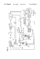
- FIG. 11 shows a system for evaluating an ADC in accordance with the invention, and it is to be noted that parts corresponding to those shown in FIGS. 3 and 4 are designated by like numerals as used before.
- the system comprises CPU 31 which performs data entry and delivery and calculations, a floating decimal point arithmetic chip 32 , a keyboard or a front panel 33 which is used to enter parameters or instructions, a display 34 which displays a menu selected by a user or results of determinations, and ROM 35 , RAM 36 or disk unit which store user inputs and data.
- the system comprises interleaver means 20 , and digital moving differentiator 22 ( 22 ′).
- a signal generator 11 which generates an analog signal is adapted to generate a sine wave, which is applied to an ADC 14 under test (or DUT).
- a timing controller 38 produces a clock, which is applied to the ADC 14 to control the timing of the A/D conversion within ADC 14 .
- a waveform memory (RAM Signal) 39 reads a digital signal which is stored in a buffer 41 connected to the output of the ADC 14 in synchronism with the end of conversion signal from the ADC 14 , for example.
- the waveform memory 39 may be written into in a sequential manner beginning with an address 0, and when a last address is written into, the write-in sequentially continues beginning from address 0 again.
- the waveform memory 39 may be of a size of 1024, for example (having a memory address of 0-1023).
- the analog signal generator 11 also generates a trigger signal, which starts a remaining sample counter 42 .
- a switch 43 which couples the buffer 41 to the waveform memory 39 is turned off, thus terminating the write-in of the digital signal into the waveform memory 39 .
- the write-in into the memory 39 is continually effected up to such point in time. Assuming that the last write-in address to the waveform memory 39 is 500 (1023), this last write-in address is read out from an address generator 44 and is incremented by one for remainder calculation, thus providing an address of 501 (0) where an oldest sample is stored. Thus, when the last write-in address to the waveform memory 39 is read out from the address generator 44 and incremented by one, individual samples can be read out in sequential order beginning with the oldest sample.
- the frequency f 0 and the amplitude A of the sine wave, the sampling frequency fs, the highest frequency f m of the pass band of a low pass filter 12 , and a number of remaining samples L which is predetermined as a trigger condition can be selected by a user and entered through the keyboard 33 or the front panel. These parameters may be previously written into a file saved in a disc and read from the file upon commencement of the test. CPU 31 writes these parameters into control registers associated with the signal generator 11 , the low pass filter 12 and the waveform memory 39 .
- FIG. 12 is a schematic view showing another arrangement of a system for evaluating an ADC according to the invention. Parts corresponding to those shown in FIG. 11 are designated by like numerals as used before. A difference over the arrangement of FIG. 11 resides in that wavelet transform means 46 ( 46 ′) is used in place of the digital moving differentiator 22 ( 22 ′) shown in FIG. 11 .
- FIG. 13 is a schematic view showing a further arrangement of a system for evaluating an ADC according to the invention, which differs from the arrangements shown in FIGS. 11 and 12 in that a control computer 48 exercises a control over the ADC evaluation system.
- the computer may comprise SPARC computer available from Sun Microsystems. This computer has the functions of CPU 31 , the floating decimal point calculator chip 32 , the keyboard 33 , the display 34 , ROM 35 , RAM 36 , the interleaver 20 , the digital moving differentiator 22 ( 22 ′) or wavelet transform means 46 ( 46 ′).
- FIG. 14A shows a schematic view of a system for evaluating an effective number of bits and differential non-linearity according to the invention, which functions to estimate an effective number of bits and DNL of an ADC 14 which internally contains a sample-and-hold circuit.
- a signal generator 11 which generates an analog signal provides a sine wave, which is applied to the ADC 14 under test.
- a timing controller 38 produces a clock which is applied to the ADC 14 for controlling the timing of the A/D conversion operation thereof.
- a waveform memory 39 accumulates a digital signal from the ADC 14 in synchronism with an end of conversion signal from the ADC 14 , for example.
- Instantaneous amplitude calculation means 21 forms suitable pairs of data ⁇ circumflex over (x) ⁇ [n] and ⁇ circumflex over (x) ⁇ [m] from an array of digital waveform read, determines a sum of squares in accordance with the equation (5), and also forms a square root of the sum of the square., to calculate an instantaneous amplitude
- the array of instantaneous amplitudes is applied as an input to interleaver means 20 , which then operates to form an interleaved signal from the amplitude A of the sine wave and the array of instantaneous amplitudes.
- the interleaved signal is supplied as an input to digital moving differentiator means 22 , which then operates to calculate a moving difference between a current input value and an immediately preceding input value. Since the input interleaved signal is arranged in the sequence of (A,
- the digital moving differentiator means 22 is designed to deliver one output every two samples, thus delivering the difference having an absolute amplitude of
- the instantaneous amplitude comprising M samples is input to the interleaver means 20 , the output of which is processed by the digital moving differentiator means 22 to provide a number of output samples which are equal to M.
- Maximum (or peak) detecting means 23 receives the array of difference signals as input, and operates to detect and deliver a maximum amplitude. A logarithm of the detected maximum amplitude is formed and is substituted into the equation (8.2) as a dB value, thereby allowing an instantaneous effective number of bits B to be estimated.
- the array of instantaneous amplitudes is also supplied to a digital moving differentiator means 22 ′, which sequentially delivers
- a maximum value among the outputs is detected by peak detecting means 237 and is substituted into the equation (7.2), allowing instantaneous DNL to be estimated.
- FIG. 14B shows an embodiment which estimates; an effective number of bits and DNL of an ADC which does not internally contains a sample-and-hold circuit.
- a sine wave from an analog signal generator 11 is retained in a sample-and-hold circuit 13 for a clock interval which is supplied from a clock generator 38 before it is applied to an ADC 14 under test.
- a waveform memory RAM 39 accumulates digital signals from the ADC 14 .
- the conversion operation by the ADC 14 is delayed by a delay element 51 responding to a clock so that the conversion takes place under a stabilized condition of the sample-hold-circuit 13 .
- the arrangement is similar to that shown in FIG. 14 A.
- a low pass filter 12 may be provided to eliminate distortion components from the sine wave generated by the signal generator 11 before it is applied to the ADC which internally houses a sample-and-hold circuit. Also in FIG. 14B, a similar low pass filter 12 may be provided on the output side of the signal generator 11 in FIG. 14B in order to eliminate distortion components.
- FIG. 15 shows an example of using wavelet transform means, using reference numerals as used before for parts which corresponds to those shown in FIG. 14 .
- an ADC 14 internally houses a sample-hold-circuit.
- Interleaved signal from interleaver means 20 is subject to the transform in the first stage 46 of the wavelet transform means, and a maximum value among the transforms or the dynamic range DR of the ADC is detected by the peak detecting means 23 .
- the value of the DR is substituted into the equation (8.2) to allow an instantaneous effective number of bits to be estimated.
- Transform outputs of the first stage 46 of the wavelet transform means or its components which are passed through the low pass filter is input to the second stage 46 ′ of the wavelet transform means where it is oversampled and is then subject to the high pass filtering in the second stage of the wavelet transform means.
- a maximum value among the results of such processing operation is detected by peak detecting means 23 ′ and is then substituted into the equation (9.1) to allow an instantaneous DNL to be estimated.
- a modification as shown in FIG. 14B may be applied for an ADC which does not internally house a sample-and-hold circuit.
- FIG. 6 shows an arrangement around the waveform memory in the system of the invention in detail.
- a sine wave from an analog signal generator 11 is applied to an ADC 14 under test, and a waveform memory 39 accumulates a digital signal from the ADC 14 .
- the analog signal generator 11 also generates a trigger signal, which starts a remaining sample counter 42 which is preset to a number of remaining samples L. Each time a new sample is received, the count in the counter 42 is decremented by one. When the count in the counter 42 becomes equal to zero, a switch 43 which is coupled to the waveform memory 39 is turned off to terminate the write-in of the digital signal to the wave form memory 39 .
- the CPU 38 shown in FIG. 11 or 12 , or the control computer 48 shown in FIG. 13 executes a command selected by a user or a commands from a file which is read from the disc, together with an associated sub-system.
- a command “hold an input signal” is given, the CPU or the control computer turns the switch 43 which is coupled to the waveform memory 39 off, thus terminating the write-in of the digital signal into the waveform memory 49 .
- a read-out of the digital waveform from the waveform memory 39 takes place as follows: It is initially assumed that the waveform memory 39 has a size of 1024, meaning that memory addresses are from 0 to 1023. If a last write-in address to the waveform memory 39 were 500 (of 1023), the last write-in address may be read out from the address generator 44 and incremented by one to provide an address of 501. An oldest sample is stored at this address. Thus, samples can be sequentially read out beginning with the oldest sample, by reading out the last write-in memory 39 from the address generator 44 and incrementing it by one.
- Means 53 for calculating “a number of offset samples between waveform memories which store digital waveforms having a phase difference of 90° therebetween”, which correspond to the cosine wave and the sine wave, is given the frequency f 0 of the sine wave and the sampling frequency fs of the ADC 14 to calculate “a number of offset samples k within the waveform memory 39 which stores the digital waveforms having a phase difference of 90° therebetween”.
- Instantaneous amplitude calculation means 21 takes digital waveforms for (M+k) samples from the waveform memory 39 where DA represents “a number of samples chosen for estimation for the effective number of bits” and k “a number of offset samples” which is determined by the number of offset samples calculation means 53 . The instantaneous amplitude calculation means 21 then forms pairs of ⁇ circumflex over (x) ⁇ [0] and ⁇ circumflex over (x) ⁇ [k], ⁇ circumflex over (x) ⁇ [1]and ⁇ circumflex over (x) ⁇ [k+1], . . .
- ⁇ circumflex over (x) ⁇ [M] and ⁇ circumflex over (x) ⁇ [M+k] in the array of digital waveforms which are taken by incrementing one for remainder calculation, and forms a sum of squares and then forms a square root of the sum of squares to calculate the instantaneous amplitude
- the array of instantaneous amplitudes is supplied to the interleaver means 20 as an input, which then produces an interleaved signal using the amplitude A of the sine wave and the array of instantaneous amplitudes.
- the interleaved signal produced by the interleaver means 20 is input to digital moving differentiator means 22 , which then calculates the moving differences from the interleaved signal.
- Peak detecting means 23 then receives the array of the difference signals and detects and delivers a maximum amplitude. A logarithm of the detected maximum amplitude is formed and is substituted to the equation (8.2), thus allowing the instantaneous effective number of bits B to be estimated Alternatively, the instantaneous amplitudes
- the maximum detecting means 23 receives the moving differences, compares the moving differences against the maximum value which is stored therein up to that point, stores and delivers a greater one of them as a maximum amplitude. When a logarithm of the detected maximum amplitude is formed, it may be substituted into the equation (8.2) to estimate the instantaneous effective number of bits B. Again, as, indicated in parentheses, the moving differentiator means 22 may be replaced by wavelet transform unit 46 . In this instance, M represents a number of wavelet transformed samples.
- the array of instantaneous amplitudes may be input to the digital moving differentiator means 22 ′, and the resulting moving differences may be input to the peak detecting means 23 ′, and a detected maximum value may be substituted into the equation (9.1) to estimate an instantaneous DNL.
- the interleaved signal may be input to the wavelet transform means 46 , and the output from the first stage thereof may be input to peak detecting means 23 , allowing an instantaneous effective number of bits B to be estimated from the detected peak value.
- the output from the first stage of the wavelet transform may be input to the second stage of the wavelet transform where it is oversampled to apply the second stage processing of the wavelet transform, and a peak of the transform outputs may be detected, thus allowing an instantaneous DNL to be estimated from this peak value.
- the processing operation takes place by using a computer as illustrated in FIGS. 11 to 13 , and accordingly, three peak detecting means shown in FIG. 16 share a common peak detecting function.
- a processing operation which occurs subsequent to the processing operation in the instantaneous amplitude calculation means 21 remains the same in subsequent embodiments and therefore will not be specifically described.
- FIG. 17 shows an arrangement around a waveform memory 39 in the system of the invention in detail. It is assumed that a real part waveform memory 39 R has a remaining sample counter 42 R associated therewith in which a number of remaining samples L is preset. Means for calculating “a number of offset samples in a digital waveform having a difference of 90° therebetween”, which correspond to the cosine wave and the sine wave, is supplied with the frequency f 0 of the sine wave and the sampling frequency fs of the ADC to calculate “a number of offset samples k in the digital waveform having a phase difference of 90° therebetween” according to the equation (10). An imaginary part waveform memory 39 I has a remaining sample counter 42 I associated therewith which is preset to L+k.
- a selection switch 43 associated with the waveform memory 39 now selects the real part waveform memory 39 R.
- a signal generator 11 which generates an analog signal generates a cosine wave, which is applied to an ADC 14 under test.
- the real part waveform memory 39 R accumulates a digital signal from the ADC 14 .
- a trigger signal generated by the analog signal generator 11 starts the remaining sample counters 42 R, 42 I, and when the count in the remaining sample counter 42 R becomes equal to zero, for example, a switch 43 R coupled to the real part waveform memory 39 R is turned off, terminating the write-in of the digital signal into the real part digital memory 39 R, followed by a selection of the imaginary part waveform memory 39 I by a selection switch 43 I associated therewith.
- the signal generator 11 which generates an analog signal generates a cosine wave, which is then applied to the ADC 14 under test.
- the imaginary part waveform memory 39 I accumulates a digital signal from the ADC 14 .
- a trigger signal generated by the analog signal generator 11 starts the remaining sample counter 42 I, and when the count in the remaining sample counter 42 I becomes equal to zero, for example, the switch 43 I coupled to the imaginary part waveform memory 39 I is turned off, terminating the write-in of the digital signal into the imaginary part waveform memory 39 I.
- Sine waves corresponding to the imaginary part are stored in the waveform memory 39 I for a number of offset samples k.
- Instantaneous amplitude calculation means 21 lakes digital waveforms for M samples from each of the real part waveform memory 39 R and the imaginary part waveform memory 39 I where M represents “a number of samples selected to estimate the effective number of bits”. Then, taking pairs of ⁇ circumflex over (x) ⁇ .re[0] and ⁇ circumflex over (x) ⁇ .im[0], ⁇ circumflex over (x) ⁇ .re[1] and ⁇ circumflex over (x) ⁇ .im[1], . . .
- the instantaneous amplitude calculation means 21 form a sum of squares and then calculates a square root of the sum of squares to determine an array of instantaneous amplitudes.
- ( x ⁇ . re ⁇ [ n ] 2 + x ⁇ . im ⁇ [ n ] 2 ) ( 11 )
- interleaver means 20 The array of instantaneous amplitudes is supplied to interleaver means 20 as an input.
- the arrangement and function remain the same as mentioned above in connection with FIG. 16, and therefor will not be specifically described.
- FIG. 18 shows a specific example of digital moving differentiator means 22 , which is non-cyclic filter represented by the following equation:
- y ( n ) h ( N ) x ( n ⁇ N )+ h ( N ⁇ 1) x ( n ⁇ N+ 1)+ . . . + h (1) x ( n ⁇ 1)+ h (0) x ( n ) (12.1)
- x(n) is supplied to a multiplier 61 and a one sample period delay element 62 and an output from the delay element 62 is supplied to a multiplier 63 .
- an output signal represents a difference between the current value x(n) and an immediately preceding value x(n ⁇ 1) of the input signal.
- the difference filter may be implemented in either a digital filter shown in FIG. 18 or a digital moving differentiator which is used to perform a calculation according to the equation (12.2).
- the “number of samples p per period” is used as a control input to a peak detector or finder.
- a processing operation takes place which comprises (a) forming a logarithm of the absolute magnitude of only local maxima and using it to deliver an instantaneous effective number of bits B according to the equation (8.2), and (b) delivering zeros for the remaining (p ⁇ 1) data.
- FIG. 19 shows a sequence of operations which take place within the wavelet transform unit 46 where Haar base function is used.
- a normalization factor of 1 ⁇ 2 is used here, but may be ⁇ fraction (1/ ⁇ square root ⁇ 2) ⁇ as is commonly used.
- k is changed to be n, n ⁇ 1, . . .
- FIGS. 20 and 21 show a flow of processing in the wavelet transform means when using base functions such as Daubechies.
- a scale corresponding to a period or “k” in 2 k ⁇ 1 is treated as “level k”.
- the algorithm of the wavelet transform is described in detail in “Wavelets and Subband Coding”, by Mathin Vetterli, Jelena Kovacevic, Prentice-Hall, 1995.
- the implementation of the wavelet transform in VLSI is; reported in “VSLI Implementation of Discrete Wavelet Transform”, by Aleksander Grezeszczak, Mrinal K. Mandal, Sethuraman Panchanathan, Tet Year), IEEE Trans. Very Large Scale Integration (VLSI) System, Vol. 4, No.
- the wavelet transform means may comprise the wavelet transform means shown in FIGS. 19, 20 and 21 or wavelet transform unit implemented VLSI.
- the oversampling Haar wavelet transform means may be implemented as follows: A low pass filter in the Haar-Wavelet transform has coefficients (1 ⁇ 2, 1 ⁇ 2), and a high pass filter has coefficients ( ⁇ 1 ⁇ 2, 1 ⁇ 2). Thus, the number of filter coefficients is equal to two. In this instance, a filtering takes place in dyadic translation of the base function along the time axis, as shown in FIG. 19 . For a(1), a(2); a(3), a(4); . . .
- a(N-1), a(N) ⁇ namely, ⁇ a(N), a(1), a(2), a(3), a(4), . . . , a(N-1) ⁇ so as to enable “a change in the signal between an even-numbered and an odd-numbered sample” to be detected by the wavelet transform.
- a procedure therefor will be described.
- the input signal ⁇ a(1), a(2), a(3), a(4), . . . , a(N ⁇ 1), a(N) ⁇ is subject to the Haar wavelet transform, then
- a cyclic shift version ⁇ a(N), a(1), a(2), a(3), a(4), a(N ⁇ 1) ⁇ is produced.
- FIGS. 22A and B graphically illustrate a comparison of the number of real number multiplications and the number of real number additions between the Daubechies-Wavelet transform and the FFT.
- a single Daubechies wavelet transform is substantially equivalent in its volume of computation to two Haar wavelet transforms.
- the number of real number multiplications is substantially equal for the Daubechies wavelet transform and the FFT.
- the number of real number multiplications for Daubechies-Wavelet transform becomes less than the number of real number multiplication for the FFT.
- the number of real number additions is less for the Daubechies wavelet transform than for the FFT.
- the “number of samples per period p i ” is used as a control input to the peak detector 23 . If the “p i >1”, a local maximum operation takes place.
- a processing operation takes place that (a) a logarithm of the absolute magnitude is formed only for local maxima, and an instantaneous effective number of bits B is estimated and delivered according to the equation (8.2), and (b) zeroes are delivered in place of the remaining (p i ⁇ 1) data. If “p i ⁇ 1”, zeroes are substituted for the input data to be delivered as outputs.
- FIG. 10B graphically illustrates a result of local maximum processing operation where 256 samples are taken from a sine wave over ten periods.
- an instantaneous effective number of bits and an instantaneous DNL can be estimated with a reduced volume of computation.
Abstract
Description


Claims (29)
Applications Claiming Priority (2)
| Application Number | Priority Date | Filing Date | Title |
|---|---|---|---|
| JP10-120324 | 1998-04-30 | ||
| JP12032498A JP3819589B2 (en) | 1998-04-30 | 1998-04-30 | AD converter evaluation device |
Publications (1)
| Publication Number | Publication Date |
|---|---|
| US6177894B1 true US6177894B1 (en) | 2001-01-23 |
Family
ID=14783443
Family Applications (1)
| Application Number | Title | Priority Date | Filing Date |
|---|---|---|---|
| US09/183,644 Expired - Lifetime US6177894B1 (en) | 1998-04-30 | 1998-10-30 | Evaluation system and method for AD converter |
Country Status (2)
| Country | Link |
|---|---|
| US (1) | US6177894B1 (en) |
| JP (1) | JP3819589B2 (en) |
Cited By (16)
| Publication number | Priority date | Publication date | Assignee | Title |
|---|---|---|---|---|
| US6281819B1 (en) * | 2000-04-03 | 2001-08-28 | Industrial Technology Research Institute | Device for ENOB estimation for ADC's based on dynamic deviation and method therefor |
| US6326909B1 (en) * | 1997-09-18 | 2001-12-04 | Advantest Corporation | Evaluation system for analog-digital or digital-analog converter |
| US20020136337A1 (en) * | 2001-03-20 | 2002-09-26 | Abhijit Chatterjee | Method and apparatus for high-resolution jitter measurement |
| US6476741B2 (en) * | 2000-04-19 | 2002-11-05 | Georgia Tech Research Corp. | Method and system for making optimal estimates of linearity metrics of analog-to-digital converters |
| US6557019B1 (en) * | 1999-09-07 | 2003-04-29 | Spectral Logic Design | Apparatus and method for compact Haar transform |
| US6658368B2 (en) * | 2001-03-23 | 2003-12-02 | International Business Machines Corporation | On-chip histogram testing |
| US20060001562A1 (en) * | 2004-06-30 | 2006-01-05 | Texas Instruments Incorporated | Method and system for sampling a signal |
| US7009538B1 (en) * | 2004-12-16 | 2006-03-07 | Tektronix, Inc. | High-speed DAC linearity measurement |
| DE102004047511A1 (en) * | 2004-09-28 | 2006-04-06 | Infineon Technologies Ag | Test device and method for testing analog-to-digital converters |
| US7146288B1 (en) * | 2002-07-18 | 2006-12-05 | Johnson Controls Technology Company | System and method for estimating quantization error in sampled data |
| US20090109072A1 (en) * | 2007-10-31 | 2009-04-30 | David Anderson | Testing of Analog to Digital Converters |
| US7619639B1 (en) * | 2005-09-12 | 2009-11-17 | Nvidia Corporation | Adaptive scaling using a programmable video engine |
| USRE41343E1 (en) * | 1999-11-19 | 2010-05-18 | Guido Wenning | Operational monitoring for a converter |
| US20140306689A1 (en) * | 2013-04-10 | 2014-10-16 | Texas Instruments, Incorporated | High resolution current pulse analog measurement |
| US9929739B1 (en) * | 2017-06-05 | 2018-03-27 | The Boeing Company | Methods and systems for determining integral non-linearity |
| US11796635B2 (en) | 2020-08-14 | 2023-10-24 | Nxp Usa, Inc. | Radar transceiver |
Families Citing this family (4)
| Publication number | Priority date | Publication date | Assignee | Title |
|---|---|---|---|---|
| JP2002168895A (en) * | 2000-11-30 | 2002-06-14 | Toyo Commun Equip Co Ltd | Aperture jitter measuring method and device |
| US20080247451A1 (en) * | 2007-03-13 | 2008-10-09 | Advantest Corporation | Measurement apparatus, measurement method, test apparatus, electronic device, and recording medium |
| US7778785B2 (en) * | 2008-02-14 | 2010-08-17 | Advantest Corporation | Signal-to-noise ratio measurement for discrete waveform |
| JP6095955B2 (en) * | 2012-11-16 | 2017-03-15 | ルネサスエレクトロニクス株式会社 | Measuring method, measuring apparatus and measuring program |
-
1998
- 1998-04-30 JP JP12032498A patent/JP3819589B2/en not_active Expired - Fee Related
- 1998-10-30 US US09/183,644 patent/US6177894B1/en not_active Expired - Lifetime
Non-Patent Citations (2)
| Title |
|---|
| Grezeszczak et al., VLSI implementation of discrete wavelet transform, IEEE Transactions, vol. 4, No. 4, 1996. * |
| Yamaguchi and Soma, "Dynamic Testing of ADCS Using Wavelet Transforms," Proceedings of IEEE International Test Conference, Nov. 1997, p. 379. |
Cited By (23)
| Publication number | Priority date | Publication date | Assignee | Title |
|---|---|---|---|---|
| US6326909B1 (en) * | 1997-09-18 | 2001-12-04 | Advantest Corporation | Evaluation system for analog-digital or digital-analog converter |
| US6476742B2 (en) * | 1997-09-18 | 2002-11-05 | Advantest Corporation | Evaluation system for analog-digital or digital-analog converter |
| US6557019B1 (en) * | 1999-09-07 | 2003-04-29 | Spectral Logic Design | Apparatus and method for compact Haar transform |
| USRE41343E1 (en) * | 1999-11-19 | 2010-05-18 | Guido Wenning | Operational monitoring for a converter |
| US6281819B1 (en) * | 2000-04-03 | 2001-08-28 | Industrial Technology Research Institute | Device for ENOB estimation for ADC's based on dynamic deviation and method therefor |
| US6476741B2 (en) * | 2000-04-19 | 2002-11-05 | Georgia Tech Research Corp. | Method and system for making optimal estimates of linearity metrics of analog-to-digital converters |
| US20020136337A1 (en) * | 2001-03-20 | 2002-09-26 | Abhijit Chatterjee | Method and apparatus for high-resolution jitter measurement |
| US6658368B2 (en) * | 2001-03-23 | 2003-12-02 | International Business Machines Corporation | On-chip histogram testing |
| US7146288B1 (en) * | 2002-07-18 | 2006-12-05 | Johnson Controls Technology Company | System and method for estimating quantization error in sampled data |
| US7109902B2 (en) * | 2004-06-30 | 2006-09-19 | Texas Instruments Incorporated | Method and system for sampling a signal |
| US20060001562A1 (en) * | 2004-06-30 | 2006-01-05 | Texas Instruments Incorporated | Method and system for sampling a signal |
| DE102004047511B4 (en) * | 2004-09-28 | 2006-07-13 | Infineon Technologies Ag | Test device and method for testing analog-to-digital converters |
| DE102004047511A1 (en) * | 2004-09-28 | 2006-04-06 | Infineon Technologies Ag | Test device and method for testing analog-to-digital converters |
| US20070216555A1 (en) * | 2004-09-28 | 2007-09-20 | Claus Dworski | Test Apparatus And Method For Testing Analog/Digital Converters |
| US7009538B1 (en) * | 2004-12-16 | 2006-03-07 | Tektronix, Inc. | High-speed DAC linearity measurement |
| TWI393904B (en) * | 2004-12-16 | 2013-04-21 | Tektronix Inc | High-speed dac linearity measurement |
| US7619639B1 (en) * | 2005-09-12 | 2009-11-17 | Nvidia Corporation | Adaptive scaling using a programmable video engine |
| US20090109072A1 (en) * | 2007-10-31 | 2009-04-30 | David Anderson | Testing of Analog to Digital Converters |
| US7561083B2 (en) * | 2007-10-31 | 2009-07-14 | Eagle Test Systems, Inc. | Testing of analog to digital converters |
| TWI469531B (en) * | 2007-10-31 | 2015-01-11 | Eagle Test Systems Inc | Testing of analog to digital converters |
| US20140306689A1 (en) * | 2013-04-10 | 2014-10-16 | Texas Instruments, Incorporated | High resolution current pulse analog measurement |
| US9929739B1 (en) * | 2017-06-05 | 2018-03-27 | The Boeing Company | Methods and systems for determining integral non-linearity |
| US11796635B2 (en) | 2020-08-14 | 2023-10-24 | Nxp Usa, Inc. | Radar transceiver |
Also Published As
| Publication number | Publication date |
|---|---|
| JPH11312975A (en) | 1999-11-09 |
| JP3819589B2 (en) | 2006-09-13 |
Similar Documents
| Publication | Publication Date | Title |
|---|---|---|
| US6326909B1 (en) | Evaluation system for analog-digital or digital-analog converter | |
| US6177894B1 (en) | Evaluation system and method for AD converter | |
| Peetz | Dynamic testing of waveform recorders | |
| US6549859B1 (en) | Method of time stamping a waveform edge of an input signal | |
| US7206722B2 (en) | Oscilloscope having an enhancement filter | |
| US4539518A (en) | Signal generator for digital spectrum analyzer | |
| US7538708B2 (en) | Efficient, selective error reduction for parallel, time-interleaved analog-to-digital converter | |
| JP2011228815A (en) | Frequency characteristic correction method for arbitrary waveform generator | |
| Petri | Frequency-domain testing of waveform digitizers | |
| Eduri et al. | Online calibration of a Nyquist-rate analog-to-digital converter using output code-density histograms | |
| DE102006005595A1 (en) | Transient noise emissions measuring method for use in e.g. electrical system, involves band-limiting digitalized noise signal by digital unit, computing continuous spectrogram by fourier transformation and evaluating by detector unit | |
| JP3257769B2 (en) | AD converter evaluation device | |
| Serra et al. | Fast ADC testing by repetitive histogram analysis | |
| JPH06506057A (en) | Method for determining the transmission characteristics of electrical conductors | |
| US6581016B1 (en) | Apparatus for accurately measuring impedance and method used therein | |
| US4995006A (en) | Apparatus and method for low-pass equivalent processing | |
| JP3257770B2 (en) | Evaluation device for DA converter | |
| Pálfi et al. | Efficient execution of ADC test with sine fitting with verification of excitation signal parameter settings | |
| US6281819B1 (en) | Device for ENOB estimation for ADC's based on dynamic deviation and method therefor | |
| JP3167472B2 (en) | Method for measuring SN ratio of analog-to-digital converter | |
| Mishra et al. | Determination of Nonlinearity and Effective Resolution of an A/D Converter for Arbitrary Application Input | |
| Jenq | Discrete-time method for signal-to-noise power ratio measurement | |
| Raze et al. | Non coherent spectral analysis of ADC using FFT windows: An alternative approach | |
| Deyst et al. | Bounds on frequency response estimates derived from uncertain step response data | |
| Carbone et al. | Sampling criteria for the estimation of multisine signal parameters |
Legal Events
| Date | Code | Title | Description |
|---|---|---|---|
| AS | Assignment |
Owner name: ADVANTEST CORPORATION, JAPAN Free format text: ASSIGNMENT OF ASSIGNORS INTEREST;ASSIGNOR:YAMAGUCI, TAKAHIRO;REEL/FRAME:009561/0401 Effective date: 19981021 |
|
| FEPP | Fee payment procedure |
Free format text: PAYOR NUMBER ASSIGNED (ORIGINAL EVENT CODE: ASPN); ENTITY STATUS OF PATENT OWNER: LARGE ENTITY Free format text: PAYER NUMBER DE-ASSIGNED (ORIGINAL EVENT CODE: RMPN); ENTITY STATUS OF PATENT OWNER: LARGE ENTITY |
|
| STCF | Information on status: patent grant |
Free format text: PATENTED CASE |
|
| FPAY | Fee payment |
Year of fee payment: 4 |
|
| FPAY | Fee payment |
Year of fee payment: 8 |
|
| FPAY | Fee payment |
Year of fee payment: 12 |
|
| AS | Assignment |
Owner name: ADVANTEST CORPORATION, JAPAN Free format text: CHANGE OF ADDRESS;ASSIGNOR:ADVANTEST CORPORATION;REEL/FRAME:047987/0626 Effective date: 20181112 |