US6165568A - Methods for forming field emission display devices - Google Patents
Methods for forming field emission display devices Download PDFInfo
- Publication number
- US6165568A US6165568A US09/023,661 US2366198A US6165568A US 6165568 A US6165568 A US 6165568A US 2366198 A US2366198 A US 2366198A US 6165568 A US6165568 A US 6165568A
- Authority
- US
- United States
- Prior art keywords
- surface region
- solution
- sodalime glass
- sulfuric acid
- glass surface
- Prior art date
- Legal status (The legal status is an assumption and is not a legal conclusion. Google has not performed a legal analysis and makes no representation as to the accuracy of the status listed.)
- Expired - Fee Related
Links
- 238000000034 method Methods 0.000 title claims abstract description 45
- 239000005361 soda-lime glass Substances 0.000 claims abstract description 76
- QAOWNCQODCNURD-UHFFFAOYSA-N Sulfuric acid Chemical compound OS(O)(=O)=O QAOWNCQODCNURD-UHFFFAOYSA-N 0.000 claims abstract description 62
- 229910052581 Si3N4 Inorganic materials 0.000 claims abstract description 59
- HQVNEWCFYHHQES-UHFFFAOYSA-N silicon nitride Chemical group N12[Si]34N5[Si]62N3[Si]51N64 HQVNEWCFYHHQES-UHFFFAOYSA-N 0.000 claims abstract description 59
- 239000003599 detergent Substances 0.000 claims abstract description 27
- VYPSYNLAJGMNEJ-UHFFFAOYSA-N Silicium dioxide Chemical compound O=[Si]=O VYPSYNLAJGMNEJ-UHFFFAOYSA-N 0.000 claims abstract description 24
- 239000000126 substance Substances 0.000 claims abstract description 17
- 239000000463 material Substances 0.000 claims abstract description 13
- 239000000377 silicon dioxide Substances 0.000 claims abstract description 12
- 229960001866 silicon dioxide Drugs 0.000 claims abstract description 12
- 235000012239 silicon dioxide Nutrition 0.000 claims abstract description 12
- MHAJPDPJQMAIIY-UHFFFAOYSA-N Hydrogen peroxide Chemical compound OO MHAJPDPJQMAIIY-UHFFFAOYSA-N 0.000 claims description 24
- QGZKDVFQNNGYKY-UHFFFAOYSA-N Ammonia Chemical compound N QGZKDVFQNNGYKY-UHFFFAOYSA-N 0.000 claims description 17
- 238000000151 deposition Methods 0.000 claims description 17
- 239000000758 substrate Substances 0.000 claims description 16
- BLRPTPMANUNPDV-UHFFFAOYSA-N Silane Chemical compound [SiH4] BLRPTPMANUNPDV-UHFFFAOYSA-N 0.000 claims description 13
- 239000002585 base Substances 0.000 claims description 12
- 229910021529 ammonia Inorganic materials 0.000 claims description 6
- 229910052760 oxygen Inorganic materials 0.000 claims description 5
- 238000013019 agitation Methods 0.000 claims description 4
- 229910052782 aluminium Inorganic materials 0.000 claims description 4
- 229910021645 metal ion Inorganic materials 0.000 claims description 4
- QVGXLLKOCUKJST-UHFFFAOYSA-N atomic oxygen Chemical compound [O] QVGXLLKOCUKJST-UHFFFAOYSA-N 0.000 claims description 3
- 229910052791 calcium Inorganic materials 0.000 claims description 3
- 229910052742 iron Inorganic materials 0.000 claims description 3
- 229910052749 magnesium Inorganic materials 0.000 claims description 3
- 239000001301 oxygen Substances 0.000 claims description 3
- 229910052700 potassium Inorganic materials 0.000 claims description 3
- 229910052708 sodium Inorganic materials 0.000 claims description 3
- 229910001413 alkali metal ion Inorganic materials 0.000 claims description 2
- 229910052718 tin Inorganic materials 0.000 claims description 2
- 230000001680 brushing effect Effects 0.000 claims 1
- 230000001590 oxidative effect Effects 0.000 abstract description 12
- 239000011521 glass Substances 0.000 abstract description 11
- 230000008021 deposition Effects 0.000 abstract description 8
- 239000007800 oxidant agent Substances 0.000 abstract description 3
- 238000004140 cleaning Methods 0.000 abstract description 2
- 230000008569 process Effects 0.000 description 8
- 241000252506 Characiformes Species 0.000 description 7
- 239000012535 impurity Substances 0.000 description 6
- 238000000623 plasma-assisted chemical vapour deposition Methods 0.000 description 6
- 238000007796 conventional method Methods 0.000 description 5
- 229910000069 nitrogen hydride Inorganic materials 0.000 description 5
- HUAUNKAZQWMVFY-UHFFFAOYSA-M sodium;oxocalcium;hydroxide Chemical compound [OH-].[Na+].[Ca]=O HUAUNKAZQWMVFY-UHFFFAOYSA-M 0.000 description 4
- 230000003746 surface roughness Effects 0.000 description 4
- XEEYBQQBJWHFJM-UHFFFAOYSA-N Iron Chemical compound [Fe] XEEYBQQBJWHFJM-UHFFFAOYSA-N 0.000 description 3
- 239000002253 acid Substances 0.000 description 3
- 238000012512 characterization method Methods 0.000 description 3
- 230000003247 decreasing effect Effects 0.000 description 3
- 239000008367 deionised water Substances 0.000 description 3
- 229910021641 deionized water Inorganic materials 0.000 description 3
- 238000010586 diagram Methods 0.000 description 3
- 239000012634 fragment Substances 0.000 description 3
- 239000000203 mixture Substances 0.000 description 3
- 229910000077 silane Inorganic materials 0.000 description 3
- XLYOFNOQVPJJNP-UHFFFAOYSA-N water Chemical compound O XLYOFNOQVPJJNP-UHFFFAOYSA-N 0.000 description 3
- QGZKDVFQNNGYKY-UHFFFAOYSA-O Ammonium Chemical compound [NH4+] QGZKDVFQNNGYKY-UHFFFAOYSA-O 0.000 description 2
- UFHFLCQGNIYNRP-UHFFFAOYSA-N Hydrogen Chemical compound [H][H] UFHFLCQGNIYNRP-UHFFFAOYSA-N 0.000 description 2
- UQSXHKLRYXJYBZ-UHFFFAOYSA-N Iron oxide Chemical compound [Fe]=O UQSXHKLRYXJYBZ-UHFFFAOYSA-N 0.000 description 2
- 238000004833 X-ray photoelectron spectroscopy Methods 0.000 description 2
- 230000002411 adverse Effects 0.000 description 2
- XAGFODPZIPBFFR-UHFFFAOYSA-N aluminium Chemical compound [Al] XAGFODPZIPBFFR-UHFFFAOYSA-N 0.000 description 2
- 238000004630 atomic force microscopy Methods 0.000 description 2
- 239000011575 calcium Substances 0.000 description 2
- 238000005336 cracking Methods 0.000 description 2
- 230000000694 effects Effects 0.000 description 2
- 238000005516 engineering process Methods 0.000 description 2
- 239000001257 hydrogen Substances 0.000 description 2
- 229910052739 hydrogen Inorganic materials 0.000 description 2
- 238000010348 incorporation Methods 0.000 description 2
- 239000011777 magnesium Substances 0.000 description 2
- 229910052751 metal Inorganic materials 0.000 description 2
- 239000002184 metal Substances 0.000 description 2
- 150000004767 nitrides Chemical class 0.000 description 2
- 238000012545 processing Methods 0.000 description 2
- 238000006748 scratching Methods 0.000 description 2
- 230000002393 scratching effect Effects 0.000 description 2
- 238000001004 secondary ion mass spectrometry Methods 0.000 description 2
- 239000011734 sodium Substances 0.000 description 2
- DDFHBQSCUXNBSA-UHFFFAOYSA-N 5-(5-carboxythiophen-2-yl)thiophene-2-carboxylic acid Chemical compound S1C(C(=O)O)=CC=C1C1=CC=C(C(O)=O)S1 DDFHBQSCUXNBSA-UHFFFAOYSA-N 0.000 description 1
- OYPRJOBELJOOCE-UHFFFAOYSA-N Calcium Chemical compound [Ca] OYPRJOBELJOOCE-UHFFFAOYSA-N 0.000 description 1
- OKTJSMMVPCPJKN-UHFFFAOYSA-N Carbon Chemical compound [C] OKTJSMMVPCPJKN-UHFFFAOYSA-N 0.000 description 1
- ZAMOUSCENKQFHK-UHFFFAOYSA-N Chlorine atom Chemical compound [Cl] ZAMOUSCENKQFHK-UHFFFAOYSA-N 0.000 description 1
- PXGOKWXKJXAPGV-UHFFFAOYSA-N Fluorine Chemical compound FF PXGOKWXKJXAPGV-UHFFFAOYSA-N 0.000 description 1
- DGAQECJNVWCQMB-PUAWFVPOSA-M Ilexoside XXIX Chemical compound C[C@@H]1CC[C@@]2(CC[C@@]3(C(=CC[C@H]4[C@]3(CC[C@@H]5[C@@]4(CC[C@@H](C5(C)C)OS(=O)(=O)[O-])C)C)[C@@H]2[C@]1(C)O)C)C(=O)O[C@H]6[C@@H]([C@H]([C@@H]([C@H](O6)CO)O)O)O.[Na+] DGAQECJNVWCQMB-PUAWFVPOSA-M 0.000 description 1
- FYYHWMGAXLPEAU-UHFFFAOYSA-N Magnesium Chemical compound [Mg] FYYHWMGAXLPEAU-UHFFFAOYSA-N 0.000 description 1
- OAICVXFJPJFONN-UHFFFAOYSA-N Phosphorus Chemical compound [P] OAICVXFJPJFONN-UHFFFAOYSA-N 0.000 description 1
- ZLMJMSJWJFRBEC-UHFFFAOYSA-N Potassium Chemical compound [K] ZLMJMSJWJFRBEC-UHFFFAOYSA-N 0.000 description 1
- 238000004458 analytical method Methods 0.000 description 1
- 230000008901 benefit Effects 0.000 description 1
- 230000015572 biosynthetic process Effects 0.000 description 1
- BRPQOXSCLDDYGP-UHFFFAOYSA-N calcium oxide Chemical compound [O-2].[Ca+2] BRPQOXSCLDDYGP-UHFFFAOYSA-N 0.000 description 1
- 239000000292 calcium oxide Substances 0.000 description 1
- ODINCKMPIJJUCX-UHFFFAOYSA-N calcium oxide Inorganic materials [Ca]=O ODINCKMPIJJUCX-UHFFFAOYSA-N 0.000 description 1
- 229910052799 carbon Inorganic materials 0.000 description 1
- 229910052801 chlorine Inorganic materials 0.000 description 1
- 239000000460 chlorine Substances 0.000 description 1
- 239000004020 conductor Substances 0.000 description 1
- 229910052731 fluorine Inorganic materials 0.000 description 1
- 239000011737 fluorine Substances 0.000 description 1
- 230000006872 improvement Effects 0.000 description 1
- 239000000395 magnesium oxide Substances 0.000 description 1
- CPLXHLVBOLITMK-UHFFFAOYSA-N magnesium oxide Inorganic materials [Mg]=O CPLXHLVBOLITMK-UHFFFAOYSA-N 0.000 description 1
- AXZKOIWUVFPNLO-UHFFFAOYSA-N magnesium;oxygen(2-) Chemical compound [O-2].[Mg+2] AXZKOIWUVFPNLO-UHFFFAOYSA-N 0.000 description 1
- 238000004519 manufacturing process Methods 0.000 description 1
- 239000011159 matrix material Substances 0.000 description 1
- 150000002739 metals Chemical class 0.000 description 1
- 238000012986 modification Methods 0.000 description 1
- 230000004048 modification Effects 0.000 description 1
- 239000011368 organic material Substances 0.000 description 1
- TWNQGVIAIRXVLR-UHFFFAOYSA-N oxo(oxoalumanyloxy)alumane Chemical compound O=[Al]O[Al]=O TWNQGVIAIRXVLR-UHFFFAOYSA-N 0.000 description 1
- 230000010287 polarization Effects 0.000 description 1
- 239000011591 potassium Substances 0.000 description 1
- CHWRSCGUEQEHOH-UHFFFAOYSA-N potassium oxide Chemical compound [O-2].[K+].[K+] CHWRSCGUEQEHOH-UHFFFAOYSA-N 0.000 description 1
- 229910001950 potassium oxide Inorganic materials 0.000 description 1
- 230000009467 reduction Effects 0.000 description 1
- KKCBUQHMOMHUOY-UHFFFAOYSA-N sodium oxide Chemical compound [O-2].[Na+].[Na+] KKCBUQHMOMHUOY-UHFFFAOYSA-N 0.000 description 1
- 229910001948 sodium oxide Inorganic materials 0.000 description 1
- 125000006850 spacer group Chemical group 0.000 description 1
- 239000011135 tin Substances 0.000 description 1
- 230000008016 vaporization Effects 0.000 description 1
- 238000009834 vaporization Methods 0.000 description 1
- 238000005406 washing Methods 0.000 description 1
Images


Classifications
-
- C—CHEMISTRY; METALLURGY
- C03—GLASS; MINERAL OR SLAG WOOL
- C03C—CHEMICAL COMPOSITION OF GLASSES, GLAZES OR VITREOUS ENAMELS; SURFACE TREATMENT OF GLASS; SURFACE TREATMENT OF FIBRES OR FILAMENTS MADE FROM GLASS, MINERALS OR SLAGS; JOINING GLASS TO GLASS OR OTHER MATERIALS
- C03C17/00—Surface treatment of glass, not in the form of fibres or filaments, by coating
- C03C17/22—Surface treatment of glass, not in the form of fibres or filaments, by coating with other inorganic material
- C03C17/225—Nitrides
-
- C—CHEMISTRY; METALLURGY
- C03—GLASS; MINERAL OR SLAG WOOL
- C03C—CHEMICAL COMPOSITION OF GLASSES, GLAZES OR VITREOUS ENAMELS; SURFACE TREATMENT OF GLASS; SURFACE TREATMENT OF FIBRES OR FILAMENTS MADE FROM GLASS, MINERALS OR SLAGS; JOINING GLASS TO GLASS OR OTHER MATERIALS
- C03C23/00—Other surface treatment of glass not in the form of fibres or filaments
- C03C23/008—Other surface treatment of glass not in the form of fibres or filaments comprising a lixiviation step
-
- C—CHEMISTRY; METALLURGY
- C23—COATING METALLIC MATERIAL; COATING MATERIAL WITH METALLIC MATERIAL; CHEMICAL SURFACE TREATMENT; DIFFUSION TREATMENT OF METALLIC MATERIAL; COATING BY VACUUM EVAPORATION, BY SPUTTERING, BY ION IMPLANTATION OR BY CHEMICAL VAPOUR DEPOSITION, IN GENERAL; INHIBITING CORROSION OF METALLIC MATERIAL OR INCRUSTATION IN GENERAL
- C23C—COATING METALLIC MATERIAL; COATING MATERIAL WITH METALLIC MATERIAL; SURFACE TREATMENT OF METALLIC MATERIAL BY DIFFUSION INTO THE SURFACE, BY CHEMICAL CONVERSION OR SUBSTITUTION; COATING BY VACUUM EVAPORATION, BY SPUTTERING, BY ION IMPLANTATION OR BY CHEMICAL VAPOUR DEPOSITION, IN GENERAL
- C23C16/00—Chemical coating by decomposition of gaseous compounds, without leaving reaction products of surface material in the coating, i.e. chemical vapour deposition [CVD] processes
- C23C16/02—Pretreatment of the material to be coated
- C23C16/0227—Pretreatment of the material to be coated by cleaning or etching
-
- C—CHEMISTRY; METALLURGY
- C23—COATING METALLIC MATERIAL; COATING MATERIAL WITH METALLIC MATERIAL; CHEMICAL SURFACE TREATMENT; DIFFUSION TREATMENT OF METALLIC MATERIAL; COATING BY VACUUM EVAPORATION, BY SPUTTERING, BY ION IMPLANTATION OR BY CHEMICAL VAPOUR DEPOSITION, IN GENERAL; INHIBITING CORROSION OF METALLIC MATERIAL OR INCRUSTATION IN GENERAL
- C23C—COATING METALLIC MATERIAL; COATING MATERIAL WITH METALLIC MATERIAL; SURFACE TREATMENT OF METALLIC MATERIAL BY DIFFUSION INTO THE SURFACE, BY CHEMICAL CONVERSION OR SUBSTITUTION; COATING BY VACUUM EVAPORATION, BY SPUTTERING, BY ION IMPLANTATION OR BY CHEMICAL VAPOUR DEPOSITION, IN GENERAL
- C23C16/00—Chemical coating by decomposition of gaseous compounds, without leaving reaction products of surface material in the coating, i.e. chemical vapour deposition [CVD] processes
- C23C16/22—Chemical coating by decomposition of gaseous compounds, without leaving reaction products of surface material in the coating, i.e. chemical vapour deposition [CVD] processes characterised by the deposition of inorganic material, other than metallic material
- C23C16/30—Deposition of compounds, mixtures or solid solutions, e.g. borides, carbides, nitrides
- C23C16/34—Nitrides
- C23C16/345—Silicon nitride
-
- H—ELECTRICITY
- H01—ELECTRIC ELEMENTS
- H01J—ELECTRIC DISCHARGE TUBES OR DISCHARGE LAMPS
- H01J9/00—Apparatus or processes specially adapted for the manufacture, installation, removal, maintenance of electric discharge tubes, discharge lamps, or parts thereof; Recovery of material from discharge tubes or lamps
- H01J9/24—Manufacture or joining of vessels, leading-in conductors or bases
- H01J9/241—Manufacture or joining of vessels, leading-in conductors or bases the vessel being for a flat panel display
-
- C—CHEMISTRY; METALLURGY
- C03—GLASS; MINERAL OR SLAG WOOL
- C03C—CHEMICAL COMPOSITION OF GLASSES, GLAZES OR VITREOUS ENAMELS; SURFACE TREATMENT OF GLASS; SURFACE TREATMENT OF FIBRES OR FILAMENTS MADE FROM GLASS, MINERALS OR SLAGS; JOINING GLASS TO GLASS OR OTHER MATERIALS
- C03C2217/00—Coatings on glass
- C03C2217/20—Materials for coating a single layer on glass
- C03C2217/28—Other inorganic materials
- C03C2217/281—Nitrides
-
- C—CHEMISTRY; METALLURGY
- C03—GLASS; MINERAL OR SLAG WOOL
- C03C—CHEMICAL COMPOSITION OF GLASSES, GLAZES OR VITREOUS ENAMELS; SURFACE TREATMENT OF GLASS; SURFACE TREATMENT OF FIBRES OR FILAMENTS MADE FROM GLASS, MINERALS OR SLAGS; JOINING GLASS TO GLASS OR OTHER MATERIALS
- C03C2218/00—Methods for coating glass
- C03C2218/10—Deposition methods
- C03C2218/15—Deposition methods from the vapour phase
- C03C2218/152—Deposition methods from the vapour phase by cvd
-
- C—CHEMISTRY; METALLURGY
- C03—GLASS; MINERAL OR SLAG WOOL
- C03C—CHEMICAL COMPOSITION OF GLASSES, GLAZES OR VITREOUS ENAMELS; SURFACE TREATMENT OF GLASS; SURFACE TREATMENT OF FIBRES OR FILAMENTS MADE FROM GLASS, MINERALS OR SLAGS; JOINING GLASS TO GLASS OR OTHER MATERIALS
- C03C2218/00—Methods for coating glass
- C03C2218/30—Aspects of methods for coating glass not covered above
- C03C2218/31—Pre-treatment
-
- H—ELECTRICITY
- H01—ELECTRIC ELEMENTS
- H01J—ELECTRIC DISCHARGE TUBES OR DISCHARGE LAMPS
- H01J2201/00—Electrodes common to discharge tubes
- H01J2201/30—Cold cathodes
- H01J2201/304—Field emission cathodes
-
- H—ELECTRICITY
- H01—ELECTRIC ELEMENTS
- H01J—ELECTRIC DISCHARGE TUBES OR DISCHARGE LAMPS
- H01J2329/00—Electron emission display panels, e.g. field emission display panels
Definitions
- the invention encompasses methods of depositing silicon nitride on sodalime glass surfaces and to methods of forming field emission display devices.
- Flat-panel displays are widely used to visually display information where the physical thickness and bulk of a conventional cathode ray tube is unacceptable or impractical.
- Portable electronic devices and systems have benefitted from the use of flat-panel displays, which require less space and result in a lighter, more compact display system than provided by conventional cathode ray tube technology.
- a particular type of flat-panel display is the field emission flat-panel display.
- a field emission flat-panel display an electron emitting cathode plate is separated from a display face or faceplate at a relatively small, uniform distance. The intervening space between these elements is evacuated.
- Field emission displays have the outward appearance of a CRT except that they are very thin. While being simple, they are also capable of very high resolutions. In some cases, they can be assembled by use of technology already used in integrated circuit production.
- Field emission flat-panel displays utilize field emission devices, in groups or individually, to emit electrons that energize a cathodoluminescent material deposited on a surface of a viewing screen or display faceplate.
- the emitted electrons originate from an emitter or cathode electrode at a region of geometric discontinuity having a sharp edge or tip.
- Electron emission is induced by application of potentials of appropriate polarization and magnitude to the various electrodes of the field emission display device, which are typically arranged in a two-dimensional matrix array.
- a field emission display device 10 is illustrated schematically in FIG. 1.
- Device 10 comprises a faceplate 12 comprising a transparent conductor. Underlying faceplate 12 are phosphor dots 14.
- a spacer 16 is provided to space faceplate 12 from a series of column electrodes 18 and emitters 20. Column electrodes 18 and emitters 20 overlay row electrodes 22, which in turn overlay a baseplate 24.
- Baseplate 24 is typically made out of sodalime glass, and typically comprises a layer of silicon nitride formed between baseplate 24 and emitters 20.
- the silicon nitride is deposited to provide a buffer layer between glass and subsequent layers. This results in better stress control and adhesion between the subsequent metal, emitter and grid layers. Another advantage of this buffer layer is that it can cap or prevent impurities within the glass from entering into other parts of the device structure. Emitters 20 are thus at least partially supported by the layer of silicon nitride.
- the silicon nitride can be deposited by a number of conventional methods, including, for example, a plasma enhanced chemical vapor deposition process utilizing silane and ammonium gasses.
- An example deposition method comprises placing a glass substrate within a reactor.
- the pressure within the reactor is maintained at about 1000 mTorr, and a power within the reactor is maintained at about 500 watts.
- a mixture of SiH 4 and NH 3 is flowed into the reactor.
- a flow rate of the SiH 4 is 100 standard cubic centimeters (sccm).
- a flow rate of the NH 3 is 450 sccm.
- the deposited silicon nitride disadvantageously has a tensile stress which renders the silicon nitride prone to scratching and cracking.
- the invention encompasses methods of treating sodalime glass surfaces for deposition of silicon nitride and methods of forming field emission display devices.
- the invention encompasses a method of treating a sodalime glass surface for deposition of silicon nitride.
- a surface of the glass is cleaned with a detergent and contacted with a solution comprising a strong oxidant to remove non-silicon-dioxide materials from the surface and from a zone underlying and proximate the surface.
- the invention encompasses a method of depositing silicon nitride.
- a surface of a sodalime glass substrate is contacted with a solution comprising sulfuric acid and hydrogen peroxide to remove non-silicon-dioxide materials from the surface and from a zone underlying and proximate the surface.
- the surface is then exposed to a mixture of SiH 4 , NH 3 and H 2 to deposit silicon nitride on the surface.
- the invention encompasses a method of depositing silicon nitride on a sodalime glass surface.
- a sodalime glass surface is provided and contacted with a detergent solution.
- the detergent solution is agitated across the sodalime glass surface and then removed from the sodalime glass surface by rinsing it in deionized water at about 80° C.
- the sodalime glass surface is contacted with a sulfuric acid solution to remove non-silicon-dioxide materials from the surface and from a zone underlying and proximate the surface.
- the sulfuric acid solution is then removed from the sodalime glass surface.
- nitride is deposited on the sodalime glass surface.
- the invention encompasses a method of forming field emission display device.
- a base plate is formed.
- the forming of the base plate comprises the following steps.
- a base plate substrate is provided.
- the base plate substrate comprises a sodalime glass surface having a first concentration of an undesired chemical.
- the sodalime glass surface is contacted with a detergent solution.
- the detergent solution is agitated across the sodalime glass surface and then removed.
- the sodalime glass surface is contacted with a sulfuric acid solution to extract at least some of the undesired chemical from the sodalime glass surface and from a zone underlying and proximate the surface.
- the sulfuric acid solution and the extracted undesired chemical are removed from the sodalime glass surface.
- the sodalime glass surface comprises less than the first concentration of the undesired chemical.
- FIG. 1 is a schematic cross-sectional view of a prior art field emission display device.
- FIG. 2 is a block diagram of a process of the present invention.
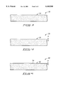
- FIG. 3 is a schematic cross-sectional view of a sodalime glass fragment being treated according to a method of the present invention.
- FIG. 4 is a schematic cross-sectional view of the FIG. 3 sodalime glass fragment at a processing step subsequent to that of FIG. 3.
- FIG. 5 is a schematic cross-sectional view of the FIG. 3 sodalime glass fragment at a processing step subsequent to that of FIG. 4.
- a method of forming denser silicon nitride is to deposit silicon nitride with a plasma enhanced chemical vapor deposition process utilizing silane, hydrogen and ammonium gasses.
- An example deposition method comprises placing a glass substrate within a reactor.
- the pressure within the reactor is maintained at about 1000 mTorr, and a power within the reactor is maintained at about 500 watts.
- a mixture of SiH 4 , H 2 and NH 3 is flowed into the reactor.
- a flow rate of the SiH 4 is about 100 standard cubic centimeters (sccm).
- a flow rated of the H 2 is from about 650 sccm to about 750 sccm, and preferably about 730 sccm.
- a flow rate of the NH 3 is about 450 sccm.
- Silicon nitride deposited by the above example process of the present invention is denser than silicon nitride deposited by a conventional process as evidenced by a decreased etch rate of the silicon nitride deposited by the example process of the present invention.
- An etch rate of silicon nitride deposited by the example process of the present invention is 750 angstroms/minute with a buffered oxide etchant comprising ammonium fluoride and HF.
- An etch rate of silicon nitride deposited by a conventional method is 2200 angstroms/minute under identical conditions.
- the present invention encompasses a treatment method which removes non-silicon-dioxide materials from proximate a sodalime glass surface prior to formation of a silicon nitride layer on the surface.
- the present invention encompasses providing a sodalime glass substrate.
- the sodalime glass substrate may be configured, for example, for incorporation as a baseplate in a field emission display device.
- Sodalime glass generally comprises about 75 weight percent of silicon dioxide and about 25 weight percent of a combination of one or more of sodium oxide, potassium oxide, magnesium oxide, aluminum oxide, iron oxide and calcium oxide.
- the non-silicon-dioxide materials of sodalime glass can adversely affect deposition of silicon nitride.
- the present invention encompasses a pretreatment step which can reduce the amount of non-silicon-dioxide materials at a surface of a sodalime glass prior to deposition of silicon nitride.
- a pretreatment of the present invention comprises the two steps indicated as steps B and C.
- Step B comprises washing a surface of the sodalime glass with a detergent solution.
- a suitable detergent has been found to be DNS,TM TS-400G,TM manufactured by Dianippon Screen, Japan.
- the detergent solution may be vigorously applied to the sodalime glass surface by either mechanical agitation or by ultrasonically vibrating the detergent solution across the glass surface. Methods for agitation of a detergent solution against a glass surface and for ultrasonically vibrating a detergent solution across a glass surface are known to persons of ordinary skill in the art.
- the detergent can be removed from the sodalime glass surface (in a step which is not shown in FIG. 2) by conventional methods, such as by a deionized water wash and an air dry.
- the washed surface of the sodalime glass is subjected to a piranha clean.
- piranha clean will comprise exposing the sodalime glass surface to a solution comprising sulfuric acid and hydrogen peroxide.
- a preferred concentration of the sulfuric acid and hydrogen peroxide within the piranha clean is 100 parts of sulfuric acid per part of hydrogen peroxide (by volume).
- sulfuric acid and hydrogen peroxide are generally known to be strong oxidants.
- the piranha clean is a strongly oxidizing solution.
- Such strongly oxidizing solution can, for example, oxidize organic materials to assist in removing the materials from the sodalime glass surface.
- an effect of the piranha clean is understood to be the removal of alkaline metals, aluminum and iron from the surface of a sodalime glass.
- the present invention encompasses exposing a sodalime surface to a strong acid.
- the temperature of at least one of the exposed sodalime glass surface, and of the oxidizing solution is controlled during exposure of the sodalime glass surface to the oxidizing solution.
- the is controlled temperature will preferably be from about 20° C. to about 100° C., and will most preferably be about 85° C. It has been found experimentally that at temperatures of 85° C. effective results can be achieved after only 15 minutes of treatment of the sodalime glass surface with the oxidizing solution. It has also been found that temperatures above 100° C. are typically not desired due to vaporization of the acid in the oxidizing solution.
- the pressure during exposure of a sodalime glass surface to the oxidizing solution is preferably about one atmosphere.
- the temperature will preferably be controlled during the majority of a period of time that the sodalime glass surface is exposed to the oxidizing solution. It is recognized that unless the sodalime surface and the oxidizing solution are preheated, there would likely be a short period of time during initial exposure of the oxidizing solution and the sodalime glass surface when one or both are not at the desired controlled temperature. This lack of desired temperature during initial exposure is not expected to significantly adversely affect methods of the present invention.
- the solution can be removed from the surface (in a step which is not shown in FIG. 2) by conventional methods, such as by a deionized water wash and an air dry.
- a silicon nitride layer is deposited on the treated surface of the sodalime glass.
- the silicon nitride layer can be deposited by conventional methods, or by plasma enhanced chemical vapor deposition utilizing silane, ammonia and hydrogen gasses.
- a sodalime glass substrate 50 is illustrated.
- Substrate 50 comprises a surface 52 and a number of impurities (shown as stippling) beneath surface 52.
- the impurities comprise the non-silicon-dioxide components of sodalime glass substrate 50.
- Such impurities can comprise, for example, oxygen, metal ions, alkali metal ions, and alkaline metal ions.
- the non-silicon-dioxide materials of a sodalime glass typically comprise one or more elements selected from the group consisting of Na, K, O, Ca, Mg, Sn, Fe, and Al. In accordance with the present invention, it is recognized that such elements may constitute undesired chemicals at a sodalime surface in the context of attempting to deposit silicon nitride on such surface.
- the sodalime fragment of FIG. 3 is shown after being subjected to a pretreatment step of the present invention.
- a pretreatment step comprises exposure of surface 52 to a piranha clean, and preferably also comprises exposure of surface 52 to a detergent-based clean in advance thereof.
- the pretreatment steps of the present invention advantageously remove impurities from surface 52 and from a zone "X" underlying and proximate surface 52. Zone "X" and surface 52 together comprise a surface region.
- a silicon nitride layer 54 is deposited over IN surface 52.
- depositing silicon nitride layer 54 over surface 52 after the above-discussed pretreatment steps can advantageously improve clarity of the silicon nitride layer. It is also recognized that depositing silicon nitride layer 54 over surface 52 after the above-discussed pretreatment steps can advantageously decrease surface imperfections within the silicon nitride layer relative to deposition of a silicon nitride layer without utilizing such pretreatment steps.
- sodalime glass substrate 50 can be incorporated, for example, into a field emission display device (such as that shown in FIG. 1) as a baseplate.
- Such reduction of contaminating materials within a silicon nitride layer is found to improve the clarity of the layer and to also improve surface characteristics of the layer. Such improvement in clarity and surface characteristics improves a suitability of the silicon nitride layers for utilization in field emission display devices.
- the silicon nitride layer formed after a pretreatment step of the present invention thus has a decreased surface roughness relative to a silicon nitride layer formed without such pretreatment. Such decreased surface roughness improves a suitability of the silicon nitride layer formed after the pretreatment for utilization in field emission display devices relative to the silicon nitride layer formed without the pretreatment.
Landscapes
- Chemical & Material Sciences (AREA)
- Engineering & Computer Science (AREA)
- Materials Engineering (AREA)
- Chemical Kinetics & Catalysis (AREA)
- General Chemical & Material Sciences (AREA)
- Organic Chemistry (AREA)
- Geochemistry & Mineralogy (AREA)
- Life Sciences & Earth Sciences (AREA)
- Mechanical Engineering (AREA)
- Metallurgy (AREA)
- Manufacturing & Machinery (AREA)
- Inorganic Chemistry (AREA)
- Surface Treatment Of Glass (AREA)
Abstract
Description
Claims (18)
Priority Applications (2)
| Application Number | Priority Date | Filing Date | Title |
|---|---|---|---|
| US09/023,661 US6165568A (en) | 1998-02-09 | 1998-02-09 | Methods for forming field emission display devices |
| US09/707,441 US6440505B1 (en) | 1998-02-09 | 2000-11-06 | Methods for forming field emission display devices |
Applications Claiming Priority (1)
| Application Number | Priority Date | Filing Date | Title |
|---|---|---|---|
| US09/023,661 US6165568A (en) | 1998-02-09 | 1998-02-09 | Methods for forming field emission display devices |
Related Child Applications (1)
| Application Number | Title | Priority Date | Filing Date |
|---|---|---|---|
| US09/707,441 Continuation US6440505B1 (en) | 1998-02-09 | 2000-11-06 | Methods for forming field emission display devices |
Publications (1)
| Publication Number | Publication Date |
|---|---|
| US6165568A true US6165568A (en) | 2000-12-26 |
Family
ID=21816485
Family Applications (2)
| Application Number | Title | Priority Date | Filing Date |
|---|---|---|---|
| US09/023,661 Expired - Fee Related US6165568A (en) | 1998-02-09 | 1998-02-09 | Methods for forming field emission display devices |
| US09/707,441 Expired - Fee Related US6440505B1 (en) | 1998-02-09 | 2000-11-06 | Methods for forming field emission display devices |
Family Applications After (1)
| Application Number | Title | Priority Date | Filing Date |
|---|---|---|---|
| US09/707,441 Expired - Fee Related US6440505B1 (en) | 1998-02-09 | 2000-11-06 | Methods for forming field emission display devices |
Country Status (1)
| Country | Link |
|---|---|
| US (2) | US6165568A (en) |
Cited By (2)
| Publication number | Priority date | Publication date | Assignee | Title |
|---|---|---|---|---|
| US6440505B1 (en) * | 1998-02-09 | 2002-08-27 | Micron Technology, Inc. | Methods for forming field emission display devices |
| WO2003007368A3 (en) * | 2001-07-12 | 2003-03-27 | Advanced Micro Devices Inc | Method of forming nitride capped cu lines with reduced electromigration along the cu/nitride interface |
Families Citing this family (1)
| Publication number | Priority date | Publication date | Assignee | Title |
|---|---|---|---|---|
| US7415841B2 (en) * | 2002-03-27 | 2008-08-26 | Hoya Corporation | Method for producing chemically strengthened glass substrate for information recording medium |
Citations (9)
| Publication number | Priority date | Publication date | Assignee | Title |
|---|---|---|---|---|
| US3549411A (en) * | 1967-06-27 | 1970-12-22 | Texas Instruments Inc | Method of preparing silicon nitride films |
| US3753840A (en) * | 1970-01-19 | 1973-08-21 | Glaverbel | Fabrication of curved glass sheets |
| US4664934A (en) * | 1985-02-07 | 1987-05-12 | Toyoda Gosei Co., Ltd. | Process for manufacturing solid electrochromic element |
| US4975760A (en) * | 1986-03-06 | 1990-12-04 | Kabushiki Kaisha Toshiba | Electrode interconnection material, semiconductor device using this material and driving circuit substrate for display device |
| US5034795A (en) * | 1988-11-10 | 1991-07-23 | Thomson Tubes Electroniques | Electrically insulating substrate |
| US5189551A (en) * | 1989-07-27 | 1993-02-23 | Monsanto Company | Solar screening film for a vehicle windshield |
| US5585301A (en) * | 1995-07-14 | 1996-12-17 | Micron Display Technology, Inc. | Method for forming high resistance resistors for limiting cathode current in field emission displays |
| US5725957A (en) * | 1994-07-29 | 1998-03-10 | Donnelly Corporation | Transparent substrate with diffuser surface |
| US5846628A (en) * | 1992-09-02 | 1998-12-08 | Mitsubishi Kasei Corporation | Magnetic disc |
Family Cites Families (2)
| Publication number | Priority date | Publication date | Assignee | Title |
|---|---|---|---|---|
| AU736751B2 (en) * | 1996-12-26 | 2001-08-02 | Canon Kabushiki Kaisha | Electron source substrate and electron source and image-forming apparatus using such substrate as well as method of manufacturing the same |
| US6165568A (en) * | 1998-02-09 | 2000-12-26 | Micron Technology, Inc. | Methods for forming field emission display devices |
-
1998
- 1998-02-09 US US09/023,661 patent/US6165568A/en not_active Expired - Fee Related
-
2000
- 2000-11-06 US US09/707,441 patent/US6440505B1/en not_active Expired - Fee Related
Patent Citations (9)
| Publication number | Priority date | Publication date | Assignee | Title |
|---|---|---|---|---|
| US3549411A (en) * | 1967-06-27 | 1970-12-22 | Texas Instruments Inc | Method of preparing silicon nitride films |
| US3753840A (en) * | 1970-01-19 | 1973-08-21 | Glaverbel | Fabrication of curved glass sheets |
| US4664934A (en) * | 1985-02-07 | 1987-05-12 | Toyoda Gosei Co., Ltd. | Process for manufacturing solid electrochromic element |
| US4975760A (en) * | 1986-03-06 | 1990-12-04 | Kabushiki Kaisha Toshiba | Electrode interconnection material, semiconductor device using this material and driving circuit substrate for display device |
| US5034795A (en) * | 1988-11-10 | 1991-07-23 | Thomson Tubes Electroniques | Electrically insulating substrate |
| US5189551A (en) * | 1989-07-27 | 1993-02-23 | Monsanto Company | Solar screening film for a vehicle windshield |
| US5846628A (en) * | 1992-09-02 | 1998-12-08 | Mitsubishi Kasei Corporation | Magnetic disc |
| US5725957A (en) * | 1994-07-29 | 1998-03-10 | Donnelly Corporation | Transparent substrate with diffuser surface |
| US5585301A (en) * | 1995-07-14 | 1996-12-17 | Micron Display Technology, Inc. | Method for forming high resistance resistors for limiting cathode current in field emission displays |
Non-Patent Citations (6)
| Title |
|---|
| Abstract: Kato, Y., et al., "Effect of Washing Methods on AMLCD Glass Substrates Treated With BHF", pp. 33-34. (No Date Available). |
| Abstract: Kato, Y., et al., Effect of Washing Methods on AMLCD Glass Substrates Treated With BHF , pp. 33 34. (No Date Available). * |
| Abstract: Walter, A.E., et al., "Effective Particle Removal Using an Enclosed Process Chamber for FPD Chemical Cleaning", pp. 37-39. (No Date Available). |
| Abstract: Walter, A.E., et al., Effective Particle Removal Using an Enclosed Process Chamber for FPD Chemical Cleaning , pp. 37 39. (No Date Available). * |
| Textbook excerpt: Chapter Two: Display Manufacturing, "Liquid Crystal Flat Panel Displays", (1993), pp. 63-66, Van Hostrand Reinhold. (No Month Available). |
| Textbook excerpt: Chapter Two: Display Manufacturing, Liquid Crystal Flat Panel Displays , (1993), pp. 63 66, Van Hostrand Reinhold. (No Month Available). * |
Cited By (2)
| Publication number | Priority date | Publication date | Assignee | Title |
|---|---|---|---|---|
| US6440505B1 (en) * | 1998-02-09 | 2002-08-27 | Micron Technology, Inc. | Methods for forming field emission display devices |
| WO2003007368A3 (en) * | 2001-07-12 | 2003-03-27 | Advanced Micro Devices Inc | Method of forming nitride capped cu lines with reduced electromigration along the cu/nitride interface |
Also Published As
| Publication number | Publication date |
|---|---|
| US6440505B1 (en) | 2002-08-27 |
Similar Documents
| Publication | Publication Date | Title |
|---|---|---|
| US6545407B1 (en) | Electron emission apparatus | |
| US8168481B2 (en) | Method of manufacturing SOI substrate | |
| KR100391840B1 (en) | Method and apparatus for forming an insulating film on the surface of a semiconductor substrate | |
| US7442623B2 (en) | Method for manufacturing bonded substrate and bonded substrate manufactured by the method | |
| KR100531337B1 (en) | Plasma treatment method and manufacturing method of semiconductor device | |
| EP1021818B1 (en) | Cleaning of electron-emissive elements | |
| JPH1187341A (en) | Film forming method and film forming apparatus | |
| JP2003023000A5 (en) | ||
| US6165568A (en) | Methods for forming field emission display devices | |
| CN1910059A (en) | Methods for cleaning a set of structures comprising yttrium oxide in a plasma processing system | |
| KR20010050758A (en) | Plasma CVD system and plasma CVD film deposition method | |
| JPH1140502A (en) | Dry cleaning method for semiconductor manufacturing equipment | |
| JP5642427B2 (en) | Plasma processing method | |
| US6329294B1 (en) | Method for removing photoresist mask used for etching of metal layer and other etching by-products | |
| JP2646811B2 (en) | Dry etching method | |
| Somashekhar et al. | Hydrogen Plasma Removal of Post‐RIE Residue for Backend Processing | |
| CN117912940A (en) | A high temperature oxidation process method for silicon carbide device | |
| US6410101B1 (en) | Method for scrubbing and passivating a surface of a field emission display | |
| US6235545B1 (en) | Methods of treating regions of substantially upright silicon-comprising structures, method of treating silicon-comprising emitter structures, methods of forming field emission display devices, and cathode assemblies | |
| US7101586B2 (en) | Method to increase the emission current in FED displays through the surface modification of the emitters | |
| JPH0661198A (en) | Method of manufacturing thin film element | |
| JPH08255555A (en) | Needle electrode and manufacturing method thereof | |
| JPS6350854B2 (en) | ||
| JP2822460B2 (en) | Multi-layer wiring formation method | |
| Snitovskii et al. | The Effect of Contact Window Cleaning and Doping in BF3+ H2and BF3+ H2+ CF4Plasmas on the Mo–p+-Si Contact Resistance |
Legal Events
| Date | Code | Title | Description |
|---|---|---|---|
| AS | Assignment |
Owner name: MICRON TECHNOLOGY, INC., IDAHO Free format text: ASSIGNMENT OF ASSIGNORS INTEREST;ASSIGNOR:RAINA, KANWAL;REEL/FRAME:009099/0207 Effective date: 19980204 |
|
| FEPP | Fee payment procedure |
Free format text: PAYOR NUMBER ASSIGNED (ORIGINAL EVENT CODE: ASPN); ENTITY STATUS OF PATENT OWNER: LARGE ENTITY |
|
| CC | Certificate of correction | ||
| FPAY | Fee payment |
Year of fee payment: 4 |
|
| FPAY | Fee payment |
Year of fee payment: 8 |
|
| REMI | Maintenance fee reminder mailed | ||
| LAPS | Lapse for failure to pay maintenance fees | ||
| STCH | Information on status: patent discontinuation |
Free format text: PATENT EXPIRED DUE TO NONPAYMENT OF MAINTENANCE FEES UNDER 37 CFR 1.362 |
|
| FP | Lapsed due to failure to pay maintenance fee |
Effective date: 20121226 |