US6151656A - Memory apparatus and method for controlling memory access based on memory address directivity - Google Patents
Memory apparatus and method for controlling memory access based on memory address directivity Download PDFInfo
- Publication number
- US6151656A US6151656A US09/031,543 US3154398A US6151656A US 6151656 A US6151656 A US 6151656A US 3154398 A US3154398 A US 3154398A US 6151656 A US6151656 A US 6151656A
- Authority
- US
- United States
- Prior art keywords
- memory
- address
- memories
- highspeed
- access control
- Prior art date
- Legal status (The legal status is an assumption and is not a legal conclusion. Google has not performed a legal analysis and makes no representation as to the accuracy of the status listed.)
- Expired - Fee Related
Links
Images

Classifications
-
- G—PHYSICS
- G09—EDUCATION; CRYPTOGRAPHY; DISPLAY; ADVERTISING; SEALS
- G09G—ARRANGEMENTS OR CIRCUITS FOR CONTROL OF INDICATING DEVICES USING STATIC MEANS TO PRESENT VARIABLE INFORMATION
- G09G5/00—Control arrangements or circuits for visual indicators common to cathode-ray tube indicators and other visual indicators
- G09G5/36—Control arrangements or circuits for visual indicators common to cathode-ray tube indicators and other visual indicators characterised by the display of a graphic pattern, e.g. using an all-points-addressable [APA] memory
- G09G5/39—Control of the bit-mapped memory
-
- G—PHYSICS
- G06—COMPUTING; CALCULATING OR COUNTING
- G06F—ELECTRIC DIGITAL DATA PROCESSING
- G06F12/00—Accessing, addressing or allocating within memory systems or architectures
- G06F12/02—Addressing or allocation; Relocation
- G06F12/0207—Addressing or allocation; Relocation with multidimensional access, e.g. row/column, matrix
-
- G—PHYSICS
- G06—COMPUTING; CALCULATING OR COUNTING
- G06K—GRAPHICAL DATA READING; PRESENTATION OF DATA; RECORD CARRIERS; HANDLING RECORD CARRIERS
- G06K15/00—Arrangements for producing a permanent visual presentation of the output data, e.g. computer output printers
- G06K15/02—Arrangements for producing a permanent visual presentation of the output data, e.g. computer output printers using printers
- G06K15/10—Arrangements for producing a permanent visual presentation of the output data, e.g. computer output printers using printers by matrix printers
-
- G—PHYSICS
- G06—COMPUTING; CALCULATING OR COUNTING
- G06K—GRAPHICAL DATA READING; PRESENTATION OF DATA; RECORD CARRIERS; HANDLING RECORD CARRIERS
- G06K2215/00—Arrangements for producing a permanent visual presentation of the output data
- G06K2215/0002—Handling the output data
- G06K2215/0062—Handling the output data combining generic and host data, e.g. filling a raster
-
- G—PHYSICS
- G09—EDUCATION; CRYPTOGRAPHY; DISPLAY; ADVERTISING; SEALS
- G09G—ARRANGEMENTS OR CIRCUITS FOR CONTROL OF INDICATING DEVICES USING STATIC MEANS TO PRESENT VARIABLE INFORMATION
- G09G2360/00—Aspects of the architecture of display systems
- G09G2360/12—Frame memory handling
Definitions
- the present invention generally relates to a memory access control technique. More specifically, the present invention is directed to a memory access control technique that is suitable to access control for a memory managed by two-dimensional address.
- JP-A-61-80339 discloses the memory access control system such that the memory managed by the two-dimensional address is subdivided into a plurality of memory banks, and the memory banks are switched every time the X address and the Y address are switched in order to avoid the access concentration when accessing to the memory banks.
- the memory banks can be accessed at high speed.
- An object of the present invention is to provide a memory access technique capable of accessing in a high speed a memory managed by a two-dimensional address regardless of a directivity of address changes which occurs during an access operation, and of realizing a continuous access operation of a data set such as a bit map.
- Another object of the present invention is to provide a memory access control technique capable of controlling a full dot memory managed by a two-dimensional address, in which a bit map of an arbitrary figure can be expanded at a high speed.
- a control apparatus for such a printer is equipped with a memory for holding all pixel (dot) data corresponding to a printing paper, and expands a dot pattern to an arbitrary position corresponding to an output page within this memory.
- This memory corresponding to the printing paper is managed by a two-dimensional address (X address, Y address) in order to be correspond with the physical coordinate values on the printing paper.
- Such a print control apparatus will employ a control system capable of continuously printing a plurality of pages, in which while print data about a certain page is outputted, a subsequent page is formed.
- a subsequent page is formed.
- the printer if forming of the subsequent page is not completed while outputting the print data about one arbitrary page, then the printer must be stopped due to print data waiting operation. Under this condition, highspeed memory access operation is necessarily required.
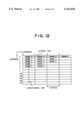
- FIG. 11 represents such a diagram that addresses are allocated to a memory having a 4-byte data width in correspondence with a paper. While such an address-allocated memory is used, when 128 dots of a lateral line of this figure are expanded along the X direction, and 128 dots of a longitudinal line thereof are expanded along the Y direction, the resultant expanding process time of the former dot expansion is completely different from that of the latter dot expansion. The reason is given as follows. When as a memory capable of processing 32-dot data in a batch manner, a DRAM is employed, since a page mode access operation is available within a page boundary, in which only a column address is switched, the highspeed data access operation can be achieved. To the contrary, since the data access operation is carried out by switching the memory address every 1 dot along the Y direction, the expanding process operation is delayed.
- FIG. 12 is a conceptual diagram for schematically explaining a conventional memory access control system such as that disclosed in JP-A-61-80339.
- a conventional memory access control system such as that disclosed in JP-A-61-80339.
- the memory banks are switched.
- the dot data can be expanded in a higher speed than that of the memory access control system shown in FIG. 11. Since the memory banks are switched every time the X address and the Y address are changed, a difference between the expanding performance in the X direction and the expanding performance in the Y direction will depend on the effect of the data widths.
- a memory access control method In a memory access control method, according to an aspect of the present invention, there are provided a plurality of memories whose address mapping is logically, or physically different from each other. In response to a directivity of address changes in a data set such as bit map data accessible to these memories, such a memory having address mapping, the accessing time of which is shorter than other memories, is selected to be accessed.
- a memory access control apparatus is featured by comprising: a plurality of memories, the address mapping of which is logically, or physically different from each other, and which are managed by a two-dimensional address constructed of a first address and a second address; an address changing apparatus for mutually changing the first address and the second address; a judging apparatus for judging a directivity of address changes in a data set continuously accessible to the memories; and a selecting apparatus for selecting the memories accessed, depending upon sorts of the directivity.
- the memory access control apparatus may be constituted by employing a memory logic hybrid LSI made by that these plural memories, and a control logic capable of realizing at least one of the address changing means, the judging means, and the selecting means are packaged with the same LSI chip.
- the memory access control method has such an effect that a memory access technique is capable of accessing in a high speed the memory managed by the two-dimensional address regardless of the directivity of address changes which occur during the access operation, and of realizing the continuous access operation of the data set such as the bit map.
- the memory access control method owns another effect that a memory access control technique is capable of controlling the full dot memory managed by the two-dimensional address, in which the bit map of the arbitrary figure can be expanded in a high speed.
- the memory access control apparatus has such an effect that a memory access technique is capable of accessing in a high speed the memory managed by the two-dimensional address regardless of the directivity of address changes which occur during the access operation, and of realizing the continuous access operation of the data set such as the bit map.
- the memory access control apparatus has such an effect that a memory access control technique is capable of controlling the full dot memory managed by the two-dimensional address, in which the bit map of the arbitrary figure can be expanded in a high speed.
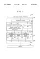
- FIG. 1 is a conceptional diagram for representing an example of an arrangement of a printing system containing a printer control apparatus to which a memory access control method and a memory access control apparatus, according to one embodiment of the present invention, have been applied;
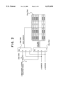
- FIG. 2 is a conceptional diagram for indicating an example of a memory for constituting a full dot memory employed in a printer control apparatus to which the memory access control method and the memory access control apparatus, according to one embodiment of the present invention, have been applied;
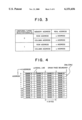
- FIG. 3 is a conceptional diagram for representing an example of effects of a control signal used in the printer control apparatus to which the memory access control method and the memory access control apparatus, according to one embodiment of the present invention, have been applied:
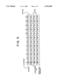
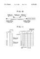
- FIG. 4 is a conceptional diagram for indicating an example of the memory for constituting the full dot memory employed in the printer control apparatus to which the memory access control method and the memory access control apparatus, according to one embodiment of the present invention, have been applied;
- FIG. 5 is a conceptional diagram for indicating an example of the memory for constituting the full dot memory employed in the printer control apparatus to which the memory access control method and the memory access control apparatus, according to one embodiment of the present invention, have been applied;
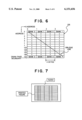
- FIG. 6 is a conceptional diagram for indicating an example of the memory for constituting the full dot memory employed in the printer control apparatus to which the memory access control method and the memory access control apparatus, according to one embodiment of the present invention, have been applied;
- FIG. 7 is a conceptional diagram for indicating an example of print data expanded in the full dot memory employed in the printer control apparatus to which the memory access control method and the memory access control apparatus, according to one embodiment of the present invention, have been applied;
- FIG. 8 is a conceptional diagram for indicating an example of a dot pattern expanded from the print data expanded in the full dot memory employed in the printer control apparatus to which the memory access control method and the memory access control apparatus, according to one embodiment of the present invention, have been applied;
- FIG. 9 is a conceptional diagram for showing an example of a sort judging condition for the dot pattern used in the memory access control method and the memory access control apparatus, according to one embodiment of the present invention.
- FIG. 10 is a conceptional diagram for showing an example of a sort judging condition for the dot pattern used in the memory access control method and the memory access control apparatus, according to one embodiment of the present invention.
- FIG. 11 is a conceptional diagram for indicating one example of expanding of a dot pattern for a memory with a two-dimensional address.
- FIG. 12 is a conceptional diagram for showing one example of the conventional memory access control system.
- FIG. 1 is a conceptional diagram for representing an example of an arrangement of a printing system involving a printer control apparatus, to which a memory access control method and a memory access control apparatus, according to an embodiment mode of the present invention have been applied.
- DRAM dynamic random access memory
- SRAM static random access memory
- a printing system is arranged by a host-sided channel apparatus 100, a printer control apparatus 200, and a printer 300.
- the printer control apparatus 200 is constituted by an intermediate buffer 210, a data processing processor 220, a full dot memory 230, a selector 240, and so on.
- the printer control apparatus 200 which is constituted by the intermediate buffer 210, the data processing processor 220, the full dot memory 230, and the memory 240, may be arranged by employing, for instance, such a memory logic hybrid LSI made by that a memory element for constituting the intermediate buffer 210 and the full dot memory 230, and also a control logic circuit capable of realizing the data processing processor 220 having a control function (will be discussed later) and the selector 240 are packaged on the same LSI chip.
- the data processing processor 220 contains a data processing unit 221, a memory control unit 224, a bus 225 for a dot pattern, a parameter setting unit 222 and another parameter setting unit 223, into which parameter information such as a threshold value and used to control operations of the memory control unit 224 (will be discussed later) is set.
- These parameter setting units 222 and 223 are arranged as a register and the like accessible by the memory control unit 224 in such a manner that, for instance, a setting command issued from a host-sided (upper-graded) channel apparatus 100, and an externally supplied content are arbitrarily set via a control panel (not shown) connected to the printer control apparatus 200.
- the full dot memory 230 includes exclusively-used memories called as a longitudinal/lateral-direction highspeed memory 234(1) managed by a two-dimensional address, an oblique-direction highspeed memory 235, and another longitudinal/lateral-direction highspeed memory 236(2).
- the full dot memory 230 with such an arrangement is constituted by, for example, a two-plane structure of a memory plane 230A and another memory plane 230B. Then, a plurality of pages can be continuously printed by alternately executing a data reading operation and a data writing operation in a parallel manner without an occurrence of a waiting state of printing operation by a printer 300, which is caused by a waiting state until the data writing operation to the full dot memory 230 is completed.
- print data for a preceding page is read from one memory plane 230A(B) to the printer 300.
- print data for a succeeding page is written from the data processing processor 220 to the other memory plane 230B(A).
- each of these longitudinal/lateral-direction highspeed memories 234(1) and 236(2) is constituted by a memory medium 234a (memory medium 236a) with a plural bank structure; a plurality of selector 234b (selector 236b) and selector 234c (selector 236c) capable of executing an operation for alternately changing corresponding relationships with respect to a row address/a column address in the memory medium 234a (memory medium 236a) of the x address and y address; and an inverter 234d (inverter 236d) for causing the selecting operations of the selector 234b (selector 236b) and the selector 234c (selector 236c) to be mutually inverted in response to a longitudinal/lateral selection signal "S" equal to a common logic signal.
- a longitudinal/lateral selection signal "S" equal to a common logic signal.
- FIG. 2 illustrates the two-bank structure along the column address direction in the memory medium 234a (memory medium 236a) with the plural bank structure.
- this memory medium 234a, or the memory medium 236a may be arranged by an n-bank structure, and symbol "n" is a natural number larger than, or equal to 3.
- the oblique-direction highspeed memory 235 is so arranged by that 4 bytes (namely 32 bits) of different banks are accessed along the x-address direction every time this x address is changed, whereas 1 bit within the same bank is accessed along the y-address direction.
- FIG. 6 shows the two-bank structure along the x address (row address) direction in the oblique-direction highspeed memory 235.
- this oblique-direction highspeed memory 235 may be arranged by an n-bank structure, and symbol "n" is equal to a natural number larger than, or equal to 3.
- the print data sent from the host-sided channel apparatus 100 to the printer control apparatus 200 is acquired by the intermediate buffer 210 employed in the printer control apparatus 200.
- This print data is expanded to a dot pattern (bit pattern) by the data processing unit 221 employed in the data processing processor 220, and then the dot pattern is written into the full dot memory 230.
- the full dot memory 230 is arranged by such an exclusively-used memory as the longitudinal/lateral-direction highspeed memory 234(1), the oblique-direction highspeed memory 235, and the longitudinal/lateral-direction highspeed memory 236(2).
- the longitudinal/lateral-direction highspeed memory 234(1) and the longitudinal lateral-direction highspeed memory 236(2) are made by the completely same memory structures, and are operable in different manners in response to the longitudinal/lateral selection signal S.
- this memory control unit 224 may judge as to which exclusively-used memory is accessed/selected. For instance, when the memory control unit 224 judges that a certain dot pattern corresponds to an x component, the longitudinal/lateral-direction highspeed memory 234(1) is accessed. Also, when the memory control unit 224 judges that a certain dot pattern corresponds to an xy component (oblique component), the oblique-direction highspeed memory 235 is accessed. Further, when the memory control unit 224 judges that a certain dot pattern corresponds to a y component, the longitudinal/lateral-direction highspeed memory 236(2) is accessed. These access operations are classified to be stored.
- the memory control unit 224 manages the x addresses and the y addresses of the respective exclusively-used memories based on the coordinate values corresponding to papers, and enters these x address and y address via an address line 231, an address line 232, and an address line 233 into the respective exclusively-used memories.
- the memory regions within each of the exclusively-used memories are banked, and when an access exceeding a page boundary of the DRAM is produced, different banks are accessed in a parallel manner, so that these exclusively-used memories can be accessed in high speeds.
- the exclusively-used memories own a read modify write function, and a read/clear function.
- the dot patterns saved in the respective exclusively-used memories may be directly supplied via a selector 240 to the printer 300 for the printing operation.
- FIG. 7 is an explanatory diagram for illustrating a figure in which figure elements having different directivities are mixed, for instance, a table, a ruled line, and the like being printed on a paper.
- FIG. 8 is an explanatory diagram for illustrating such an example that this figure (dot pattern) of FIG. 7 is dissolved into a component along the x direction and another component along the y direction.
- the figures such as the table and the ruled line as shown in FIG. 7 are supplied from the host-sided (upper-graded) channel apparatus 100 as the print data made of vector data about a plurality of line segments. The coordinate values of the both ends of these line segments, and widths thereof are designated.
- the data processing unit 221 the following writing operation is carried out. That is, a dot pattern for constituting a lateral line and a longitudinal line illustrated in FIG. 8 is separately produced from the vector data of each of these line segments, and then the dot pattern is written into the full dot memory 230 in the data processing unit 221.
- the x component (lateral line) can be expand-processed in the high speed, whereas when the y component (longitudinal line) is frequently produced, the lengthy memory access time is required when the dot pattern is expanded, resulting in lowering of the printing performance.
- no continuous printing operation can be done by the conventional printer control apparatus.
- the printer 300 is stopped, since the printer 300 should wait the completion of the data writing operation into the full dot memory 230 every time one page is printed out, resulting in lowering of the printing speed thereof.
- the exclusively-used memories in which the address mapping operations are different from each other, depending upon the exchange of the x address and the y address, are selectively used in response to the x component and the y component, so that the highspeed memory access control can be achieved.
- FIG. 4 represents such a longitudinal/lateral-direction highspeed memory 234(1) which is arranged by a DRAM having a 4-byte data width address-mapped in correspondence with a paper, and in which a writing operation for x-direction component can be carried out in high speed.
- a lateral line (dot pattern) constructed of 128 dots is expanded along the X direction into this longitudinal/lateral-direction highspeed memory 234(1), since this highspeed memory 234(1) can be accessed in unit of 4 bytes, the entire 128 dots can be expanded by performing the access operations 4 times.
- the memory region is subdivided into the plural banks in order that while a memory of a certain bank is being accessed, another bank access operation can be done, so that the y address is made in a high speed. If the longitudinal/lateral direction highspeed memory 234(1) with such an address mapping system is employed, the x component (lateral line) shown in FIG. 8 can be expanded in a high speed, as previously explained.
- FIG. 5 represents such a longitudinal/lateral-direction highspeed memory 236(2) which is arranged by a DRAM having a 4-byte data width address-mapped in correspondence with a paper, and in which a writing operation for y-direction component can be carried out in high speed.
- a longitudinal line (dot pattern) constructed of 128 dots is expanded along the y direction into this longitudinal/lateral-direction highspeed memory 236(2), since this highspeed memory 236(2) can be accessed in unit of 4 bytes, the entire 128 dots can be expanded by performing the access operations 4 times.
- the memory region is subdivided into the plural banks in order that while a memory of a certain bank is being accessed, another bank access operation can be done, so that the x address is made in a high speed. If the longitudinal/lateral direction highspeed memory 236(2) with such an address mapping system is employed, the y component (longitudinal line) can be expanded in a high speed, as previously explained.
- the longitudinal/lateral-direction highspeed memory 234(1) and the longitudinal/lateral-direction highspeed memory 236(2) with the different address mapping systems as indicated in FIG. 4 and FIG. 5 may be realized by merely changing the longitudinal/lateral selection signal S, with employment of the common memory structure as indicated in FIG. 2.
- a selector 234b (236b) and a selector 234c (236c) are provided between a row address and a column address of the memory medium 234a (memory medium 236a), and between an x address and a y address thereof, and a "longitudinal/lateral selection signal S" defined when a component of a dot pattern is judged is applied as a condition for switching the selector 234b (236b) and the selector 234c (236c).
- the row address, the column address, the x address, and the y address can be simply converted.
- FIG. 3 represents one example of a conversion relationship between the logic state of the longitudinal/lateral selection signal S, and the memory addresses (row addresses, column address), and also the real addresses (x address, y address).
- the longitudinal/lateral selection signal S when the longitudinal/lateral selection signal S is equal to "0", the row address of the memory is the y address and the column address thereof is the x address.
- the longitudinal/lateral selection signal S is equal to "1"
- the row address of the memory is the x address and the column address thereof is the x address.
- This judgment condition represented in FIG. 9 may be expressed by the following formulae (1) and (2), assuming that the starting-point coordinate is (x1, y1), and the end-point coordinate is (x2, y2):
- the expanding process operation of the print data eccentrically containing the x components, and also the expanding process operation of the print data eccentrically containing the y components can be carried at in a high speed.
- an oblique-direction highspeed memory 235 with a memory structure (address mapping) as indicated in FIG. 6 is further employed as an oblique-line exclusively used memory.
- this memory structure of FIG. 6 since the y components are accessed every 1 dot, the highspeed access operation can be realized by the page mode of the DRAM (namely, access operation is performed by that row address is fixed and only column address is switched).
- the highspeed access operation for the x components can be realized by way of the effect for banking the data width and the memory.
- a dot pattern-expanded in the data processing unit 221 corresponds to an x component, a y component, or an oblique component.
- this judgment is performed in the memory control unit 224 based on a judgment condition represented in FIG. 10.
- a coordinate value of a starting point of a dot pattern expanded in the data processing unit 221 of FIG. 1 is set to (x1, y1), and a coordinate value of an end point of this dot pattern is set to (x2, y2).
- the selection bases for selecting any of the respective exclusively-used memories namely the longitudinal/lateral-direction highspeed memory 234(1), the oblique-direction highspeed memory 235, and the longitudinal/lateral-direction highspeed memory 236(2) are different from each other, depending upon the characteristics of the memory elements for constituting these exclusively-used memories. Accordingly, parameters are set in order that these selection bases can be varied, and these parameters can be arbitrarily and externally set to the parameter setting units 222 and 223.
- the coordinate information about the starting point and the end point which are sent from the data processing unit 221 is calculated by the memory control unit 224, and then the parameter A set to the parameter setting unit 222 is compared with the parameter B set to the parameter setting unit 223, so that it is possible to judge as to whether this dot pattern corresponds to the x component, the y component, or the xy component (oblique component).
- the judgment condition of FIG. 10 may be expressed by the below-mentioned formulae (3), (4), and (5):
- the full dot memory 230 managed by the two-dimensional address is arranged by the respective exclusively-used memories such as the longitudinal/lateral-direction highspeed memory 234(1), the oblique-direction highspeed memory 235, and the longitudinal/lateral-direction highspeed memory 236(2).
- the component of this dot pattern is judged.
- changing of the x address and the y address is controlled which are supplied via the address lines 231, 232, 233 to the respective exclusively-used memories, if required, and also one of these exclusively-used memories is selected.
- the occurrence of the expanding performance (expand requiring time) time can be avoided which is caused by such a fact that the expanding direction of the dot pattern is different from the address mapping of the memories. Also, the time required to access the memories can be shortened, and further the memory accessible number within a predetermined time period can be increased.
- the dot data can be expanded from the print data into the full dot memory 230 in a high speed in such a case that the dot data expanded from this print data received from the host-sided channel apparatus 100 is expanded into the full-dot memory 230.
- this expanded dot data corresponds to the x component (lateral line) shown in the left side of FIG. 8, the y component (longitudinal line) indicated in the right side of FIG. 8, or the xy component (oblique line) indicated in other portions of FIG.
- a selection can be made of the longitudinal/lateral-direction highspeed memory 234(1), the longitudinal/lateral-direction highspeed memory 236(2), and the oblique-direction highspeed memory 235, in which the time required to write the relevant dot data is the shortest writing time. Then, the relevant dot data can be written into the selected highspeed memory.
- the delays of the printing operation can be avoided and thus the printing operation can be done in the high throughput.
- the delays of the printing operation are caused by that the printer 300 is stopped until the dot data expansion to the full dot memory 230 is completed.
- the printer control apparatus 200 is arranged by the memory logic hybrid LSI, the printer control apparatus 200 can be considerably made compact, operable under high speed, and also low power consumption.
- the memory elements for constructing the intermediate buffer 210 and the full dot memory 230, and also the data processing processor 220 having the control function (will be discussed later) and the control logic capable of realizing the selector 240 are mounted, or packaged on the same LSI chip.
- a memory logic hybrid LSI owns the following three features by mounting a control LSI and a memory on a printed circuit board in a mixture manner, although these control LSI and memory are conventionally and separately mounted in a printed circuit board.
- the memory access control method/apparatus of the present invention may be applied not only to the full dot memory employed in the print control apparatus, but also may be applied to general-purpose memories which are widely used so as to expand bit map data such as graphic data outputted on a display.
Abstract
Description
|(x2-x1)|-|(y2-y1)|≧0(1)
|(x2-x1)|-|(y2-y1)|<0 (2)
|(x2-x1)|-|(y2-y1)|≧parameter B(3)
parameter A≦|(x2-x1)|-|(y2-y1)|<parameter B (4)
|(x2-x1)|-|(y2-y1)|<parameter A(5)
Claims (4)
Applications Claiming Priority (2)
| Application Number | Priority Date | Filing Date | Title |
|---|---|---|---|
| JP9-048238 | 1997-03-03 | ||
| JP9048238A JPH10240613A (en) | 1997-03-03 | 1997-03-03 | Memory access control mehtod and device |
Publications (1)
| Publication Number | Publication Date |
|---|---|
| US6151656A true US6151656A (en) | 2000-11-21 |
Family
ID=12797875
Family Applications (1)
| Application Number | Title | Priority Date | Filing Date |
|---|---|---|---|
| US09/031,543 Expired - Fee Related US6151656A (en) | 1997-03-03 | 1998-02-27 | Memory apparatus and method for controlling memory access based on memory address directivity |
Country Status (2)
| Country | Link |
|---|---|
| US (1) | US6151656A (en) |
| JP (1) | JPH10240613A (en) |
Cited By (2)
| Publication number | Priority date | Publication date | Assignee | Title |
|---|---|---|---|---|
| US20090006807A1 (en) * | 2007-06-29 | 2009-01-01 | Novatek Microelectronics Corp. | Method for memory address arrangement |
| CN101344866B (en) * | 2007-07-11 | 2012-04-18 | 联詠科技股份有限公司 | Memory address arranging method |
Citations (8)
| Publication number | Priority date | Publication date | Assignee | Title |
|---|---|---|---|---|
| JPS6180339A (en) * | 1984-09-26 | 1986-04-23 | Hitachi Ltd | Memory access control system |
| US4683552A (en) * | 1983-04-27 | 1987-07-28 | Hitachi, Ltd. | System for on-line and off-line display |
| US4956717A (en) * | 1987-12-18 | 1990-09-11 | Hitachi, Ltd. | Method of and apparatus for controller duplex page printer |
| US4996650A (en) * | 1988-09-12 | 1991-02-26 | Hitachi Ltd. | Print control system |
| US5105472A (en) * | 1989-03-09 | 1992-04-14 | Noboru Murayama | Graphic reproduction method |
| US5210822A (en) * | 1990-11-28 | 1993-05-11 | Hitachi, Ltd. | Storage control system for print image data |
| US5413419A (en) * | 1992-03-16 | 1995-05-09 | Hitachi, Ltd. | Printer, a printer control system and method |
| US5754164A (en) * | 1994-06-29 | 1998-05-19 | Fujitsu Limited | Outline font expanding method and outline font expanding device |
-
1997
- 1997-03-03 JP JP9048238A patent/JPH10240613A/en active Pending
-
1998
- 1998-02-27 US US09/031,543 patent/US6151656A/en not_active Expired - Fee Related
Patent Citations (9)
| Publication number | Priority date | Publication date | Assignee | Title |
|---|---|---|---|---|
| US4683552A (en) * | 1983-04-27 | 1987-07-28 | Hitachi, Ltd. | System for on-line and off-line display |
| JPS6180339A (en) * | 1984-09-26 | 1986-04-23 | Hitachi Ltd | Memory access control system |
| US4752915A (en) * | 1984-09-26 | 1988-06-21 | Hitachi, Ltd. | Two dimensionally addressable memory apparatus with bank switching |
| US4956717A (en) * | 1987-12-18 | 1990-09-11 | Hitachi, Ltd. | Method of and apparatus for controller duplex page printer |
| US4996650A (en) * | 1988-09-12 | 1991-02-26 | Hitachi Ltd. | Print control system |
| US5105472A (en) * | 1989-03-09 | 1992-04-14 | Noboru Murayama | Graphic reproduction method |
| US5210822A (en) * | 1990-11-28 | 1993-05-11 | Hitachi, Ltd. | Storage control system for print image data |
| US5413419A (en) * | 1992-03-16 | 1995-05-09 | Hitachi, Ltd. | Printer, a printer control system and method |
| US5754164A (en) * | 1994-06-29 | 1998-05-19 | Fujitsu Limited | Outline font expanding method and outline font expanding device |
Cited By (3)
| Publication number | Priority date | Publication date | Assignee | Title |
|---|---|---|---|---|
| US20090006807A1 (en) * | 2007-06-29 | 2009-01-01 | Novatek Microelectronics Corp. | Method for memory address arrangement |
| US8245010B2 (en) * | 2007-06-29 | 2012-08-14 | Novatek Microelectronics | Method for memory address arrangement |
| CN101344866B (en) * | 2007-07-11 | 2012-04-18 | 联詠科技股份有限公司 | Memory address arranging method |
Also Published As
| Publication number | Publication date |
|---|---|
| JPH10240613A (en) | 1998-09-11 |
Similar Documents
| Publication | Publication Date | Title |
|---|---|---|
| KR0171487B1 (en) | Semiconductor integrated circuit device and image data processing system using it | |
| US8332683B2 (en) | Data processing system and image processing system | |
| US5781201A (en) | Method for providing improved graphics performance through atypical pixel storage in video memory | |
| US4752915A (en) | Two dimensionally addressable memory apparatus with bank switching | |
| US6151656A (en) | Memory apparatus and method for controlling memory access based on memory address directivity | |
| US5929871A (en) | Access control apparatus and image processing system | |
| US6674442B1 (en) | Image memory system | |
| US6014225A (en) | Frame buffer control method and circuit | |
| JPS62299892A (en) | Access system for character generator memory | |
| KR920003046B1 (en) | Character and pattern descripter | |
| JPH0764850A (en) | Painting-out plotter | |
| JP3070454B2 (en) | Memory access control circuit | |
| JP2590695B2 (en) | Time division switch circuit | |
| JPH0651750A (en) | Plotting device | |
| JP3005220B2 (en) | Scanning display controller | |
| JPH02108171A (en) | Frame memory device | |
| JP2001024180A (en) | Semiconductor integrated circuit device | |
| JPH0652328A (en) | Image processor | |
| JPH04239935A (en) | Controller for bit map memory | |
| JPH0812545B2 (en) | Pattern data output controller | |
| JP2000035915A (en) | Access controller of semiconductor memory | |
| JPH03147593A (en) | Bit block transfer device | |
| JPH10208028A (en) | Image data processor and image data storing method | |
| JPH07248965A (en) | Controller for image forming device | |
| JPH03134750A (en) | Dma data transfer device |
Legal Events
| Date | Code | Title | Description |
|---|---|---|---|
| AS | Assignment |
Owner name: HITACHI, LTD., JAPAN Free format text: ASSIGNMENT OF ASSIGNORS INTEREST;ASSIGNORS:MASHIMA, HAYATERU;AMARI, MITSUHIRO;REEL/FRAME:009275/0641 Effective date: 19980217 |
|
| FPAY | Fee payment |
Year of fee payment: 4 |
|
| AS | Assignment |
Owner name: RICOH PRINTING SYSTEMS, LTD., JAPAN Free format text: ASSIGNMENT OF ASSIGNORS INTEREST;ASSIGNOR:HITACHI, LTD.;REEL/FRAME:020054/0169 Effective date: 20061120 |
|
| FPAY | Fee payment |
Year of fee payment: 8 |
|
| FEPP | Fee payment procedure |
Free format text: PAYOR NUMBER ASSIGNED (ORIGINAL EVENT CODE: ASPN); ENTITY STATUS OF PATENT OWNER: LARGE ENTITY |
|
| REMI | Maintenance fee reminder mailed | ||
| LAPS | Lapse for failure to pay maintenance fees | ||
| STCH | Information on status: patent discontinuation |
Free format text: PATENT EXPIRED DUE TO NONPAYMENT OF MAINTENANCE FEES UNDER 37 CFR 1.362 |
|
| FP | Lapsed due to failure to pay maintenance fee |
Effective date: 20121121 |