US6150878A - Low voltage device operable with a high voltage supply - Google Patents
Low voltage device operable with a high voltage supply Download PDFInfo
- Publication number
- US6150878A US6150878A US09/005,604 US560498A US6150878A US 6150878 A US6150878 A US 6150878A US 560498 A US560498 A US 560498A US 6150878 A US6150878 A US 6150878A
- Authority
- US
- United States
- Prior art keywords
- transistors
- voltage
- integrated circuit
- gate oxide
- circuit device
- Prior art date
- Legal status (The legal status is an assumption and is not a legal conclusion. Google has not performed a legal analysis and makes no representation as to the accuracy of the status listed.)
- Expired - Fee Related
Links
Images
Classifications
-
- H—ELECTRICITY
- H10—SEMICONDUCTOR DEVICES; ELECTRIC SOLID-STATE DEVICES NOT OTHERWISE PROVIDED FOR
- H10D—INORGANIC ELECTRIC SEMICONDUCTOR DEVICES
- H10D89/00—Aspects of integrated devices not covered by groups H10D84/00 - H10D88/00
- H10D89/10—Integrated device layouts
-
- H—ELECTRICITY
- H10—SEMICONDUCTOR DEVICES; ELECTRIC SOLID-STATE DEVICES NOT OTHERWISE PROVIDED FOR
- H10D—INORGANIC ELECTRIC SEMICONDUCTOR DEVICES
- H10D84/00—Integrated devices formed in or on semiconductor substrates that comprise only semiconducting layers, e.g. on Si wafers or on GaAs-on-Si wafers
- H10D84/80—Integrated devices formed in or on semiconductor substrates that comprise only semiconducting layers, e.g. on Si wafers or on GaAs-on-Si wafers characterised by the integration of at least one component covered by groups H10D12/00 or H10D30/00, e.g. integration of IGFETs
- H10D84/82—Integrated devices formed in or on semiconductor substrates that comprise only semiconducting layers, e.g. on Si wafers or on GaAs-on-Si wafers characterised by the integration of at least one component covered by groups H10D12/00 or H10D30/00, e.g. integration of IGFETs of only field-effect components
- H10D84/83—Integrated devices formed in or on semiconductor substrates that comprise only semiconducting layers, e.g. on Si wafers or on GaAs-on-Si wafers characterised by the integration of at least one component covered by groups H10D12/00 or H10D30/00, e.g. integration of IGFETs of only field-effect components of only insulated-gate FETs [IGFET]
- H10D84/8314—Integrated devices formed in or on semiconductor substrates that comprise only semiconducting layers, e.g. on Si wafers or on GaAs-on-Si wafers characterised by the integration of at least one component covered by groups H10D12/00 or H10D30/00, e.g. integration of IGFETs of only field-effect components of only insulated-gate FETs [IGFET] the IGFETs characterised by having gate insulating layers with different properties
-
- H—ELECTRICITY
- H10—SEMICONDUCTOR DEVICES; ELECTRIC SOLID-STATE DEVICES NOT OTHERWISE PROVIDED FOR
- H10D—INORGANIC ELECTRIC SEMICONDUCTOR DEVICES
- H10D84/00—Integrated devices formed in or on semiconductor substrates that comprise only semiconducting layers, e.g. on Si wafers or on GaAs-on-Si wafers
- H10D84/90—Masterslice integrated circuits
Definitions
- the present invention relates to integrated circuit devices generally and more particularly to deep sub-micron devices.
- the present invention seeks to provide an improved integrated circuit device which overcomes the above-described limitations of the prior art.
- an integrated circuit device including transistors having predetermined upper voltage limits, a multi-layer metal interconnect structure connecting the transistors to each other and to an external voltage source having a voltage in excess of the predetermined upper voltage limits of a first plurality of transistors, and a voltage reducer connected along the interconnect structure between the external voltage source and the first plurality of transistors.
- the integrated circuit device is a programmable device, such as field programmable gate array, mask programmable gate array or laser programmable gate array.
- the first plurality of transistors constitutes at least 50% of the total number of transistors in the integrated circuit device.
- the first plurality of transistors constitutes at least 90% of the total number of transistors in the integrated circuit device.
- the voltage reducer comprises an N-transistor having a source connected to the external voltage source, a gate connected via a voltage divider including a capacitor to the external voltage source and to ground and a drain connected to at least some of the first plurality of transistors.
- the voltage reducer comprises a plurality of voltage reducers which are generally uniformly distributed over a periphery of the integrated circuit device.
- the voltage reducer comprises a voltage reducer transistor
- the first plurality of transistors each comprise a first gate oxide and the voltage reducer transistor comprises a second gate oxide and wherein the second gate oxide is thicker than the first gate oxide.
- the first plurality of transistors constitutes at least 50% of the total number of transistors in the integrated circuit device.
- the first plurality of transistors constitutes at least 90% of the total number of transistors in the integrated circuit device.
- the external voltage source has a single output voltage which is in excess of the predetermined upper voltage limits of a first plurality of transistors.
- an integrated circuit device including transistors having predetermined upper voltage limits, a multi-layer metal interconnect structure connecting the transistors to each other and to an external voltage source having a single output voltage which is in excess of the predetermined upper voltage limits of a first plurality of the transistors, and a voltage reducer connected along the interconnect structure between the external voltage source and the first plurality of the transistors.
- the voltage reducer comprises an N-transistor having a source connected to the external voltage source, a gate connected to the external voltage source and to ground via a voltage divider including a capacitor and a drain connected to at least some of the first plurality of transistors.
- the first plurality of transistors each comprise a first gate oxide and the N-transistor comprises a second gate oxide and wherein the second gate oxide is thicker than the first gate oxide.
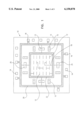
- FIG. 1 is a simplified illustration of an integrated circuit device constructed and operative in accordance with a preferred embodiment of the present invention
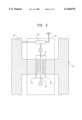
- FIG. 2 is a simplified illustration of a voltage reducer useful in the integrated circuit device of FIG. 1;
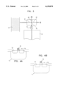
- FIG. 3 is a simplified illustration of a voltage divider useful in the voltage reducer of FIG. 2;
- FIGS. 4A and 4B are sectional illustrations of two different types of transistors employed in the integrated circuit of FIG. 1, showing the difference in the thickness of their respective oxide layers.
- FIG. 1 illustrates an integrated circuit device constructed and operative in accordance with a preferred embodiment of the present invention.
- the integrated circuit device comprises a semiconductor substrate 10 onto which are formed a multiplicity of transistors, including transistors 12 having a relatively low upper voltage limit and transistors 13, having a relatively high upper voltage limit.
- a first plurality of pads 14 which provide electrical signal connections to some of the transistors 13 which belong to I/O cells 15, and a second plurality of pads 16 which provide electrical power to the transistors 13.
- Pads 14 and 16 form part of a multilayer metal interconnect network 18 which also includes an outer, high voltage, metal ring 20 and an inner, low voltage, metal ring 22. It is noted that although in the illustrated embodiment, the pads 14 and 16 are shown at the periphery of the substrate, alternatively pads may be located at any other suitable location on the substrate.
- Pads 16 are connected to metal ring 20.
- Metal ring 20 is connected to metal ring 22 via multiple voltage reducers 25 which include some of transistors 13.
- Metal ring 22 powers transistors 12.
- Transistors 12 receive electrical signals from I/O cells 15.
- Metal ring 22 is not directly connected to any of pads 14 and 16.
- an N-transistor 30 includes a gate 32, a source 34 and a drain 36.
- the source 34 is connected to outer ring 20 (FIG. 1) and the drain is connected to inner ring 22 (FIG. 1).
- Gate 32 is connected via a voltage divider 38 to outer ring 20.
- N-transistor 30 has a relatively large W/L ratio, preferably exceeding 1000.
- N-transistor 30 may be implemented as a plurality of transistors connected in parallel.
- voltage divider 38 preferably comprises a resistor R1 40 connected between outer ring 20 and a junction 42, connected to gate 32 (FIG. 2), and a resistor R2 44 connected between junction 42 and ground.
- a capacitor 46 is connected between junction 42 and ground.
- the ratio of resistances of the resistors R1 and R2 must be determined in accordance with the following equation:
- VT is the threshold voltage of transistors 13 and VH is the voltage of the outer ring 20, pad 16 and of the external voltage source.
- FIGS. 4A and 4B are sectional illustrations of two different types of transistors employed in the integrated circuit of FIG. 1, showing the difference in the thickness of their respective oxide layers.
- a transistor 12 (FIG. 1) having a relatively low predetermined upper voltage limit, has a relatively thin gate oxide layer 50.
- a transistor 13 (FIG. 1), shown in FIG. 4B, has a relatively thick gate oxide layer 51.
- an example of the thickness of gate oxide layer 50 is 80 angstrom, while an example of the thickness of gate oxide layer 51 is 110 angstrom.
- transistors 12 and 13 may be identical, as indicated by identical reference numerals 52 indicating their sources, 54 indicating their drains and 56 indicating their gates.
- the present invention is particularly useful for operating 0.35 micrometer geometry integrated circuit devices in systems which supply only voltages of 5 volts, such as PCs and workstations, rather than at a voltage of 3.3 volts which is conventional for devices having this geometry. It is appreciated that for increasingly smaller geometries, even lower voltage limits apply for the transistors 12 and the present invention is equally applicable thereto.
Landscapes
- Metal-Oxide And Bipolar Metal-Oxide Semiconductor Integrated Circuits (AREA)
- Semiconductor Integrated Circuits (AREA)
Abstract
Description
R1/R2=[VH-(VL+VT)]/(VL+VT)
Claims (22)
Priority Applications (8)
| Application Number | Priority Date | Filing Date | Title |
|---|---|---|---|
| US09/005,604 US6150878A (en) | 1998-01-12 | 1998-01-12 | Low voltage device operable with a high voltage supply |
| CA002241440A CA2241440A1 (en) | 1998-01-12 | 1998-06-23 | Low voltage device operable with a high voltage supply |
| EP98810601A EP0929102A1 (en) | 1998-01-12 | 1998-06-29 | Low voltage device operable with a high voltage supply |
| SG9801565A SG81235A1 (en) | 1998-01-12 | 1998-07-01 | Low voltage device operable with a high voltage supply |
| JP10227465A JPH11214624A (en) | 1998-01-12 | 1998-08-12 | Low voltage devices that can be operated from high supply voltage sources |
| TW087113620A TW393757B (en) | 1998-01-12 | 1998-08-19 | Low voltage device operable with a high voltage supply |
| KR1019980033728A KR19990066744A (en) | 1998-01-12 | 1998-08-20 | Low Voltage Device Operates from High Voltage Supply |
| IL12752598A IL127525A0 (en) | 1998-01-12 | 1998-12-11 | Integrated circuit device |
Applications Claiming Priority (1)
| Application Number | Priority Date | Filing Date | Title |
|---|---|---|---|
| US09/005,604 US6150878A (en) | 1998-01-12 | 1998-01-12 | Low voltage device operable with a high voltage supply |
Publications (1)
| Publication Number | Publication Date |
|---|---|
| US6150878A true US6150878A (en) | 2000-11-21 |
Family
ID=21716714
Family Applications (1)
| Application Number | Title | Priority Date | Filing Date |
|---|---|---|---|
| US09/005,604 Expired - Fee Related US6150878A (en) | 1998-01-12 | 1998-01-12 | Low voltage device operable with a high voltage supply |
Country Status (8)
| Country | Link |
|---|---|
| US (1) | US6150878A (en) |
| EP (1) | EP0929102A1 (en) |
| JP (1) | JPH11214624A (en) |
| KR (1) | KR19990066744A (en) |
| CA (1) | CA2241440A1 (en) |
| IL (1) | IL127525A0 (en) |
| SG (1) | SG81235A1 (en) |
| TW (1) | TW393757B (en) |
Citations (4)
| Publication number | Priority date | Publication date | Assignee | Title |
|---|---|---|---|---|
| US4482985A (en) * | 1981-04-17 | 1984-11-13 | Hitachi, Ltd. | Semiconductor integrated circuit |
| US5309040A (en) * | 1989-11-07 | 1994-05-03 | Fujitsu Limited | Voltage reducing circuit |
| US5485117A (en) * | 1991-03-20 | 1996-01-16 | Fujitsu Limited | Power circuit and semiconductor device including the same |
| US5631547A (en) * | 1994-01-26 | 1997-05-20 | Fujitsu Limited | Power-supply-voltage reduction device, semiconductor integrated circuit device including the reduction device and method of producing electronic device including such devices |
Family Cites Families (5)
| Publication number | Priority date | Publication date | Assignee | Title |
|---|---|---|---|---|
| JPS5330283Y2 (en) * | 1973-07-19 | 1978-07-28 | ||
| US5493572A (en) * | 1981-04-17 | 1996-02-20 | Hitachi, Ltd. | Semiconductor integrated circuit with voltage limiter having different output ranges for normal operation and performing of aging tests |
| US5566185A (en) * | 1982-04-14 | 1996-10-15 | Hitachi, Ltd. | Semiconductor integrated circuit |
| JP2994522B2 (en) * | 1993-02-22 | 1999-12-27 | 富士通株式会社 | Preamplifier for magnetoresistive element |
| JP2775222B2 (en) * | 1993-09-14 | 1998-07-16 | ソニー・テクトロニクス株式会社 | Power control circuit |
-
1998
- 1998-01-12 US US09/005,604 patent/US6150878A/en not_active Expired - Fee Related
- 1998-06-23 CA CA002241440A patent/CA2241440A1/en not_active Abandoned
- 1998-06-29 EP EP98810601A patent/EP0929102A1/en not_active Withdrawn
- 1998-07-01 SG SG9801565A patent/SG81235A1/en unknown
- 1998-08-12 JP JP10227465A patent/JPH11214624A/en active Pending
- 1998-08-19 TW TW087113620A patent/TW393757B/en not_active IP Right Cessation
- 1998-08-20 KR KR1019980033728A patent/KR19990066744A/en not_active Ceased
- 1998-12-11 IL IL12752598A patent/IL127525A0/en unknown
Patent Citations (4)
| Publication number | Priority date | Publication date | Assignee | Title |
|---|---|---|---|---|
| US4482985A (en) * | 1981-04-17 | 1984-11-13 | Hitachi, Ltd. | Semiconductor integrated circuit |
| US5309040A (en) * | 1989-11-07 | 1994-05-03 | Fujitsu Limited | Voltage reducing circuit |
| US5485117A (en) * | 1991-03-20 | 1996-01-16 | Fujitsu Limited | Power circuit and semiconductor device including the same |
| US5631547A (en) * | 1994-01-26 | 1997-05-20 | Fujitsu Limited | Power-supply-voltage reduction device, semiconductor integrated circuit device including the reduction device and method of producing electronic device including such devices |
Also Published As
| Publication number | Publication date |
|---|---|
| JPH11214624A (en) | 1999-08-06 |
| IL127525A0 (en) | 1999-10-28 |
| CA2241440A1 (en) | 1999-07-12 |
| TW393757B (en) | 2000-06-11 |
| EP0929102A1 (en) | 1999-07-14 |
| KR19990066744A (en) | 1999-08-16 |
| SG81235A1 (en) | 2001-06-19 |
Similar Documents
| Publication | Publication Date | Title |
|---|---|---|
| JP2888898B2 (en) | Semiconductor integrated circuit | |
| US6489689B2 (en) | Semiconductor device | |
| KR100511808B1 (en) | Semiconductor integrated circuit and its fabrication method | |
| US4868705A (en) | Insulated-gate semicustom integrated circuit | |
| KR100382836B1 (en) | Current regulation semiconductor integrated circuit device and its manufacturing method | |
| US6858885B2 (en) | Semiconductor apparatus and protection circuit | |
| KR970004454B1 (en) | Semiconductor integrated circuit device | |
| KR100395880B1 (en) | Test element group structure | |
| US6140686A (en) | Semiconductor integrated circuit device | |
| US5825601A (en) | Power supply ESD protection circuit | |
| US6528853B2 (en) | Method and semiconductor structure for implementing dual plane body contacts for silicon-on-insulator (SOI) transistors | |
| US5892276A (en) | Semiconductor integrated circuit | |
| KR20040032755A (en) | Semiconductor integrated circuit device having a leakage current cutoff circuit, constructed using mt-cmos, for reducing standby leakage current | |
| JPH09213915A (en) | Integrated circuit chip with gate array book personalization using local interconnect | |
| US5332688A (en) | Method of manufacturing full CMOS type SRAM | |
| US6538293B2 (en) | Semiconductor integrated circuit device and method of manufacturing the same | |
| US5926064A (en) | Floating MOS capacitor | |
| US4786828A (en) | Bias scheme for achieving voltage independent capacitance | |
| US6150878A (en) | Low voltage device operable with a high voltage supply | |
| JP3883114B2 (en) | Semiconductor device | |
| US20030160285A1 (en) | Semiconductor device and method of manufacturing the same | |
| KR100363352B1 (en) | Sram memory cell | |
| US5856708A (en) | Polycide/poly diode SRAM load | |
| US20030137861A1 (en) | Semiconductor input/output circuit arrangement | |
| US5930191A (en) | Semiconductor memory device having a plurality of power voltages |
Legal Events
| Date | Code | Title | Description |
|---|---|---|---|
| AS | Assignment |
Owner name: CHIP EXPRESS (ISRAEL) LTD., ISRAEL Free format text: ASSIGNMENT OF ASSIGNORS INTEREST;ASSIGNORS:YOELI, UZI;ORBACH, ZVI;REEL/FRAME:011015/0372 Effective date: 19980104 |
|
| FEPP | Fee payment procedure |
Free format text: PAYOR NUMBER ASSIGNED (ORIGINAL EVENT CODE: ASPN); ENTITY STATUS OF PATENT OWNER: SMALL ENTITY |
|
| FPAY | Fee payment |
Year of fee payment: 4 |
|
| FEPP | Fee payment procedure |
Free format text: PAT HOLDER CLAIMS SMALL ENTITY STATUS, ENTITY STATUS SET TO SMALL (ORIGINAL EVENT CODE: LTOS); ENTITY STATUS OF PATENT OWNER: SMALL ENTITY |
|
| FPAY | Fee payment |
Year of fee payment: 8 |
|
| AS | Assignment |
Owner name: SILICON VALLEY BANK, CALIFORNIA Free format text: SECURITY INTEREST;ASSIGNOR:CHIPX, INC.;REEL/FRAME:026179/0023 Effective date: 20100423 |
|
| REMI | Maintenance fee reminder mailed | ||
| LAPS | Lapse for failure to pay maintenance fees | ||
| STCH | Information on status: patent discontinuation |
Free format text: PATENT EXPIRED DUE TO NONPAYMENT OF MAINTENANCE FEES UNDER 37 CFR 1.362 |
|
| FP | Lapsed due to failure to pay maintenance fee |
Effective date: 20121121 |
|
| AS | Assignment |
Owner name: CHIPX, INCORPORATED, CALIFORNIA Free format text: RELEASE BY SECURED PARTY;ASSIGNOR:SILICON VALLEY BANK;REEL/FRAME:041855/0702 Effective date: 20170404 |