US6150849A - Readout chip for nuclear applications - Google Patents
Readout chip for nuclear applications Download PDFInfo
- Publication number
- US6150849A US6150849A US08/866,117 US86611797A US6150849A US 6150849 A US6150849 A US 6150849A US 86611797 A US86611797 A US 86611797A US 6150849 A US6150849 A US 6150849A
- Authority
- US
- United States
- Prior art keywords
- integrated circuit
- signal
- readout
- channels
- data readout
- Prior art date
- Legal status (The legal status is an assumption and is not a legal conclusion. Google has not performed a legal analysis and makes no representation as to the accuracy of the status listed.)
- Expired - Lifetime
Links
- 230000001960 triggered effect Effects 0.000 claims description 6
- NJPPVKZQTLUDBO-UHFFFAOYSA-N novaluron Chemical compound C1=C(Cl)C(OC(F)(F)C(OC(F)(F)F)F)=CC=C1NC(=O)NC(=O)C1=C(F)C=CC=C1F NJPPVKZQTLUDBO-UHFFFAOYSA-N 0.000 claims description 5
- 238000012545 processing Methods 0.000 claims description 3
- 238000012360 testing method Methods 0.000 description 10
- XUIMIQQOPSSXEZ-UHFFFAOYSA-N Silicon Chemical compound [Si] XUIMIQQOPSSXEZ-UHFFFAOYSA-N 0.000 description 8
- 229910052710 silicon Inorganic materials 0.000 description 8
- 239000010703 silicon Substances 0.000 description 8
- 230000010354 integration Effects 0.000 description 7
- 229910004611 CdZnTe Inorganic materials 0.000 description 3
- 239000003990 capacitor Substances 0.000 description 3
- 238000002474 experimental method Methods 0.000 description 3
- 238000003384 imaging method Methods 0.000 description 3
- 238000000034 method Methods 0.000 description 3
- 239000002245 particle Substances 0.000 description 3
- 230000005855 radiation Effects 0.000 description 3
- 239000007787 solid Substances 0.000 description 3
- 238000002083 X-ray spectrum Methods 0.000 description 2
- 238000010586 diagram Methods 0.000 description 2
- 238000005516 engineering process Methods 0.000 description 2
- 239000000463 material Substances 0.000 description 2
- 239000004065 semiconductor Substances 0.000 description 2
- 229910000980 Aluminium gallium arsenide Inorganic materials 0.000 description 1
- JBRZTFJDHDCESZ-UHFFFAOYSA-N AsGa Chemical compound [As]#[Ga] JBRZTFJDHDCESZ-UHFFFAOYSA-N 0.000 description 1
- 229910004613 CdTe Inorganic materials 0.000 description 1
- 241000723353 Chrysanthemum Species 0.000 description 1
- 235000005633 Chrysanthemum balsamita Nutrition 0.000 description 1
- 229910001218 Gallium arsenide Inorganic materials 0.000 description 1
- 229910000530 Gallium indium arsenide Inorganic materials 0.000 description 1
- BUGBHKTXTAQXES-UHFFFAOYSA-N Selenium Chemical compound [Se] BUGBHKTXTAQXES-UHFFFAOYSA-N 0.000 description 1
- 238000003491 array Methods 0.000 description 1
- ZAIPMKNFIOOWCQ-UEKVPHQBSA-N cephalexin Chemical compound C1([C@@H](N)C(=O)N[C@H]2[C@@H]3N(C2=O)C(=C(CS3)C)C(O)=O)=CC=CC=C1 ZAIPMKNFIOOWCQ-UEKVPHQBSA-N 0.000 description 1
- 239000000919 ceramic Substances 0.000 description 1
- 230000007123 defense Effects 0.000 description 1
- 230000003111 delayed effect Effects 0.000 description 1
- 238000013461 design Methods 0.000 description 1
- 230000001066 destructive effect Effects 0.000 description 1
- 238000001514 detection method Methods 0.000 description 1
- 238000011161 development Methods 0.000 description 1
- 239000003814 drug Substances 0.000 description 1
- 230000000694 effects Effects 0.000 description 1
- 230000007613 environmental effect Effects 0.000 description 1
- 238000011156 evaluation Methods 0.000 description 1
- 238000010304 firing Methods 0.000 description 1
- 229910052732 germanium Inorganic materials 0.000 description 1
- GNPVGFCGXDBREM-UHFFFAOYSA-N germanium atom Chemical compound [Ge] GNPVGFCGXDBREM-UHFFFAOYSA-N 0.000 description 1
- RQQRAHKHDFPBMC-UHFFFAOYSA-L lead(ii) iodide Chemical compound I[Pb]I RQQRAHKHDFPBMC-UHFFFAOYSA-L 0.000 description 1
- 238000004519 manufacturing process Methods 0.000 description 1
- YFDLHELOZYVNJE-UHFFFAOYSA-L mercury diiodide Chemical compound I[Hg]I YFDLHELOZYVNJE-UHFFFAOYSA-L 0.000 description 1
- 230000002028 premature Effects 0.000 description 1
- 229910052711 selenium Inorganic materials 0.000 description 1
- 239000011669 selenium Substances 0.000 description 1
- 230000035945 sensitivity Effects 0.000 description 1
- 230000036962 time dependent Effects 0.000 description 1
Images
Classifications
-
- G—PHYSICS
- G01—MEASURING; TESTING
- G01J—MEASUREMENT OF INTENSITY, VELOCITY, SPECTRAL CONTENT, POLARISATION, PHASE OR PULSE CHARACTERISTICS OF INFRARED, VISIBLE OR ULTRAVIOLET LIGHT; COLORIMETRY; RADIATION PYROMETRY
- G01J1/00—Photometry, e.g. photographic exposure meter
- G01J1/42—Photometry, e.g. photographic exposure meter using electric radiation detectors
- G01J1/44—Electric circuits
Definitions
- the present invention relates generally to data acquisition systems, and more particularly to a front end electronics readout chip.
- Room temperature radiation detectors are the driving force behind the current effort to develop II-VI semiconductor materials.
- a room temperature, position-sensitive, high resolution technology such as silicon strip, silicon drift, or silicon pixel detectors coupled to dedicated readout electronics may fill many of the demands of the new detection applications and push radiation imaging to a new level of resolution and flexibility.
- the ASIC chips developed for high energy physics experiments cannot be used for most commercial applications such as medical and industrial imaging where an external trigger signal is unavailable.
- a front end electronics readout mixed signal ASIC chip normally has a large number of identical channels within a single monolithic chip.
- the channel number typically ranges from 4 to 256. Newer versions with more channels may be fabricated as narrower (i.e., less than 1 micrometer) processing capabilities become available.
- One of the principal benefits of these chips is the ability to handle the readout from detectors with extremely large numbers of channels. Because these chips can amplify minute amounts of charge produced by the detectors they are subject to noise problems. In order to reduce the noise, the chips are typically mounted very close to the detector element, strip, pad, or pixel. The detector elements, strips, pads, or pixels are then connected directly or indirectly with the shortest possible length to the input of the ASIC chip. The power supply rails have to be bypassed very close to the ASIC chip as well.
- the control and output signals are connected to control electronics which controls and interfaces the ASIC chip to the host computer.
- the present invention provides a front end multi-channel readout chip which can be used with a variety of different detectors.
- Each channel of the readout chip consists of an analog section which provides analog output signals on an A (i.e., analog) bus, and a digital section which provides fast trigger signals on a T (i.e., trigger) bus.
- Input from a detector goes directly into a low noise charge sensitive preamplifier 103.
- the output of the preamplifier goes into a polarity switching circuit and then an amplifier with gain.
- the next stage is a shaper amplifier with a variable peaking time followed by a peak hold (peak detect) circuit.
- the output of the peak hold circuit goes into two comparators.
- the first comparator is a low level discriminator and produces the trigger signal.
- the second comparator provides a higher level discriminator than the first. Therefore the second comparator can be used to reject events that produce a signal above a set pulse height.
- the signals from the first comparator from all the channels are sent to a separate OR circuit to produce the external trigger output.
- the trigger output signals the external readout interface that an event has occurred and provides an accurate timing of the event.
- readout modes for the preferred embodiment of the chip, some of which are: (i) a sparse readout mode which allows the readout of only the input channels that have a signal; (ii) a nearest neighbor readout mode which allows the readout of the detector strips with a signal and the two nearest neighbors; (iii) an all channel readout mode which allows the readout of all the channels of the chip in sequence; (iv) a global trigger mode; (v) an external delay mode; and (vi) a force enable mode which continuously connects any selected channel to the analog output.
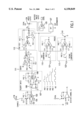
- FIG. 1 is an illustration of a circuit diagram of one of a plurality of detector channels.
- FIG. 1 may be one of 32 channels according to the invention.
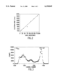
- FIG. 2 graphically illustrates the measured RMS electron noise versus the input capacitance of a chip fabricated according to the invention.
- FIG. 3 is a preliminary 241 Am x-ray spectrum from a CdZnTe detector.
- the readout chip of the present invention is designed as a mixed signal ASIC CMOS chip. Although the preferred embodiment of the chip has 32 detector channels, the same basic design can be used with either fewer or greater numbers of channels (i.e., 4, 8, 16, 32, 128, 256, etc.). Most of the solid state and/or semiconductor detectors such as silicon strip, silicon pixel, silicon drift, silicon PIN photodiodes, germanium, CdZnTe, CdTe, selenium, PbI 2 , GaAs, AlGaAs, InGaAs, HgBrI, and HgI 2 strip, pad, or pixel position sensitive detectors can be used with the present invention. Both single detectors as well as arrays of individual detectors can be used with the readout chip of the present invention.
- FIG. 1 is an illustration of a circuit diagram for the preferred embodiment of the invention in which only one channel is shown.
- An input 101 is single ended with an input amplifier 103 referenced to an external reference voltage source 105 that was measured to have an RMS noise level less than 1 microvolt a capacitor CDET connected to input 101 is the detector.
- a polarity switching circuit 107 including another gain stage 109.
- the polarity switching circuit 107 allows the chip to accept either positive or negative charge pulses (either positive or negative input polarities can be selected by using the negative ("-") or positive ("+”) inputs of the second stage amplifier 109, which is controlled by an externally supplied bit in the shift register.
- the next stage in the analog-chain is a shaper 111 in which time constants from 0.4 to 6 microseconds can be selected via three shift register data bits (8 selections from 0.4 to 8 microseconds).
- a peak hold circuit 113 follows the shaper and is connected to two threshold comparators 115 and 117.
- First comparator 115 can be considered to be a lower level discriminator which only allows an output trigger if the peak hold output is larger than the first applied threshold voltage 121.
- Second comparator 117 issues a signal if the peak hold output is larger than the second applied threshold voltage 123 but does not effect the output trigger of the chip and can be thought of as an upper level threshold indicator.
- Each of the 32 channels' peak hold outputs are multiplexed to a single analog output buffer 125 on a bus 124.
- a differentiator circuit may be placed in front of one or more comparators to produce one or more fast trigger outputs with low jitter for timing purposes for use in the external circuit.
- One or more special purpose channels may be placed into the chip to measure the pedestal and noise levels. These channels may be read out separately or at the same time with the normal channels to record the pedestal or background levels at that time within or outside the chip. These channels may also be used for differential signal inputs from one or more detectors.
- a test/calibration input 119 is coupled to the input of all of the channels. Input 119 is used to test and calibrate the readout chip.
- the readout chip of the present invention has several different readout modes. In the SPARSE mode only channels that are enabled and triggered are read out. In the GLOBAL TRIGGER mode all channels that are enabled are read out after any channel gets triggered. The SELECT ALL mode allows an external trigger to initiate readout of all enabled channels at any time. Nominally once a channel is triggered the rest of the channels get disabled within 2 to 50 nanoseconds. In the EXTERNAL DELAY mode the time after the initial trigger in which the other channels are disabled is controlled by an external input signal. In NEAR NEIGHBOR mode the nearest (adjacent) neighbors will also be read out together with the channel which produced the trigger. For diagnostic purposes there is a FORCE ENABLE mode that continuously connects a selectable single channel to the analog output. Up to sixteen readout chips according to the present invention may be daisy chained together.
- FIG. 2 is a graph of the output noise in electrons RMS versus input capacitance for a chip according to the present invention. This test was done using the calibration pulse input feature and connecting different capacitance values on the input. The slope of the line yields a figure of 8.3 electrons per picofarad and intercepts the y-axis for zero capacitance at 340 electrons RMS. The large offset of 340 electrons RMS may be due to the fact that the capacitors were coupled to the chip through 1 centimeter of trace on a ceramic carrier and about 3 centimeters on a printed circuit board made of FR4.
- FIG. 3 is a 241AM x-ray spectrum for a 3 ⁇ 3 ⁇ 2 mm 3 CdZnTe detector used in conjunction with a readout chip according to the present invention.
- the 59.5 keV peak has a width of about 400 electrons RMS.
Abstract
Description
______________________________________
Process          1.2 μm low noise CMOS process
   or other processes
  Number of channels 32 (readout chips may be daisy
   chained to form a large
   number of channels)
  Chip size About 0.5 cm.sup.2 or larger
  Bonding pitch 200 μm
  Integration time 8 selections from 400 ns to
  (Peaking time) 6 μs (other ranges possible)
  Data readout time Dependent upon integration time
  (first channel) (≈5 μs for 400 ns integration)
  Noise Approx. 100 electrons RMS at 6
   μs for 0 pf input capacitance
   or 550 electrons RMS at 6 μs
   for 40 pF input capacitance
  Power consumption Approximately 3 mW/channel
  Linear dynamic range Analog branch: noise level to
   150 ke (other ranges possible)
  Input polarity Both positive and negative
   input polarity can be selected
  Low level trigger output Range ≦220 keV. Walk ≈ 20 ns
                   at 400 ns integration time
   (other ranges possible)
  High level trigger output Range ≦600 keV (other ranges
   possible)
  Trigger output implementation OR of the output of 32
   comparators
  Comparator level adjust Both comparator levels are
   externally adjustable. Range
   of adjustment: noise level to
   range given above.
  Trigger level drift Stable to about 1% of trigger
   range
  Cross talk ≦1%
  Dark current drift Provision is built into the
   chip to eliminate premature
   channel firing due to an
   increase in noise on any
   channel. Accomplished by
   sending a command to turn off
   the offending channels.
  Test/calibration input Each channel connected to a
   test capacitor for testing and
   calibration of that channel
   through one test input
  Test channels Two extra channels are built
   into the chip to improve yield
   and for testing and debugging.
   Additional test channels can be
   included. Extra channels can
   be used to measure pedestal or
   common mode noise. Extra
   channels may also be used to
   measure differential signals
   from detectors.
  Input capacitance Optimized for input capacitance
   of 40 pF. It is expected to
   give much better noise
   performance for lower input
   capacitances and slightly worse
   noise for higher capacitances
   up to about 70 pF. Other
   embodiments of the readout chip
   can be optimized for lower or
   higher input capacitance.
  Multi-hit capability The events where more than one
   channel fires can be read out
  Sparse data readout In this mode the multi-hit
   events can be read out from the
   channeis which contain data
   without reading channels which
   do not.
  Nearest neighbor readout In this mode all the channels
   are read out in sequence
   whether there is data or not
  Delayed data readout Provision is provided for data
   arriving at slightly different
   times
  Delay between channels There is about 250 ns delay
   between reading the channels
   which contain data, assuming
   fast readout capability from
   the external data acquisition
   system
  Force enable mode A selected channel continuously
   connected to the analog output
  Data presentation Internal chip logic asserts
   trigger output when low level
   comparator fires. It
   determines the address of
   the first channel with data,
   connects that channel to the
   output and waits for the
   handshake signal. When it
   receives the handshake signal
   it sends out the address of the
   second channel and connects
   that channel to the output.
   This proceeds until there are
   no more channels with data.
   When the last channel with data
   is reached a flag is raised to
   inform the external data
   acquisition system.
   The data acquisition system is
   required to send reset signals
   to clear the chip. The chip
   will not receive any new event
   during the readout cycle until
   fully reset.
  Data acquisition scheme The external data acquisition
   system waits for the trigger
   signal. When the signal comes
   it waits until the output is
   settled depending on the set
   integration time. It then
   reads out the address of the
   first channel and digitizes the
   analog signal. If the chip
   raises a flag to signal the end
   of the data, it goes into a
   stand-by mode. If no flag is
   raised, it reads out the second
   event. When the last channel
   is readout or the flag signal
   received indicating there are
   no more channels with valid
   data, then it sends reset
   signals to clear the chip so
   that a new event can be
   captured.
  Dead time Depends on the integration time
   (approximately 5 μs at 400 ns
   integration time for a single
   event). (If more than 1
   channel has data, dead time
   only increases slightly).
______________________________________
Claims (48)
Priority Applications (3)
| Application Number | Priority Date | Filing Date | Title |
|---|---|---|---|
| US08/866,117 US6150849A (en) | 1995-06-02 | 1997-06-27 | Readout chip for nuclear applications |
| US09/592,264 US6333648B1 (en) | 1995-06-02 | 2000-06-13 | Readout chip for nuclear applications |
| US10/279,004 US6720812B2 (en) | 1995-06-02 | 2002-10-24 | Multi-channel integrated circuit |
Applications Claiming Priority (2)
| Application Number | Priority Date | Filing Date | Title |
|---|---|---|---|
| US08/460,489 US5696458A (en) | 1995-06-02 | 1995-06-02 | Front end data readout chip |
| US08/866,117 US6150849A (en) | 1995-06-02 | 1997-06-27 | Readout chip for nuclear applications |
Related Parent Applications (2)
| Application Number | Title | Priority Date | Filing Date |
|---|---|---|---|
| US08/460,489 Continuation-In-Part US5696458A (en) | 1995-06-02 | 1995-06-02 | Front end data readout chip |
| US09/460,489 Continuation-In-Part US6117303A (en) | 1998-08-07 | 1999-12-14 | Modified electrolyte for fused salt electrolysis |
Related Child Applications (2)
| Application Number | Title | Priority Date | Filing Date |
|---|---|---|---|
| US09/592,264 Continuation US6333648B1 (en) | 1995-06-02 | 2000-06-13 | Readout chip for nuclear applications |
| US09/592,264 Continuation-In-Part US6333648B1 (en) | 1995-06-02 | 2000-06-13 | Readout chip for nuclear applications |
Publications (1)
| Publication Number | Publication Date |
|---|---|
| US6150849A true US6150849A (en) | 2000-11-21 |
Family
ID=27039713
Family Applications (2)
| Application Number | Title | Priority Date | Filing Date |
|---|---|---|---|
| US08/866,117 Expired - Lifetime US6150849A (en) | 1995-06-02 | 1997-06-27 | Readout chip for nuclear applications |
| US09/592,264 Expired - Lifetime US6333648B1 (en) | 1995-06-02 | 2000-06-13 | Readout chip for nuclear applications |
Family Applications After (1)
| Application Number | Title | Priority Date | Filing Date |
|---|---|---|---|
| US09/592,264 Expired - Lifetime US6333648B1 (en) | 1995-06-02 | 2000-06-13 | Readout chip for nuclear applications |
Country Status (1)
| Country | Link |
|---|---|
| US (2) | US6150849A (en) |
Cited By (6)
| Publication number | Priority date | Publication date | Assignee | Title |
|---|---|---|---|---|
| US20030197128A1 (en) * | 1996-02-02 | 2003-10-23 | Tumer Tumay O. | Method and apparatus for gamma ray detection |
| US20040017224A1 (en) * | 2002-03-05 | 2004-01-29 | Nova R & D, Inc. | Integrated circuit and sensor for imaging |
| US6720812B2 (en) | 1995-06-02 | 2004-04-13 | Nova R&D, Inc. | Multi-channel integrated circuit |
| US20040239377A1 (en) * | 2001-10-25 | 2004-12-02 | Nova R & D, Inc. | Multi-channel integrated circuit |
| US20160065061A1 (en) * | 2014-08-30 | 2016-03-03 | Ixys Corporation | Synchronous sensing of inductor current in a buck converter control circuit |
| CN112649833A (en) * | 2020-09-27 | 2021-04-13 | 中国科学院国家空间科学中心 | Silicon micro-strip detector reading circuit and method |
Families Citing this family (8)
| Publication number | Priority date | Publication date | Assignee | Title |
|---|---|---|---|---|
| US8213467B2 (en) * | 2004-04-08 | 2012-07-03 | Sonosite, Inc. | Systems and methods providing ASICs for use in multiple applications |
| US7326906B2 (en) * | 2006-06-03 | 2008-02-05 | Orbotech Medical Solutions Ltd. | Digital readout system |
| US7717154B2 (en) * | 2007-06-22 | 2010-05-18 | Li-Ming Cheng | Window coverings |
| US8044681B2 (en) | 2007-10-08 | 2011-10-25 | General Electric Company | Apparatus and method for channel-specific configuration in a readout ASIC |
| US8159286B2 (en) * | 2007-10-08 | 2012-04-17 | General Electric Company | System and method for time-to-voltage conversion with lock-out logic |
| US7760123B2 (en) | 2007-10-08 | 2010-07-20 | General Electric Company | Data acquisition system for photon counting and energy discriminating detectors |
| WO2010118040A1 (en) * | 2009-04-06 | 2010-10-14 | Bridge Semiconductor Corporation | Readout circuit and system including same |
| RU2538950C2 (en) | 2009-12-21 | 2015-01-10 | Конинклейке Филипс Электроникс Н.В. | Radiation detector unit with testing circuit |
Citations (4)
| Publication number | Priority date | Publication date | Assignee | Title |
|---|---|---|---|---|
| US3430197A (en) * | 1965-10-21 | 1969-02-25 | Itt | Error correction circuit for digital recording systems |
| US3863056A (en) * | 1973-06-29 | 1975-01-28 | Coulter Electronics | Method and apparatus for multichannel voting |
| US3900744A (en) * | 1974-02-04 | 1975-08-19 | Us Air Force | High speed electronic channel discriminator |
| US4556982A (en) * | 1983-06-27 | 1985-12-03 | Eaton Corporation | Energy discriminating channel select logic |
Family Cites Families (3)
| Publication number | Priority date | Publication date | Assignee | Title |
|---|---|---|---|---|
| BE790983A (en) * | 1971-11-09 | 1973-03-01 | Atomic Energy Commission | ROTARY ANALYTICAL PHOTOMETER RECORDER |
| US5696458A (en) * | 1995-06-02 | 1997-12-09 | Nova R&D, Inc. | Front end data readout chip |
| US5943388A (en) * | 1996-07-30 | 1999-08-24 | Nova R & D, Inc. | Radiation detector and non-destructive inspection |
-
1997
- 1997-06-27 US US08/866,117 patent/US6150849A/en not_active Expired - Lifetime
-
2000
- 2000-06-13 US US09/592,264 patent/US6333648B1/en not_active Expired - Lifetime
Patent Citations (4)
| Publication number | Priority date | Publication date | Assignee | Title |
|---|---|---|---|---|
| US3430197A (en) * | 1965-10-21 | 1969-02-25 | Itt | Error correction circuit for digital recording systems |
| US3863056A (en) * | 1973-06-29 | 1975-01-28 | Coulter Electronics | Method and apparatus for multichannel voting |
| US3900744A (en) * | 1974-02-04 | 1975-08-19 | Us Air Force | High speed electronic channel discriminator |
| US4556982A (en) * | 1983-06-27 | 1985-12-03 | Eaton Corporation | Energy discriminating channel select logic |
Cited By (17)
| Publication number | Priority date | Publication date | Assignee | Title |
|---|---|---|---|---|
| US6720812B2 (en) | 1995-06-02 | 2004-04-13 | Nova R&D, Inc. | Multi-channel integrated circuit |
| US7345284B2 (en) | 1996-02-02 | 2008-03-18 | Nwa R&D, Inc | Method and apparatus for gamma ray detection |
| US20030197128A1 (en) * | 1996-02-02 | 2003-10-23 | Tumer Tumay O. | Method and apparatus for gamma ray detection |
| US20100219863A1 (en) * | 1996-02-02 | 2010-09-02 | Tumay Tumer | Method and Apparatus for Gamma Ray Detection |
| US6906559B2 (en) | 1996-02-02 | 2005-06-14 | Tuemer Tuemay O. | Method and apparatus for gamma ray detection |
| US20060208196A1 (en) * | 1996-02-02 | 2006-09-21 | Tumer Tumay O | Method and apparatus for gamma ray detection |
| US20070057699A1 (en) * | 2001-10-25 | 2007-03-15 | Nova R & D, Inc. | Multi-channel integrated circuit |
| US7126386B2 (en) | 2001-10-25 | 2006-10-24 | Nova R&D, Inc. | Multi-channel integrated circuit |
| US7417472B2 (en) | 2001-10-25 | 2008-08-26 | Nova R&D, Inc. | Multi-channel integrated circuit |
| US20040239377A1 (en) * | 2001-10-25 | 2004-12-02 | Nova R & D, Inc. | Multi-channel integrated circuit |
| US20040017224A1 (en) * | 2002-03-05 | 2004-01-29 | Nova R & D, Inc. | Integrated circuit and sensor for imaging |
| US7868665B2 (en) * | 2002-03-05 | 2011-01-11 | Nova R&D, Inc. | Integrated circuit and sensor for imaging |
| US20160065061A1 (en) * | 2014-08-30 | 2016-03-03 | Ixys Corporation | Synchronous sensing of inductor current in a buck converter control circuit |
| US9780648B2 (en) * | 2014-08-30 | 2017-10-03 | Ixys Corporation | Synchronous sensing of inductor current in a buck converter control circuit |
| US10050527B2 (en) | 2014-08-30 | 2018-08-14 | Ixys, Llc | Synchronous sensing of inductor current in a buck converter control circuit |
| CN112649833A (en) * | 2020-09-27 | 2021-04-13 | 中国科学院国家空间科学中心 | Silicon micro-strip detector reading circuit and method |
| CN112649833B (en) * | 2020-09-27 | 2023-02-17 | 中国科学院国家空间科学中心 | Silicon micro-strip detector reading circuit and method |
Also Published As
| Publication number | Publication date |
|---|---|
| US6333648B1 (en) | 2001-12-25 |
Similar Documents
| Publication | Publication Date | Title |
|---|---|---|
| US6150849A (en) | Readout chip for nuclear applications | |
| EP2037505B1 (en) | Photon counting imaging device | |
| JP5623954B2 (en) | Imaging device for radiation imaging | |
| US6720812B2 (en) | Multi-channel integrated circuit | |
| US7858917B2 (en) | Digital photon-counting geiger-mode avalanche photodiode solid-state monolithic intensity imaging focal-plane with scalable readout circuitry | |
| CN103430533A (en) | Single photon counting detector system having improved counter architecture | |
| US20080106622A1 (en) | Imaging Device | |
| JP2013518489A (en) | Single photon counting readout circuit that can ignore dead time | |
| US7851764B2 (en) | Method of high-energy particle imaging by computing a difference between sampled pixel voltages | |
| Tumer et al. | Multi-channel front-end readout IC for position sensitive solid-state detectors | |
| US5696458A (en) | Front end data readout chip | |
| US9696432B2 (en) | Device for processing a signal delivered by a radiation detector | |
| JP3361877B2 (en) | Radiation detector | |
| Kravis et al. | Test results of the Readout Electronics for Nuclear Applications (RENA) chip developed for position-sensitive solid state detectors | |
| Weng et al. | A high-speed, low-noise CMOS 16-channel charge-sensitive preamplifier ASIC for APD-based PET detectors | |
| US10760960B2 (en) | Coincidence resolving time readout circuit | |
| Kravis et al. | A multichannel readout electronics for nuclear application (RENA) chip developed for position sensitive solid state detectors | |
| Chesi et al. | Performance of a 128 channel analogue front-end chip for readout of Si strip detector modules for LHC experiments | |
| Tumer et al. | Test results of a CdZnTe pixel detector read out by RENA-2 IC | |
| CN111273311A (en) | Laser three-dimensional focal plane array imaging system | |
| Kravis et al. | Readout electronics for nuclear applications (RENA) chip | |
| Tumer et al. | Performance of RENA-3 IC with position-sensitive solid-state detectors | |
| Kravis et al. | A front end readout electronics ASIC chip for position sensitive solid state detectors | |
| Visser et al. | Test results of the readout electronics for nuclear applications (RENA) chip | |
| Clajus et al. | Two-dimensional detector arrays for gamma spectroscopy |
Legal Events
| Date | Code | Title | Description |
|---|---|---|---|
| STCF | Information on status: patent grant |
Free format text: PATENTED CASE |
|
| FEPP | Fee payment procedure |
Free format text: PAYOR NUMBER ASSIGNED (ORIGINAL EVENT CODE: ASPN); ENTITY STATUS OF PATENT OWNER: SMALL ENTITY |
|
| FPAY | Fee payment |
Year of fee payment: 4 |
|
| REMI | Maintenance fee reminder mailed | ||
| FPAY | Fee payment |
Year of fee payment: 8 |
|
| SULP | Surcharge for late payment |
Year of fee payment: 7 |
|
| AS | Assignment |
Owner name: NOVA R&D, INC.,CALIFORNIA Free format text: ASSIGNMENT OF ASSIGNORS INTEREST;ASSIGNOR:TUMER, TUMAY;REEL/FRAME:024588/0862 Effective date: 20100603 Owner name: NOVA R&D, INC., CALIFORNIA Free format text: ASSIGNMENT OF ASSIGNORS INTEREST;ASSIGNOR:TUMER, TUMAY;REEL/FRAME:024588/0862 Effective date: 20100603 |
|
| FPAY | Fee payment |
Year of fee payment: 12 |