US6150212A - Shallow trench isolation method utilizing combination of spacer and fill - Google Patents
Shallow trench isolation method utilizing combination of spacer and fill Download PDFInfo
- Publication number
- US6150212A US6150212A US09/359,287 US35928799A US6150212A US 6150212 A US6150212 A US 6150212A US 35928799 A US35928799 A US 35928799A US 6150212 A US6150212 A US 6150212A
- Authority
- US
- United States
- Prior art keywords
- trench region
- spacer material
- region
- substrate
- crevice
- Prior art date
- Legal status (The legal status is an assumption and is not a legal conclusion. Google has not performed a legal analysis and makes no representation as to the accuracy of the status listed.)
- Expired - Fee Related
Links
Images


Classifications
-
- H—ELECTRICITY
- H10—SEMICONDUCTOR DEVICES; ELECTRIC SOLID-STATE DEVICES NOT OTHERWISE PROVIDED FOR
- H10W—GENERIC PACKAGES, INTERCONNECTIONS, CONNECTORS OR OTHER CONSTRUCTIONAL DETAILS OF DEVICES COVERED BY CLASS H10
- H10W10/00—Isolation regions in semiconductor bodies between components of integrated devices
- H10W10/01—Manufacture or treatment
- H10W10/011—Manufacture or treatment of isolation regions comprising dielectric materials
- H10W10/014—Manufacture or treatment of isolation regions comprising dielectric materials using trench refilling with dielectric materials, e.g. shallow trench isolations
- H10W10/0145—Manufacture or treatment of isolation regions comprising dielectric materials using trench refilling with dielectric materials, e.g. shallow trench isolations of trenches having shapes other than rectangular or V-shape
-
- H—ELECTRICITY
- H10—SEMICONDUCTOR DEVICES; ELECTRIC SOLID-STATE DEVICES NOT OTHERWISE PROVIDED FOR
- H10W—GENERIC PACKAGES, INTERCONNECTIONS, CONNECTORS OR OTHER CONSTRUCTIONAL DETAILS OF DEVICES COVERED BY CLASS H10
- H10W10/00—Isolation regions in semiconductor bodies between components of integrated devices
- H10W10/10—Isolation regions comprising dielectric materials
- H10W10/17—Isolation regions comprising dielectric materials formed using trench refilling with dielectric materials, e.g. shallow trench isolations
-
- H—ELECTRICITY
- H10—SEMICONDUCTOR DEVICES; ELECTRIC SOLID-STATE DEVICES NOT OTHERWISE PROVIDED FOR
- H10B—ELECTRONIC MEMORY DEVICES
- H10B12/00—Dynamic random access memory [DRAM] devices
- H10B12/01—Manufacture or treatment
- H10B12/02—Manufacture or treatment for one transistor one-capacitor [1T-1C] memory cells
- H10B12/03—Making the capacitor or connections thereto
- H10B12/038—Making the capacitor or connections thereto the capacitor being in a trench in the substrate
- H10B12/0387—Making the trench
Definitions
- the present invention generally relates to a method of forming a shallow trench isolation (STI) region using a spacer material which also acts as a filler material.
- STI shallow trench isolation
- Integrated circuits are formed from semiconductor substrates within and upon whose surfaces are formed resistors, transistors, diodes and other electrical circuit elements.
- the electrical circuit elements are connected internally and externally to the semiconductor substrate upon which they are formed through patterned conductor layers which are separated by dielectric layers.
- trench isolation methods such as shallow trench isolation (STI) methods and recessed oxide isolation (ROI) methods to form trench isolation regions nominally co-planar with adjoining active semiconductor regions of semiconductor substrates.
- STI shallow trench isolation
- ROI recessed oxide isolation
- Conventional methods have only allowed the shallow trench regions to reach depths of approximately 2500 ⁇ because it is not only difficult to etch a deep isolation with a resist mask but it is also difficult to fill it with oxide. There is therefore a desire for a method of forming deeper trench isolation regions.
- an object of the present invention to provide a method for forming a shallow trench isolation region having a high aspect ratio and allowing the isolation regions to reach depths greater than 4000 ⁇ .
- the trench region may extend to a bottom surface of the trench region. Spacer material may be added to sidewalls of the trench region.
- the trench region may be etched at the bottom surface to form a crevice region below the bottom surface.
- a thin insulation layer may be formed in the crevice region of the trench region.
- the insulation layer may be formed by nitridizing the substrate.
- the spacer material may be heated such that the spacer material flows from the sidewalls into the crevice region.
- the spacer material may be a doped glass material such as PSG, BSG, BPSG, ASG or any such flowable glass material. Additional insulating material may be added over the spacer material to fill the trench region.
- a spacer material may be used in the trench region and acts as a spacer during an etching process of the trench region.
- the spacer material may flow subsequently into a deeper etched portion of the trench region when heated above a certain temperature.
- FIG. 1 is a semiconductor structure for forming a shallow trench isolation region
- FIG. 2 shows a trench region formed in the semiconductor structure
- FIG. 3 shows spacers added to the trench region in accordance with the present invention
- FIG. 4 shows another embodiment of spacers added to the trench region in accordance with the present invention
- FIG. 5 shows a crevice region etched deeper into the substrate in accordance with the present invention
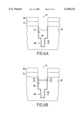
- FIG. 6A shows the spacer material filling portions of the trench region in accordance with the present invention
- FIG. 6B shows the spacer material filling portions of the trench region and an HDP oxide layer in accordance with the present invention.
- FIG. 7 is a flowchart showing steps of the present invention.
- FIG. 1 shows an initial semiconductor structure for forming a shallow trench isolation region in accordance with the present invention.
- a pad oxide layer 24 and a pad silicon nitride (SiN) layer 21 are formed on a silicon substrate 23 using conventional methods.
- a densified tetraethylorthosilicate (TEOS) layer 20 is formed optionally on the pad silicon nitride layer 21.
- This structure is covered with an insulating boron silicate glass (BSG) hardmask layer 22 before any active area lithography.
- BSG insulating boron silicate glass
- FIG. 2 shows a conventional photoresist 30 placed on the BSG hardmask layer 22.
- the photoresist 30 defines the active area and the isolation trench region 31 when the BSG hardmask layer 22, the TEOS layer 20 and the pad silicon nitride layer 21 are etched in a conventional manner.
- the trench region 31 is delineated by 1) applying a thin coat of the photoresist 30, 2) exposing selected regions of the photoresist 30 to light in order to induce a chemical change in the photoresist 30, and 3) removing the exposed portions of the photoresist 30 by wet-chemical means. Then the exposed regions are removed to a desired depth using an anisotropic subtractive etch process.
- RIE reactive ion etching
- plasma etching dry etching
- anisotropy anisotropy
- FIG. 3 shows the silicon substrate 23 etched to the requisite depth (preferably between 100 nm and 700 nm) and the BSG hardmask layer 22 stripped off the wafer using known etchants such as hydrofluoric (HF) vapor or HF/sulphuric wet etchant.
- etchants such as hydrofluoric (HF) vapor or HF/sulphuric wet etchant.
- Borophosphosilicate glass (BPSG) or other flowable glass such as PSG, BSG or ASG
- Plasma enhanced BPSG process allows for a thick planar film while allowing a thinner film on the sidewalls 41 of the trench region 31.
- the thinner film on the sidewalls 41 allows more space for etchants in subsequent steps.
- Doped glass may be flowed in a subsequent step. After the isolation etch and after the BSG hardmask layer 22 is stripped, the silicon may be nitridized with rapid thermal nitridation 29 (RTN) to prevent autodoping from the subsequent deposition of doped glass (e.g. BPSG).
- RTN rapid thermal nitridation 29
- FIG. 4 shows an embodiment in which the BPSG spacer material 50 is deposited by plasma-enhanced chemical vapor deposition (PECVD) prior to etching.
- PECVD plasma-enhanced chemical vapor deposition
- the BPSG spacer material 50 covers the sidewalls 41 and the bottom surface 42 of the trench region 31 as well as the top surface of the TEOS layer 20.
- FIG. 4 since there is a thicker BPSG layer on top of the structure, a deeper crevice may be etched in subsequent steps.
- the silicon substrate 23 is further etched preferably for an additional 50 nm to 500 nm to form a crevice region 60. Because of the width of the spacers 40 along the sidewalls 41, the width of the crevice region 60 is narrower than the width of the trench region 31 above the crevice region 60. This additional etching area of the crevice region 60 may continue as long as the pad nitride layer 21 is not exposed. This further etching allows for a significantly deeper isolation for vertical transistor isolation as in advanced DRAM cells. The deep isolation isolates different silicon islands. The larger silicon volume at the isolation bottom allows larger silicon volume for the buried strap depletion.
- FIG. 5 shows the etching of the silicon substrate 23 when the spacers 40 of the FIG. 3 embodiment are used, one skilled in the art would understand that similar etching into the silicon substrate 23 could also occur if the spacers 50 of the FIG. 4 embodiment were used. Deeper crevices may be etched in the FIG. 4 embodiment since the BPSG is thinner at the bottom during the spacer RIE step.
- a low temperature nitride (or oxide) layer 70 is grown along the exposed silicon surface 71 within the crevice region 60.
- the nitride layer 70 is grown preferably at a temperature less than about 700° C. in order to prevent any flow of the BPSG material forming the spacers 40.
- the nitride layer 70 is grown by rapid thermal nitridation (RTN) and is needed to prevent doping of the exposed silicon in the crevice region 60.
- FIG. 6A shows the reflowed BPSG material 72 within the trench region 31.
- the trench region 31 is subsequently filled (e.g., over the reflowed BPSG material 72) with conventional TEOS or HDP oxide.
- a thin HDP oxide layer 73 may be deposited as shown in FIG. 6B.
- the nitride layer 29 may be cleared out from the top of the trench region 31 with a wet etch and the silicon may be oxidized conventionally in area 74 so that the trench region 31 may be filled with TEOS or HDP oxide.
- FIG. 7 shows a flowchart showing steps of the present invention.
- the semiconductor substrate is formed preferably including a silicon substrate 23, a pad oxide layer 24, a pad silicon nitride layer 21, a TEOS layer 20 and a BSG layer 22.
- the trench region 31 is etched preferably using a photoresist 30.
- the BSG hardmask layer 22 is removed and in subsequent step S106, the BPSG material is deposited in the trench region 31 and is etched to form spacers 40/50 such as shown in FIGS. 3 or 4.
- spacers 40/50 such as shown in FIGS. 3 or 4.
- a nitridation of the silicon substrate 23 may be necessary before depositing spacers 40/50.
- step S108 the silicon substrate 23 is further etched to form a crevice region (or extended trench region) 60.
- step S110 a nitride layer 70 is grown along the exposed silicon surface substrate in the crevice region 60.
- step S112 the BPSG spacer material is flowed into the crevice region 60 preferably by heating the semiconductor structure at a high temperature.
- step S114 the trench region 31 is filled with an insulating material such as a high density plasma oxide or TEOS to complete the isolation separation of the trench region 31.
- the trench region 31 may be appropriately polished using chemical mechanical polishing as is well known to one skilled in the art. Using the above described steps, an isolation region is formed that extends deeper into the silicon substrate 23.
- isolation regions may be formed deeper than 7000 ⁇ . This is particularly important in advanced DRAM cells because of vertical gate transfer devices. Further, the BPSG material flows at a high temperature and acts like an oxide at a lower temperature. This makes it advantageous to be used as a spacer material during the etching process and as a filler material within the trench region following the formation of the crevice region 60. This also prevents gap fill problems in the deeper STI portions.
- the present invention is useful for isolation before deep trench silicon etches for capacitors in a DRAM.
- This invention is also useful for providing additional silicon deep in the substrate that can prevent pinch-off of the silicon from the buried strap of a vertical transistor.
- This invention also provides a method to fill an isolation region with doped glass without doping the silicon.
- the sidewalls of the trench region may be nitridized to form a nitride layer 29 prior to adding the spacer material 40/50.
- the spacer material 40/50 may be added to fill the trench region without forming a crevice region 60.
- an HDP oxide layer 73 may be added over the spacer material and the nitride layer above the HDP oxide layer 73 may be cleared out so that the silicon can be oxidized in area 74 and the trench region 31 can be filled with TEOS or HDP oxide.
Landscapes
- Element Separation (AREA)
Abstract
Description
Claims (29)
Priority Applications (1)
| Application Number | Priority Date | Filing Date | Title |
|---|---|---|---|
| US09/359,287 US6150212A (en) | 1999-07-22 | 1999-07-22 | Shallow trench isolation method utilizing combination of spacer and fill |
Applications Claiming Priority (1)
| Application Number | Priority Date | Filing Date | Title |
|---|---|---|---|
| US09/359,287 US6150212A (en) | 1999-07-22 | 1999-07-22 | Shallow trench isolation method utilizing combination of spacer and fill |
Publications (1)
| Publication Number | Publication Date |
|---|---|
| US6150212A true US6150212A (en) | 2000-11-21 |
Family
ID=23413167
Family Applications (1)
| Application Number | Title | Priority Date | Filing Date |
|---|---|---|---|
| US09/359,287 Expired - Fee Related US6150212A (en) | 1999-07-22 | 1999-07-22 | Shallow trench isolation method utilizing combination of spacer and fill |
Country Status (1)
| Country | Link |
|---|---|
| US (1) | US6150212A (en) |
Cited By (38)
| Publication number | Priority date | Publication date | Assignee | Title |
|---|---|---|---|---|
| US6261914B1 (en) * | 1999-07-27 | 2001-07-17 | International Business Machines Corporation | Process for improving local uniformity of chemical mechanical polishing using a self-aligned polish rate enhancement layer |
| US6294419B1 (en) * | 1999-04-30 | 2001-09-25 | International Business Machines Corporation | Structure and method for improved latch-up using dual depth STI with impurity implant |
| US6413835B1 (en) * | 1999-09-17 | 2002-07-02 | Telefonaktiebolaget Lm Ericsson (Publ) | Semiconductor structure and fabrication method of shallow and deep trenches |
| US6448149B1 (en) * | 1999-07-03 | 2002-09-10 | Samsung Electronics Co, Ltd. | Method for making shallow trench isolation in semiconductor fabrication |
| US20030017668A1 (en) * | 2001-07-20 | 2003-01-23 | Gerd Lichter | Method for fabricating self-aligning mask layers |
| US6518641B2 (en) | 2001-05-18 | 2003-02-11 | International Business Machines Corporation | Deep slit isolation with controlled void |
| US20030064598A1 (en) * | 2001-10-03 | 2003-04-03 | Promos Technologies, Inc. | Method of buried strap out-diffusion formation by gas phase doping |
| US6673696B1 (en) * | 2003-01-14 | 2004-01-06 | Advanced Micro Devices, Inc. | Post trench fill oxidation process for strained silicon processes |
| WO2003046977A3 (en) * | 2001-11-27 | 2004-02-12 | Austriamicrosystems Ag | Insulation trench for an integrated circuit and method for production thereof |
| US6740601B2 (en) | 2001-05-11 | 2004-05-25 | Applied Materials Inc. | HDP-CVD deposition process for filling high aspect ratio gaps |
| US20040137742A1 (en) * | 2003-01-14 | 2004-07-15 | Advanced Micro Devices, Inc. | Shallow trench isolation for strained silicon processes |
| US20040142964A1 (en) * | 1999-07-02 | 2004-07-22 | Smithkline Beecham P.L.C. | Novel compounds |
| US20040149388A1 (en) * | 2000-10-19 | 2004-08-05 | Klaus Breitschwerdt | Device and method for etching a substrate by using an inductively coupled plasma |
| US20040180509A1 (en) * | 2003-03-14 | 2004-09-16 | Advanced Micro Devices, Inc. | Shallow trench isolation for strained silicon processes |
| US20040180550A1 (en) * | 2003-03-12 | 2004-09-16 | Macronix International Co.,Ltd. | Method for forming shallow trench isolation with control of bird beak |
| US20040188385A1 (en) * | 2003-03-26 | 2004-09-30 | Kenji Yamada | Etching agent composition for thin films having high permittivity and process for etching |
| US6818528B2 (en) * | 2001-10-24 | 2004-11-16 | International Business Machines Corporation | Method for multi-depth trench isolation |
| US20050095807A1 (en) * | 2003-01-14 | 2005-05-05 | Advanced Micro Devices, Inc. | Silicon buffered shallow trench isolation for strained silicon processes |
| US20050151222A1 (en) * | 2004-01-12 | 2005-07-14 | Advanced Micro Devices, Inc. | Shallow trench isolation process and structure with minimized strained silicon consumption |
| US6921709B1 (en) | 2003-07-15 | 2005-07-26 | Advanced Micro Devices, Inc. | Front side seal to prevent germanium outgassing |
| US6962857B1 (en) | 2003-02-05 | 2005-11-08 | Advanced Micro Devices, Inc. | Shallow trench isolation process using oxide deposition and anneal |
| US20050260825A1 (en) * | 2003-02-25 | 2005-11-24 | International Business Machines Corporation | Shallow trench isolation structure for strained Si on SiGe |
| US7029987B2 (en) * | 2001-04-27 | 2006-04-18 | Samsung Electronics Co., Ltd. | Method of manufacturing semiconductor device having shallow trench isolation (STI) |
| US20060226559A1 (en) * | 2005-04-11 | 2006-10-12 | Texas Instruments Incorporated | Nitridation of sti liner oxide for modulating inverse width effects in semiconductor devices |
| US20060261436A1 (en) * | 2005-05-19 | 2006-11-23 | Freescale Semiconductor, Inc. | Electronic device including a trench field isolation region and a process for forming the same |
| CN1294639C (en) * | 2002-12-05 | 2007-01-10 | 台湾积体电路制造股份有限公司 | Manufacturing method of shallow trench and deep trench isolation structure |
| WO2007011566A1 (en) * | 2005-07-19 | 2007-01-25 | Micron Technology, Inc. | Semiconductor constructions, memory arrays, electronic systems, and methods of forming semiconductor constructions |
| US20070045769A1 (en) * | 2005-09-01 | 2007-03-01 | Micron Technology, Inc. | Semiconductor constructions, memory arrays, electronic systems, and methods of forming semiconductor constructions |
| US20070212848A1 (en) * | 2006-03-10 | 2007-09-13 | Micron Technology, Inc. | Method of making an isolation trench and resulting isolation trench |
| US20070212874A1 (en) * | 2006-03-08 | 2007-09-13 | Micron Technology, Inc. | Method for filling shallow isolation trenches and other recesses during the formation of a semiconductor device and electronic systems including the semiconductor device |
| US20070238295A1 (en) * | 2006-04-11 | 2007-10-11 | Micron Technology, Inc. | Methods of forming semiconductor constructions |
| US7491622B2 (en) | 2006-04-24 | 2009-02-17 | Freescale Semiconductor, Inc. | Process of forming an electronic device including a layer formed using an inductively coupled plasma |
| US7528078B2 (en) | 2006-05-12 | 2009-05-05 | Freescale Semiconductor, Inc. | Process of forming electronic device including a densified nitride layer adjacent to an opening within a semiconductor layer |
| US7670895B2 (en) | 2006-04-24 | 2010-03-02 | Freescale Semiconductor, Inc | Process of forming an electronic device including a semiconductor layer and another layer adjacent to an opening within the semiconductor layer |
| CN103000512A (en) * | 2011-09-13 | 2013-03-27 | 联华电子股份有限公司 | Method for patterning hard mask layers for defining deep trenches |
| US20130093062A1 (en) * | 2011-10-18 | 2013-04-18 | Ying-Chih Lin | Semiconductor structure and process thereof |
| US20140159193A1 (en) * | 2012-12-11 | 2014-06-12 | SK Hynix Inc. | Semiconductor device and method for fabricating the same |
| US20150170972A1 (en) * | 2013-12-12 | 2015-06-18 | Texas Instruments Incorporated | Method to form silicide and contact at embedded epitaxial facet |
Citations (4)
| Publication number | Priority date | Publication date | Assignee | Title |
|---|---|---|---|---|
| US5895253A (en) * | 1997-08-22 | 1999-04-20 | Micron Technology, Inc. | Trench isolation for CMOS devices |
| US5939333A (en) * | 1996-05-30 | 1999-08-17 | Micron Technology, Inc. | Silicon nitride deposition method |
| US5945704A (en) * | 1998-04-06 | 1999-08-31 | Siemens Aktiengesellschaft | Trench capacitor with epi buried layer |
| US5994209A (en) * | 1996-11-13 | 1999-11-30 | Applied Materials, Inc. | Methods and apparatus for forming ultra-shallow doped regions using doped silicon oxide films |
-
1999
- 1999-07-22 US US09/359,287 patent/US6150212A/en not_active Expired - Fee Related
Patent Citations (4)
| Publication number | Priority date | Publication date | Assignee | Title |
|---|---|---|---|---|
| US5939333A (en) * | 1996-05-30 | 1999-08-17 | Micron Technology, Inc. | Silicon nitride deposition method |
| US5994209A (en) * | 1996-11-13 | 1999-11-30 | Applied Materials, Inc. | Methods and apparatus for forming ultra-shallow doped regions using doped silicon oxide films |
| US5895253A (en) * | 1997-08-22 | 1999-04-20 | Micron Technology, Inc. | Trench isolation for CMOS devices |
| US5945704A (en) * | 1998-04-06 | 1999-08-31 | Siemens Aktiengesellschaft | Trench capacitor with epi buried layer |
Cited By (75)
| Publication number | Priority date | Publication date | Assignee | Title |
|---|---|---|---|---|
| US6294419B1 (en) * | 1999-04-30 | 2001-09-25 | International Business Machines Corporation | Structure and method for improved latch-up using dual depth STI with impurity implant |
| US20040142964A1 (en) * | 1999-07-02 | 2004-07-22 | Smithkline Beecham P.L.C. | Novel compounds |
| US7105536B2 (en) | 1999-07-02 | 2006-09-12 | Smithkline Beecham Plc | Compounds |
| US6448149B1 (en) * | 1999-07-03 | 2002-09-10 | Samsung Electronics Co, Ltd. | Method for making shallow trench isolation in semiconductor fabrication |
| US6261914B1 (en) * | 1999-07-27 | 2001-07-17 | International Business Machines Corporation | Process for improving local uniformity of chemical mechanical polishing using a self-aligned polish rate enhancement layer |
| US6413835B1 (en) * | 1999-09-17 | 2002-07-02 | Telefonaktiebolaget Lm Ericsson (Publ) | Semiconductor structure and fabrication method of shallow and deep trenches |
| US20040149388A1 (en) * | 2000-10-19 | 2004-08-05 | Klaus Breitschwerdt | Device and method for etching a substrate by using an inductively coupled plasma |
| US7029987B2 (en) * | 2001-04-27 | 2006-04-18 | Samsung Electronics Co., Ltd. | Method of manufacturing semiconductor device having shallow trench isolation (STI) |
| US6914016B2 (en) | 2001-05-11 | 2005-07-05 | Applied Materials, Inc. | HDP-CVD deposition process for filling high aspect ratio gaps |
| US6740601B2 (en) | 2001-05-11 | 2004-05-25 | Applied Materials Inc. | HDP-CVD deposition process for filling high aspect ratio gaps |
| US7196021B2 (en) | 2001-05-11 | 2007-03-27 | Applied Materials, Inc. | HDP-CVD deposition process for filling high aspect ratio gaps |
| US6518641B2 (en) | 2001-05-18 | 2003-02-11 | International Business Machines Corporation | Deep slit isolation with controlled void |
| US20030017668A1 (en) * | 2001-07-20 | 2003-01-23 | Gerd Lichter | Method for fabricating self-aligning mask layers |
| US6794259B2 (en) * | 2001-07-20 | 2004-09-21 | Infineon Technologies Ag | Method for fabricating self-aligning mask layers |
| US6734106B2 (en) * | 2001-10-03 | 2004-05-11 | Promos Technologies, Inc. | Method of buried strap out-diffusion formation by gas phase doping |
| US20030064598A1 (en) * | 2001-10-03 | 2003-04-03 | Promos Technologies, Inc. | Method of buried strap out-diffusion formation by gas phase doping |
| US6818528B2 (en) * | 2001-10-24 | 2004-11-16 | International Business Machines Corporation | Method for multi-depth trench isolation |
| WO2003046977A3 (en) * | 2001-11-27 | 2004-02-12 | Austriamicrosystems Ag | Insulation trench for an integrated circuit and method for production thereof |
| CN1294639C (en) * | 2002-12-05 | 2007-01-10 | 台湾积体电路制造股份有限公司 | Manufacturing method of shallow trench and deep trench isolation structure |
| US7238588B2 (en) | 2003-01-14 | 2007-07-03 | Advanced Micro Devices, Inc. | Silicon buffered shallow trench isolation |
| US20050095807A1 (en) * | 2003-01-14 | 2005-05-05 | Advanced Micro Devices, Inc. | Silicon buffered shallow trench isolation for strained silicon processes |
| US7648886B2 (en) | 2003-01-14 | 2010-01-19 | Globalfoundries Inc. | Shallow trench isolation process |
| US6673696B1 (en) * | 2003-01-14 | 2004-01-06 | Advanced Micro Devices, Inc. | Post trench fill oxidation process for strained silicon processes |
| US20040137742A1 (en) * | 2003-01-14 | 2004-07-15 | Advanced Micro Devices, Inc. | Shallow trench isolation for strained silicon processes |
| US6962857B1 (en) | 2003-02-05 | 2005-11-08 | Advanced Micro Devices, Inc. | Shallow trench isolation process using oxide deposition and anneal |
| US20050260825A1 (en) * | 2003-02-25 | 2005-11-24 | International Business Machines Corporation | Shallow trench isolation structure for strained Si on SiGe |
| US7183175B2 (en) | 2003-02-25 | 2007-02-27 | International Business Machines Corporation | Shallow trench isolation structure for strained Si on SiGe |
| US6984553B2 (en) * | 2003-03-12 | 2006-01-10 | Macronix International Co., Ltd. | Method for forming shallow trench isolation with control of bird beak |
| US20040180550A1 (en) * | 2003-03-12 | 2004-09-16 | Macronix International Co.,Ltd. | Method for forming shallow trench isolation with control of bird beak |
| US7713834B2 (en) | 2003-03-14 | 2010-05-11 | Globalfoundries Inc. | Method of forming isolation regions for integrated circuits |
| US7422961B2 (en) | 2003-03-14 | 2008-09-09 | Advanced Micro Devices, Inc. | Method of forming isolation regions for integrated circuits |
| US20040180509A1 (en) * | 2003-03-14 | 2004-09-16 | Advanced Micro Devices, Inc. | Shallow trench isolation for strained silicon processes |
| US20090047770A1 (en) * | 2003-03-14 | 2009-02-19 | Advanced Micro Devices, Inc. | Method of forming isolation regions for integrated circuits |
| US20040188385A1 (en) * | 2003-03-26 | 2004-09-30 | Kenji Yamada | Etching agent composition for thin films having high permittivity and process for etching |
| US6921709B1 (en) | 2003-07-15 | 2005-07-26 | Advanced Micro Devices, Inc. | Front side seal to prevent germanium outgassing |
| US20080213952A1 (en) * | 2004-01-12 | 2008-09-04 | Advanced Micro Devices, Inc. | Shallow trench isolation process and structure with minimized strained silicon consumption |
| US20050151222A1 (en) * | 2004-01-12 | 2005-07-14 | Advanced Micro Devices, Inc. | Shallow trench isolation process and structure with minimized strained silicon consumption |
| US7732336B2 (en) | 2004-01-12 | 2010-06-08 | Globalfoundries Inc. | Shallow trench isolation process and structure with minimized strained silicon consumption |
| US7462549B2 (en) | 2004-01-12 | 2008-12-09 | Advanced Micro Devices, Inc. | Shallow trench isolation process and structure with minimized strained silicon consumption |
| US7199020B2 (en) * | 2005-04-11 | 2007-04-03 | Texas Instruments Incorporated | Nitridation of STI liner oxide for modulating inverse width effects in semiconductor devices |
| US20060226559A1 (en) * | 2005-04-11 | 2006-10-12 | Texas Instruments Incorporated | Nitridation of sti liner oxide for modulating inverse width effects in semiconductor devices |
| US20060261436A1 (en) * | 2005-05-19 | 2006-11-23 | Freescale Semiconductor, Inc. | Electronic device including a trench field isolation region and a process for forming the same |
| US20070018215A1 (en) * | 2005-07-19 | 2007-01-25 | Micron Technology, Inc. | Semiconductor constructions, memory arrays, electronic systems, and methods of forming semiconductor constructions |
| US20070235783A9 (en) * | 2005-07-19 | 2007-10-11 | Micron Technology, Inc. | Semiconductor constructions, memory arrays, electronic systems, and methods of forming semiconductor constructions |
| WO2007011566A1 (en) * | 2005-07-19 | 2007-01-25 | Micron Technology, Inc. | Semiconductor constructions, memory arrays, electronic systems, and methods of forming semiconductor constructions |
| US10622442B2 (en) | 2005-09-01 | 2020-04-14 | Micron Technology, Inc. | Electronic systems and methods of forming semiconductor constructions |
| US8829643B2 (en) | 2005-09-01 | 2014-09-09 | Micron Technology, Inc. | Memory arrays |
| US9929233B2 (en) | 2005-09-01 | 2018-03-27 | Micron Technology, Inc. | Memory arrays |
| US11626481B2 (en) | 2005-09-01 | 2023-04-11 | Micron Technology, Inc. | Semiconductor constructions, memory arrays, electronic systems, and methods of forming semiconductor constructions |
| US11171205B2 (en) | 2005-09-01 | 2021-11-09 | Micron Technology, Inc. | Semiconductor constructions, memory arrays, electronic systems, and methods of forming semiconductor constructions |
| US10170545B2 (en) | 2005-09-01 | 2019-01-01 | Micron Technology, Inc. | Memory arrays |
| US9559163B2 (en) | 2005-09-01 | 2017-01-31 | Micron Technology, Inc. | Memory arrays |
| US20070045769A1 (en) * | 2005-09-01 | 2007-03-01 | Micron Technology, Inc. | Semiconductor constructions, memory arrays, electronic systems, and methods of forming semiconductor constructions |
| US7772672B2 (en) | 2005-09-01 | 2010-08-10 | Micron Technology, Inc. | Semiconductor constructions |
| US20070212874A1 (en) * | 2006-03-08 | 2007-09-13 | Micron Technology, Inc. | Method for filling shallow isolation trenches and other recesses during the formation of a semiconductor device and electronic systems including the semiconductor device |
| US7375004B2 (en) * | 2006-03-10 | 2008-05-20 | Micron Technology, Inc. | Method of making an isolation trench and resulting isolation trench |
| US7999328B2 (en) * | 2006-03-10 | 2011-08-16 | Micron Technology, Inc. | Isolation trench having first and second trench areas of different widths |
| US20070212848A1 (en) * | 2006-03-10 | 2007-09-13 | Micron Technology, Inc. | Method of making an isolation trench and resulting isolation trench |
| US20070210390A1 (en) * | 2006-03-10 | 2007-09-13 | Sukesh Sandhu | Method of making an isolation trench and resulting isolation trench |
| US7799694B2 (en) | 2006-04-11 | 2010-09-21 | Micron Technology, Inc. | Methods of forming semiconductor constructions |
| US8598043B2 (en) | 2006-04-11 | 2013-12-03 | Micron Technology Inc. | Methods of forming semiconductor constructions |
| US20070238295A1 (en) * | 2006-04-11 | 2007-10-11 | Micron Technology, Inc. | Methods of forming semiconductor constructions |
| US7670895B2 (en) | 2006-04-24 | 2010-03-02 | Freescale Semiconductor, Inc | Process of forming an electronic device including a semiconductor layer and another layer adjacent to an opening within the semiconductor layer |
| US7491622B2 (en) | 2006-04-24 | 2009-02-17 | Freescale Semiconductor, Inc. | Process of forming an electronic device including a layer formed using an inductively coupled plasma |
| US7528078B2 (en) | 2006-05-12 | 2009-05-05 | Freescale Semiconductor, Inc. | Process of forming electronic device including a densified nitride layer adjacent to an opening within a semiconductor layer |
| CN103000512B (en) * | 2011-09-13 | 2017-08-22 | 联华电子股份有限公司 | Method for patterning hard mask layer for defining deep trench |
| CN103000512A (en) * | 2011-09-13 | 2013-03-27 | 联华电子股份有限公司 | Method for patterning hard mask layers for defining deep trenches |
| US9013024B2 (en) | 2011-10-18 | 2015-04-21 | United Microelectronics Corp. | Semiconductor structure and process thereof |
| US20130093062A1 (en) * | 2011-10-18 | 2013-04-18 | Ying-Chih Lin | Semiconductor structure and process thereof |
| US8994144B2 (en) * | 2012-12-11 | 2015-03-31 | SK Hynix Inc. | Semiconductor device and method for fabricating the same |
| US20140159193A1 (en) * | 2012-12-11 | 2014-06-12 | SK Hynix Inc. | Semiconductor device and method for fabricating the same |
| US20150170972A1 (en) * | 2013-12-12 | 2015-06-18 | Texas Instruments Incorporated | Method to form silicide and contact at embedded epitaxial facet |
| US9508601B2 (en) * | 2013-12-12 | 2016-11-29 | Texas Instruments Incorporated | Method to form silicide and contact at embedded epitaxial facet |
| US9812452B2 (en) | 2013-12-12 | 2017-11-07 | Texas Instruments Incorporated | Method to form silicide and contact at embedded epitaxial facet |
| US10008499B2 (en) | 2013-12-12 | 2018-06-26 | Texas Instruments Incorporated | Method to form silicide and contact at embedded epitaxial facet |
Similar Documents
| Publication | Publication Date | Title |
|---|---|---|
| US6150212A (en) | Shallow trench isolation method utilizing combination of spacer and fill | |
| US6214696B1 (en) | Method of fabricating deep-shallow trench isolation | |
| US5313094A (en) | Thermal dissipation of integrated circuits using diamond paths | |
| US6137152A (en) | Planarized deep-shallow trench isolation for CMOS/bipolar devices | |
| US6265302B1 (en) | Partially recessed shallow trench isolation method for fabricating borderless contacts | |
| US5801082A (en) | Method for making improved shallow trench isolation with dielectric studs for semiconductor integrated circuits | |
| US6020230A (en) | Process to fabricate planarized deep-shallow trench isolation having upper and lower portions with oxidized semiconductor trench fill in the upper portion and semiconductor trench fill in the lower portion | |
| KR100193976B1 (en) | Semiconductor Trench Capacitor Cell with Buried Strap | |
| US8039326B2 (en) | Methods for fabricating bulk FinFET devices having deep trench isolation | |
| US6297126B1 (en) | Silicon nitride capped shallow trench isolation method for fabricating sub-micron devices with borderless contacts | |
| US6649959B2 (en) | Method for increasing a very-large-scale-integrated (VLSI) capacitor size on bulk silicon and silicon-on-insulator (SOI) wafers and structure formed thereby | |
| US6008084A (en) | Method for fabricating low resistance bit line structures, along with bit line structures exhibiting low bit line to bit line coupling capacitance | |
| US6232202B1 (en) | Method for manufacturing shallow trench isolation structure including a dual trench | |
| US6194283B1 (en) | High density trench fill due to new spacer fill method including isotropically etching silicon nitride spacers | |
| US6114219A (en) | Method of manufacturing an isolation region in a semiconductor device using a flowable oxide-generating material | |
| KR100193975B1 (en) | Semiconductor Trench Capacitor Cell with Buried Strap | |
| US6180493B1 (en) | Method for forming shallow trench isolation region | |
| US10903207B2 (en) | Method of forming an integrated circuit (IC) with shallow trench isolation (STI) regions and the resulting IC structure | |
| US6063657A (en) | Method of forming a buried strap in a DRAM | |
| US20010006839A1 (en) | Method for manufacturing shallow trench isolation in semiconductor device | |
| US6297127B1 (en) | Self-aligned deep trench isolation to shallow trench isolation | |
| US6551901B1 (en) | Method for preventing borderless contact to well leakage | |
| KR100251280B1 (en) | Sti method | |
| US6884714B2 (en) | Method of forming shallow trench isolation with chamfered corners | |
| US5923991A (en) | Methods to prevent divot formation in shallow trench isolation areas |
Legal Events
| Date | Code | Title | Description |
|---|---|---|---|
| AS | Assignment |
Owner name: INTERNATIONAL BUSINESS MACHINES CORPORATION, NEW Y Free format text: ASSIGNMENT OF ASSIGNORS INTEREST;ASSIGNORS:DIVAKARUNI, RAMACHANDRA;GAMBINO, JEFFREY P.;MANDELMAN, JACK A.;AND OTHERS;REEL/FRAME:010123/0595;SIGNING DATES FROM 19990707 TO 19990719 |
|
| FEPP | Fee payment procedure |
Free format text: PAYOR NUMBER ASSIGNED (ORIGINAL EVENT CODE: ASPN); ENTITY STATUS OF PATENT OWNER: LARGE ENTITY |
|
| FEPP | Fee payment procedure |
Free format text: PAYER NUMBER DE-ASSIGNED (ORIGINAL EVENT CODE: RMPN); ENTITY STATUS OF PATENT OWNER: LARGE ENTITY Free format text: PAYOR NUMBER ASSIGNED (ORIGINAL EVENT CODE: ASPN); ENTITY STATUS OF PATENT OWNER: LARGE ENTITY |
|
| FEPP | Fee payment procedure |
Free format text: PAYER NUMBER DE-ASSIGNED (ORIGINAL EVENT CODE: RMPN); ENTITY STATUS OF PATENT OWNER: LARGE ENTITY Free format text: PAYOR NUMBER ASSIGNED (ORIGINAL EVENT CODE: ASPN); ENTITY STATUS OF PATENT OWNER: LARGE ENTITY |
|
| FPAY | Fee payment |
Year of fee payment: 4 |
|
| REMI | Maintenance fee reminder mailed | ||
| LAPS | Lapse for failure to pay maintenance fees | ||
| LAPS | Lapse for failure to pay maintenance fees |
Free format text: PATENT EXPIRED FOR FAILURE TO PAY MAINTENANCE FEES (ORIGINAL EVENT CODE: EXP.); ENTITY STATUS OF PATENT OWNER: LARGE ENTITY |
|
| STCH | Information on status: patent discontinuation |
Free format text: PATENT EXPIRED DUE TO NONPAYMENT OF MAINTENANCE FEES UNDER 37 CFR 1.362 |
|
| FP | Lapsed due to failure to pay maintenance fee |
Effective date: 20081121 |