US6150205A - Method of fabricating dual gate - Google Patents
Method of fabricating dual gate Download PDFInfo
- Publication number
- US6150205A US6150205A US09/227,761 US22776199A US6150205A US 6150205 A US6150205 A US 6150205A US 22776199 A US22776199 A US 22776199A US 6150205 A US6150205 A US 6150205A
- Authority
- US
- United States
- Prior art keywords
- layer
- conductive
- ions
- conductive type
- thermal process
- Prior art date
- Legal status (The legal status is an assumption and is not a legal conclusion. Google has not performed a legal analysis and makes no representation as to the accuracy of the status listed.)
- Expired - Lifetime
Links
- 230000009977 dual effect Effects 0.000 title claims abstract description 16
- 238000004519 manufacturing process Methods 0.000 title claims abstract description 15
- 238000000034 method Methods 0.000 claims abstract description 66
- 229910021420 polycrystalline silicon Inorganic materials 0.000 claims abstract description 62
- 229920005591 polysilicon Polymers 0.000 claims abstract description 62
- 229910052751 metal Inorganic materials 0.000 claims abstract description 30
- 239000002184 metal Substances 0.000 claims abstract description 30
- 238000009792 diffusion process Methods 0.000 claims abstract description 27
- 150000002500 ions Chemical class 0.000 claims abstract description 25
- 229910021332 silicide Inorganic materials 0.000 claims abstract description 23
- FVBUAEGBCNSCDD-UHFFFAOYSA-N silicide(4-) Chemical compound [Si-4] FVBUAEGBCNSCDD-UHFFFAOYSA-N 0.000 claims abstract description 23
- 238000002955 isolation Methods 0.000 claims abstract description 8
- 239000000758 substrate Substances 0.000 claims description 13
- XUIMIQQOPSSXEZ-UHFFFAOYSA-N Silicon Chemical compound [Si] XUIMIQQOPSSXEZ-UHFFFAOYSA-N 0.000 claims description 10
- 229910052710 silicon Inorganic materials 0.000 claims description 10
- 239000010703 silicon Substances 0.000 claims description 10
- 238000005468 ion implantation Methods 0.000 claims description 7
- 229910052796 boron Inorganic materials 0.000 claims description 4
- 238000006243 chemical reaction Methods 0.000 claims description 4
- -1 boron ions Chemical class 0.000 claims description 3
- 238000000137 annealing Methods 0.000 claims 2
- 238000000059 patterning Methods 0.000 claims 2
- 230000001939 inductive effect Effects 0.000 claims 1
- 230000001131 transforming effect Effects 0.000 claims 1
- 229910021341 titanium silicide Inorganic materials 0.000 description 5
- 229910052581 Si3N4 Inorganic materials 0.000 description 4
- 239000004065 semiconductor Substances 0.000 description 4
- HQVNEWCFYHHQES-UHFFFAOYSA-N silicon nitride Chemical compound N12[Si]34N5[Si]62N3[Si]51N64 HQVNEWCFYHHQES-UHFFFAOYSA-N 0.000 description 4
- 238000004518 low pressure chemical vapour deposition Methods 0.000 description 3
- 238000007796 conventional method Methods 0.000 description 2
- 230000000694 effects Effects 0.000 description 2
- 229910044991 metal oxide Inorganic materials 0.000 description 2
- 150000004706 metal oxides Chemical class 0.000 description 2
- 238000000206 photolithography Methods 0.000 description 2
- ZOXJGFHDIHLPTG-UHFFFAOYSA-N Boron Chemical compound [B] ZOXJGFHDIHLPTG-UHFFFAOYSA-N 0.000 description 1
- RTAQQCXQSZGOHL-UHFFFAOYSA-N Titanium Chemical compound [Ti] RTAQQCXQSZGOHL-UHFFFAOYSA-N 0.000 description 1
- 230000015572 biosynthetic process Effects 0.000 description 1
- 230000000295 complement effect Effects 0.000 description 1
- 238000009826 distribution Methods 0.000 description 1
- 238000001312 dry etching Methods 0.000 description 1
- 238000005530 etching Methods 0.000 description 1
- 239000000463 material Substances 0.000 description 1
- 230000003647 oxidation Effects 0.000 description 1
- 238000007254 oxidation reaction Methods 0.000 description 1
- 238000001020 plasma etching Methods 0.000 description 1
- 238000004544 sputter deposition Methods 0.000 description 1
- 239000010936 titanium Substances 0.000 description 1
- 229910052719 titanium Inorganic materials 0.000 description 1
- WQJQOUPTWCFRMM-UHFFFAOYSA-N tungsten disilicide Chemical compound [Si]#[W]#[Si] WQJQOUPTWCFRMM-UHFFFAOYSA-N 0.000 description 1
- 229910021342 tungsten silicide Inorganic materials 0.000 description 1
- 230000005641 tunneling Effects 0.000 description 1
Images

Classifications
-
- H—ELECTRICITY
- H10—SEMICONDUCTOR DEVICES; ELECTRIC SOLID-STATE DEVICES NOT OTHERWISE PROVIDED FOR
- H10D—INORGANIC ELECTRIC SEMICONDUCTOR DEVICES
- H10D84/00—Integrated devices formed in or on semiconductor substrates that comprise only semiconducting layers, e.g. on Si wafers or on GaAs-on-Si wafers
- H10D84/01—Manufacture or treatment
- H10D84/0123—Integrating together multiple components covered by H10D12/00 or H10D30/00, e.g. integrating multiple IGBTs
- H10D84/0126—Integrating together multiple components covered by H10D12/00 or H10D30/00, e.g. integrating multiple IGBTs the components including insulated gates, e.g. IGFETs
- H10D84/0165—Integrating together multiple components covered by H10D12/00 or H10D30/00, e.g. integrating multiple IGBTs the components including insulated gates, e.g. IGFETs the components including complementary IGFETs, e.g. CMOS devices
- H10D84/0172—Manufacturing their gate conductors
- H10D84/0177—Manufacturing their gate conductors the gate conductors having different materials or different implants
-
- H—ELECTRICITY
- H10—SEMICONDUCTOR DEVICES; ELECTRIC SOLID-STATE DEVICES NOT OTHERWISE PROVIDED FOR
- H10D—INORGANIC ELECTRIC SEMICONDUCTOR DEVICES
- H10D84/00—Integrated devices formed in or on semiconductor substrates that comprise only semiconducting layers, e.g. on Si wafers or on GaAs-on-Si wafers
- H10D84/01—Manufacture or treatment
- H10D84/02—Manufacture or treatment characterised by using material-based technologies
- H10D84/03—Manufacture or treatment characterised by using material-based technologies using Group IV technology, e.g. silicon technology or silicon-carbide [SiC] technology
- H10D84/038—Manufacture or treatment characterised by using material-based technologies using Group IV technology, e.g. silicon technology or silicon-carbide [SiC] technology using silicon technology, e.g. SiGe
Definitions
- the invention relates to a method of fabricating a gate of a semiconductor device, and more particularly, to a method of forming a dual gate.
- a gate has to be formed with a smaller and smaller dimension, and with a faster and faster operation speed.
- the operation voltage is thus lowered, and consequently, to demand a change in material and fabrication to avoid any device instability.
- NMOS N-channel metal-oxide semiconductor
- PMOS P-channel metal-oxide semiconductor
- a gate is formed of a polysilicon layer doped with N-type ions.
- a tungsten silicide layer and a silicon nitride layer are then formed on the gate.
- an ion implantation is performed to an N-well or an N-type substrate for adjusting the threshold voltage of the PMOS.
- a PN junction is formed to induce a depletion region.
- the induced depletion region induces an equivalent buried channel device to cause a short channel effect, so that problems Such as sub-threshold voltage and out-of-control of the device by its gate.
- CMOS complementary MOS
- Embedded DRAM embedded dynamic random access memory
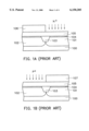
- FIG. 1A to FIG. 1D show a conventional method of fabricating a dual gate.
- a substrate 100 is provided.
- an N-well 101 and a P-well 102 are formed in the substrate 100.
- a shallow trench isolation 103 is formed between the N-well 101 and P-well 102 for isolation.
- a gate oxide layer 104 is formed on the substrate 100.
- a polysilicon layer 105 is formed on the gate oxide layer 104.
- the part of the polysilicon layer 105 over the P-well 102 is covered by a photo-resist layer 106, while the other part polysilicon layer 105 over the N-well 101 is exposed.
- N-type ions are implanted to the exposed part of the polysilicon layer 105.
- the photo-resist layer 106 is removed.
- Another photo-resist layer 107 is formed to cover the part of the polysilicon layer 105 over the N-well 101, and the polysilicon layer 105 over the P-well 102 is exposed. P-type ions are implanted into the P-well 102.
- the photo-resist layer 107 is removed.
- a high temperature diffusion is performed to define the N-type polysilicon layer 105a on the N-well and the P-type polysilicon layer 105b on the P-well 105b.
- a titanium silicide layer 108 is formed on the N-type polysilicon layer 105a and the P-type polysilicon layer 105b.
- a silicon nitride layer 109 is formed on the titanium silicide layer 108.
- the silicon nitride layer 109, the titanium silicide layer 108, the polysilicon layers 105a and 105b are patterned to form a gate on the N-well 101 and a gate on the P-well 102.
- the polysilicon layer has to be doped by two ion implantation steps with the aid of forming two photo-resist layers by two photolithography processes.
- the fabrication process is complex, so that a long process time is consumed.
- two photo-resist layers are formed, so that the fabrication cost is high.
- a method of fabricating a dual gate is provided.
- a first conductive type region and a second conductive type region isolated by an isolation structure are provided.
- a polysilicon layer is formed to comprise a first part covering the first conductive type region and a second part covering the second conductive type region.
- the first part of the polysilicon layer is converted into a first conductive type polysilicon layer.
- a diffusion layer containing second type conductive ions is formed to cover the first part of the polysilicon layer.
- a first thermal process is performed to convert the second part of the polysilicon layer into a second conductive type polysilicon layer.
- a metal layer is formed on the diffusion layer and the first conductive type polysilicon layer.
- the metal layer is transformed into a metal silicide layer, and simultaneously, a reaction is induced between the metal layer and the diffusion layer.
- a dielectric layer is formed on the metal silicide layer.
- the dielectric layer, the metal silicide layer, the reacted diffusion layer, the first and the second conductive type polysilicon layers are patterned to form a first conductive type gate on the first conductive region and a second conductive type gate on the second conductive type region.
- FIG. 1A to FIG. 1D are cross sectional views showing a conventional method for fabricating a dual gate
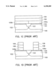
- FIG. 2A to FIG. 2E are cross sectional views showing a method for fabricating a dual gate in a preferred embodiment according to invention.
- a substrate 200 is provided.
- the substrate 200 comprises an N-well 201 and a P-well 202 isolated by an isolation structure, for example, a field oxide layer or a shallow trench isolation.
- the substrate 200 may also be replaced by an N-type substrate comprising a single P-type well, or a P-type substrate comprising a single N-well.
- a gate oxide layer 204 is formed, for example, by thermal oxidation, on the N-well 201 and the P-well 202.
- a polysilicon layer 205 is formed, for example, by low pressure chemical vapor deposition (LPCVD) on the gate oxide layer 204.
- a diffusion layer 206 is formed to cover the P-type polysilicon layer.
- the diffusion layer includes a silicon layer 206 containing P-type conductive ions, preferably, a P-type conductive-ions-containing polysilicon layer.
- the conductive-ions-containing silicon layer 206 is preferably formed by ultra high vacuum (UHV) CVD to a thickness of about 50 to 200 ⁇ .
- the conductive ions include P-type ions such as boron ions with a concentration of about 10 20 to 10 22 per unit cubic centimeter.
- the method for forming the conductive-ions-containing silicon layer 206 is referred as a source diffusion method and is introduced in more details in the U.S. Pat. No. 5,674,777.
- a photo-resist layer 207 is defined to cover a part of the conductive-ions-containing silicon layer 206 over the P-well 202, while the other part of the conductive-ions-containing silicon layer 206 over the N-well 201 is exposed.
- the exposed part of the conductive-ions-containing silicon layer 206 is removed, for example, by dry etchings so that the polysilicon layer 205 over the N-well 201 is exposed.
- the remaining, conductive ions contained silicon layer is denoted as 206a.
- an N-type ion implantation is performed to transform the exposed polysilicon layer 205 into an N-type polysilicon layer 205a.
- the photo-resist layer 207 is removed, for example, by plasma etching.
- a thermal process for example. a thermal anneal or a rapid thermal process at a temperature of about 700° C. to 900° C.
- the P-type conductive ions contained in the conductive-ions-containing polysilicon layer 206a diffuse into the polysilicon layer 205 over the P-well 102, so that the polysilicon layer 205 is transformed into a P-type polysilicon layer 205b.
- the N-type ions in the N-type polysilicon layer 205a call also be diffused further and evenly distributed.
- a metal silicide layer 208 for example, a titanium silicide layer or a titanium silicide/titanium layer, formed by sputtering is formed on the N-type polysilicon layer 205a and the conductive ions contained polysilicon layer 206a.
- a dielectric layer 209 for example, a silicon nitride layer formed by LPCVD, is formed on the metal silicide layer 208.
- a thermal process for example, a rapid thermal process is performed to cause a reaction between the metal silicide layer 208 and the conductive-ions-containing silicon layer 206a. After the reaction, the conductive-ions-containing silicon layer 205a is transformed into a conductive-ions-containing, silicide layer 206'.
- the dielectric layer 209, the metal silicide layer 208, the conductive-ions-containing silicide layer 206a, the N-type polysilicon layer 205a and the P-type polysilicon layer 205b are defined to form a dual gate structure.
- the dual gate structure comprises a gate on the N-well 201 and the other gate on the P-well 202.
- the gate on the N-well 201 further comprises the patterned N-type polysilicon layer 205a, the patterned metal silicide layer 208, and the patterned dielectric layer 209.
- the gate on the P-well further comprises the patterned P-type polysilicon layer 205b.
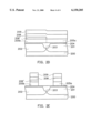
- an additional diffusion layer is formed to over the P-well.
- a thermal process is performed, so that the conductive ions contained in the diffusion layer are diffused into all underlying polysilicon layer to form a P-type polysilicon layer.
- the N-type ions implanted into the N-type polysilicon layer may further diffuse to obtain an more evenly distribution.
- a dual gate is thus formed with only one step of ion implantation.
- the invention also has an advantage of preventing problems caused by tunneling effect of implanted P-type (boron) ions to enhance the reliability of devices.
- the invention provides a gate with a reduced resistance by the formation of the conductive-ions-containing silicide layer.
- the gate is formed with a taster operation speed.
Landscapes
- Metal-Oxide And Bipolar Metal-Oxide Semiconductor Integrated Circuits (AREA)
- Electrodes Of Semiconductors (AREA)
Abstract
Description
Claims (28)
Priority Applications (1)
| Application Number | Priority Date | Filing Date | Title |
|---|---|---|---|
| US09/227,761 US6150205A (en) | 1999-01-08 | 1999-01-08 | Method of fabricating dual gate |
Applications Claiming Priority (1)
| Application Number | Priority Date | Filing Date | Title |
|---|---|---|---|
| US09/227,761 US6150205A (en) | 1999-01-08 | 1999-01-08 | Method of fabricating dual gate |
Publications (1)
| Publication Number | Publication Date |
|---|---|
| US6150205A true US6150205A (en) | 2000-11-21 |
Family
ID=22854353
Family Applications (1)
| Application Number | Title | Priority Date | Filing Date |
|---|---|---|---|
| US09/227,761 Expired - Lifetime US6150205A (en) | 1999-01-08 | 1999-01-08 | Method of fabricating dual gate |
Country Status (1)
| Country | Link |
|---|---|
| US (1) | US6150205A (en) |
Cited By (4)
| Publication number | Priority date | Publication date | Assignee | Title |
|---|---|---|---|---|
| US20030216038A1 (en) * | 2002-05-20 | 2003-11-20 | Sucharita Madhukar | Dual metal gate transistors for CMOS process |
| US20050112814A1 (en) * | 2003-11-21 | 2005-05-26 | Eun-Kuk Chung | Method of fabricating CMOS transistor that prevents gate thinning |
| US7132322B1 (en) * | 2005-05-11 | 2006-11-07 | International Business Machines Corporation | Method for forming a SiGe or SiGeC gate selectively in a complementary MIS/MOS FET device |
| US20070178637A1 (en) * | 2006-01-31 | 2007-08-02 | Samsung Electronics Co., Ltd. | Method of fabricating gate of semiconductor device using oxygen-free ashing process |
Citations (1)
| Publication number | Priority date | Publication date | Assignee | Title |
|---|---|---|---|---|
| US5780330A (en) * | 1996-06-28 | 1998-07-14 | Integrated Device Technology, Inc. | Selective diffusion process for forming both n-type and p-type gates with a single masking step |
-
1999
- 1999-01-08 US US09/227,761 patent/US6150205A/en not_active Expired - Lifetime
Patent Citations (1)
| Publication number | Priority date | Publication date | Assignee | Title |
|---|---|---|---|---|
| US5780330A (en) * | 1996-06-28 | 1998-07-14 | Integrated Device Technology, Inc. | Selective diffusion process for forming both n-type and p-type gates with a single masking step |
Cited By (7)
| Publication number | Priority date | Publication date | Assignee | Title |
|---|---|---|---|---|
| US20030216038A1 (en) * | 2002-05-20 | 2003-11-20 | Sucharita Madhukar | Dual metal gate transistors for CMOS process |
| US6794281B2 (en) * | 2002-05-20 | 2004-09-21 | Freescale Semiconductor, Inc. | Dual metal gate transistors for CMOS process |
| US20050112814A1 (en) * | 2003-11-21 | 2005-05-26 | Eun-Kuk Chung | Method of fabricating CMOS transistor that prevents gate thinning |
| US7268029B2 (en) * | 2003-11-21 | 2007-09-11 | Samsung Electronics Co., Ltd. | Method of fabricating CMOS transistor that prevents gate thinning |
| US7132322B1 (en) * | 2005-05-11 | 2006-11-07 | International Business Machines Corporation | Method for forming a SiGe or SiGeC gate selectively in a complementary MIS/MOS FET device |
| US20060258073A1 (en) * | 2005-05-11 | 2006-11-16 | International Business Machines Corporation | Method for forming a sige or sigec gate selectively in a complementary mis/mos fet device |
| US20070178637A1 (en) * | 2006-01-31 | 2007-08-02 | Samsung Electronics Co., Ltd. | Method of fabricating gate of semiconductor device using oxygen-free ashing process |
Similar Documents
| Publication | Publication Date | Title |
|---|---|---|
| US7355203B2 (en) | Use of gate electrode workfunction to improve DRAM refresh | |
| US6720630B2 (en) | Structure and method for MOSFET with metallic gate electrode | |
| US6312997B1 (en) | Low voltage high performance semiconductor devices and methods | |
| US5674760A (en) | Method of forming isolation regions in a MOS transistor device | |
| US6028339A (en) | Dual work function CMOS device | |
| US20030207555A1 (en) | Semiconductor device and method of fabricating the same | |
| EP1205980A1 (en) | A method for forming a field effect transistor in a semiconductor substrate | |
| US20080132022A1 (en) | Method of fabricating semiconductor device | |
| US5972764A (en) | Method for manufacturing MOS transistor | |
| EP1422755A2 (en) | Dual work function gate electrodes using doped polysilicon and a metal silicon germanium compound | |
| US20020160593A1 (en) | Method of enhanced oxidation of MOS transistor gate corners | |
| US6306702B1 (en) | Dual spacer method of forming CMOS transistors with substantially the same sub 0.25 micron gate length | |
| US20020102796A1 (en) | Method for forming dual gate electrode for semiconductor device | |
| US6225155B1 (en) | Method of forming salicide in embedded dynamic random access memory | |
| EP0905750A2 (en) | Reliable polycide gate stack with reduced sheet resistance | |
| WO1999016116A1 (en) | Method for manufacturing semiconductor device | |
| JP3195618B2 (en) | Method for manufacturing ultra-highly integrated semiconductor memory device | |
| US6150205A (en) | Method of fabricating dual gate | |
| US7148130B2 (en) | Semiconductor device and method of manufacturing the same | |
| US4481705A (en) | Process for doping field isolation regions in CMOS integrated circuits | |
| US6214671B1 (en) | Method of forming dual gate structure | |
| US20060134874A1 (en) | Manufacture method of MOS semiconductor device having extension and pocket | |
| US6110788A (en) | Surface channel MOS transistors, methods for making the same, and semiconductor devices containing the same | |
| US6162714A (en) | Method of forming thin polygates for sub quarter micron CMOS process | |
| US5950081A (en) | Method of fabricating semiconductor |
Legal Events
| Date | Code | Title | Description |
|---|---|---|---|
| AS | Assignment |
Owner name: UNITED MICROELECTRONICS CORP., TAIWAN Free format text: ASSIGNMENT OF ASSIGNORS INTEREST;ASSIGNORS:CHEN, TUNG-PO;LIN, YUNG-CHANG;REEL/FRAME:010264/0926;SIGNING DATES FROM 19981210 TO 19981212 |
|
| STCF | Information on status: patent grant |
Free format text: PATENTED CASE |
|
| FEPP | Fee payment procedure |
Free format text: PAYOR NUMBER ASSIGNED (ORIGINAL EVENT CODE: ASPN); ENTITY STATUS OF PATENT OWNER: LARGE ENTITY |
|
| FPAY | Fee payment |
Year of fee payment: 4 |
|
| FPAY | Fee payment |
Year of fee payment: 8 |
|
| AS | Assignment |
Owner name: INTELLECTUAL VENTURES FUND 74 LLC, NEVADA Free format text: ASSIGNMENT OF ASSIGNORS INTEREST;ASSIGNOR:UNITED MICROELECTRONICS CORP.;REEL/FRAME:026605/0333 Effective date: 20110408 |
|
| FPAY | Fee payment |
Year of fee payment: 12 |
|
| AS | Assignment |
Owner name: INTELLECTUAL VENTURES HOLDING 81 LLC, NEVADA Free format text: MERGER;ASSIGNOR:INTELLECTUAL VENTURES FUND 74 LLC;REEL/FRAME:037625/0564 Effective date: 20150827 |
|
| AS | Assignment |
Owner name: HANGER SOLUTIONS, LLC, GEORGIA Free format text: ASSIGNMENT OF ASSIGNORS INTEREST;ASSIGNOR:INTELLECTUAL VENTURES ASSETS 158 LLC;REEL/FRAME:051486/0425 Effective date: 20191206 |
|
| AS | Assignment |
Owner name: INTELLECTUAL VENTURES ASSETS 158 LLC, DELAWARE Free format text: ASSIGNMENT OF ASSIGNORS INTEREST;ASSIGNOR:INTELLECTUAL VENTURES HOLDING 81 LLC;REEL/FRAME:051777/0017 Effective date: 20191126 |