US6147510A - Integrated circuit for handling buffer contention and method thereof - Google Patents
Integrated circuit for handling buffer contention and method thereof Download PDFInfo
- Publication number
- US6147510A US6147510A US09/114,119 US11411998A US6147510A US 6147510 A US6147510 A US 6147510A US 11411998 A US11411998 A US 11411998A US 6147510 A US6147510 A US 6147510A
- Authority
- US
- United States
- Prior art keywords
- tri
- contention
- buffer
- control signal
- state control
- Prior art date
- Legal status (The legal status is an assumption and is not a legal conclusion. Google has not performed a legal analysis and makes no representation as to the accuracy of the status listed.)
- Expired - Fee Related
Links
Images

Classifications
-
- H—ELECTRICITY
- H03—ELECTRONIC CIRCUITRY
- H03K—PULSE TECHNIQUE
- H03K19/00—Logic circuits, i.e. having at least two inputs acting on one output; Inverting circuits
- H03K19/003—Modifications for increasing the reliability for protection
- H03K19/00315—Modifications for increasing the reliability for protection in field-effect transistor circuits
-
- Y—GENERAL TAGGING OF NEW TECHNOLOGICAL DEVELOPMENTS; GENERAL TAGGING OF CROSS-SECTIONAL TECHNOLOGIES SPANNING OVER SEVERAL SECTIONS OF THE IPC; TECHNICAL SUBJECTS COVERED BY FORMER USPC CROSS-REFERENCE ART COLLECTIONS [XRACs] AND DIGESTS
- Y10—TECHNICAL SUBJECTS COVERED BY FORMER USPC
- Y10T—TECHNICAL SUBJECTS COVERED BY FORMER US CLASSIFICATION
- Y10T83/00—Cutting
- Y10T83/202—With product handling means
- Y10T83/2033—Including means to form or hold pile of product pieces
- Y10T83/2037—In stacked or packed relation
Definitions
- the present invention relates in general to integrated circuits, and more particularly to a method and apparatus for handling integrated circuit buffer contention.
- a computer may be connected to another device such as a printer that contains a semiconductor device, such as an application specific integrated circuit (ASIC).
- ASIC application specific integrated circuit
- the printer may be turned off while the computer is still on. Under these conditions, the semiconductor device within the printer is powered down. If the computer drives a high level to the printer while it is powered down, an input/output buffer on the semiconductor device may be powered up by the computer. However, since the internal circuitry of the semiconductor device is powered down, this can cause external or off chip buffer contentions. The off chip contentions occur because the semiconductor device does not have a clock signal to clear out contentions that occur when the input/output pad is powered up and the core of the semiconductor device is powered down.
- internal or on chip buffer contentions can occur if an external source powers up an input/output buffer on a powered up semiconductor device that is supplying power to other input/output buffers on the semiconductor device.
- Internal and external buffer contentions can cause significant discharge current that can drain the battery on a laptop computer or similar device. Accordingly, a need exists for an integrated circuit that handles external as well as internal buffer contentions, and that is suitable for low power applications.
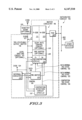
- FIG. 1 illustrates, in block diagram form, integrated circuit 10 in accordance with one embodiment of the present invention
- FIG. 2 illustrates, in schematic diagram form, a contention detection circuit 12 of FIG. 1 in accordance with one embodiment of the present invention
- FIG. 3 illustrates, in block diagram form, integrated circuit 110 in accordance with an alternate embodiment of the present invention
- FIG. 4 illustrates, in schematic diagram form, a contention detection circuit 112 of FIG. 3 in accordance with an alternate embodiment of the present invention.
- FIG. 5 illustrates, in schematic diagram form, a p-portion 117 of level shifting circuit 121 of FIG. 3 in accordance with an alternate embodiment of the present invention.
- FIG. 1 Shown in FIG. 1 is a portion of an integrated circuit 10 for handling buffer contention in accordance with one embodiment of the present invention.
- Integrated circuit 10 comprises a contention detection circuit 12, internal circuitry 14, a terminal or input/output pad 22, and buffer circuitry 16.
- buffer circuitry 16 provides an output signal to input/output pad 22 and comprises a tri-stateable output buffer 18, and a pre-buffer 20 as shown in FIG. 1.
- a tri-stateable output buffer refers to a buffer which is capable of being placed into a high impedance state.
- the buffer is said to be in a "tri-stated" or a "tri-state" condition.
- Contention detection circuit 12, tri-stateable output buffer 18, and pre-buffer 20 are coupled to a non-ground power supply terminal having an external power supply voltage signal (EVDD) 27.
- Internal circuitry 14, pre-buffer 20, and contention detection circuit 12 are coupled to a non-ground power supply terminal having an internal power supply voltage signal (IVDD) 24.
- Data bus 28 is coupled to pre-buffer 20, input/output pad 22, and internal circuitry 14.
- Normal tri-state control signal 32 is coupled to pre-buffer and internal circuitry 14.
- Other control signal 30 is coupled to pre-buffer 20 and internal circuitry 14.
- Contention tri-state control signal 34 is coupled to contention detection circuit 12 and pre-buffer 20. It should be appreciated that contention tri-state control signal 34 may also be coupled to other tri-stateable output buffers as shown in FIG. 1.
- Tri-stateable output buffer 18 is coupled to input/output pad 22.
- Integrated circuit 10 is coupled to a data bus 29 which is in turn coupled to other device(s) 31.
- other device(s) 31 is a computer and input/output pad 22 is coupled to the computer via bus 29.
- integrated circuit 10 is coupled to a schottky diode 25.
- the schottky diode 25 is coupled to EVDD 27 and receives external power supply voltage signal (EVDD) 26 as an input.
- EVDD external power supply voltage signal
- EVDD 27 and IVDD 24 have substantially the same supply voltage during normal operation.
- EVDD 26 and IVDD 24 are both approximately 5 volts or EVDD 26 and IVDD 24 are both approximately 3.3 volts.
- EVDD 26 is powered up (e.g. at approximately 5 volts)
- IVDD 24 is powered up (e.g. at approximately 5 volts)
- EVDD 27 is generated in response to EVDD 26.
- contention detection circuit 12 provides a contention tri-state control signal 34 which is nonactive, active, and thus contention detection circuit 12 does not effect the output of tri-stateable output buffer 18.
- internal circuitry 14 supplies a normal tri-state control signal 32 to pre-buffer circuit 20.
- EVDD 27 may be generated in response to other device(s) 31, and thus a potential buffer contention condition may exist within integrated circuit 10. More specifically other device(s) 31, which is coupled to input/output pad 22, may supply power to input/output pad 22 through bus 29, and thus generate EVDD 27 within integrated circuit 10 when EVDD 26 and IVDD 24 are powered down. For example, if EVDD 26 and IVDD 24 are powered down and other device(s) 31 drives input/output pad 22 to 5 volts, then EVDD 27 is pulled up to approximately the same voltage (i.e.
- tri-stateable output buffer 18 contains an output PMOS pull up transistor and when other device(s) 31 drives input/output pad 22 to 5 volts, the diode formed between the P+ drain and the N-well body of the output PMOS pull up transistor charges the N-well body to a voltage that is a diode drop below the voltage being driven to input/output pad 22. If the gate potential of the output PMOS pull up transistor is low (e.g. approximately 0 volts) and the output PMOS pull up transistor is turned on, then EVDD 27 is pulled up to approximately the same voltage that is being driven to input/output pad 22 because the N-well body of the output PMOS pull up transistor is coupled to EVDD 27.
- contention detection circuit 12 is powered to EVDD 27 by tri-state output buffer 18, and if EVDD 27 is greater than IVDD 24, contention detection circuit 12 supplies a contention tri-state control signal 34 which is active and tri-stateable output buffer 18 is forced to a tri-stated condition.
- tri-stateable output buffer 18 is tri-stated when contention detection circuit 12 detects a predetermined voltage differential between EVDD 27 and IVDD 24.
- schottky diode 25 prevents EVDD 26 from being powered up by EVDD 27 when EVDD 26 and IVDD 24 are powered down, and input/output pad 22 is being powered up by other device(s) 31.
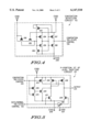
- FIG. 2 Shown in FIG. 2 is a schematic diagram of the contention detection circuit 12 of FIG. 1 in accordance with one embodiment of the present invention.
- Contention detection circuit 12 receives IVDD 24 at a first power supply terminal and EVDD 27 at a second power supply terminal, and outputs contention tri-state control signal 34 at an output terminal, wherein contention tri-state control signal 34 has either a logic high value or a logic low value.
- contention detection circuit 12 comprises an NMOS transistor 40, a PMOS transistor 42, an inverter 44, and an inverter 46.
- a first current electrode of NMOS transistor 40 is coupled to IVDD 24, and a second current electrode of NMOS transistor 40 is coupled to the input of inverter 44 and a first current electrode of PMOS transistor 42.
- EVDD 27 is coupled to the control electrode of NMOS transistor 40, a second current electrode of PMOS transistor 42, inverter 46, and inverter 44.
- the control electrode of PMOS transistor 42 is coupled to the output of inverter 44 and the input of inverter 46.
- a power supply terminal having an external power supply voltage signal (EVSS) 47 is coupled to inverter 44 and inverter 46.
- EVSS 47 is a ground potential.
- the output of inverter 46 is coupled to pre-buffer 20 as shown in FIG. 1.
- the tri-stateable output buffer 18 is not forced into a tri-state condition when the contention tri-state control signal 34 is high.
- EVDD 27 is generated in response to input/output pad 22 being powered up by other device(s) 31 and IVDD 24 and EVDD 26 are powered down, then the output of contention detection circuit 12 is low and the contention tri-state control signal 34 is active or enabled.
- the tri-stateable output buffer 18 is forced into a tri-state condition when the contention tri-state control signal 34 is low.
- NMOS transistor 40 is turned on and inverters 44 and 46 are powered up. If IVDD 24 is powered down, then the input to NMOS transistor 40 is low, PMOS transistor 42 is turned off, and the output of inverter 46 is low.
- Integrated circuit 110 comprises a contention detection circuit 112, internal circuitry 114, a terminal or input/output pad 122, buffer circuitry 116, and a pre-buffer circuit 123.
- buffer circuitry 116 provides an output signal to input/output pad 122 and comprises a tri-stateable output buffer 118, a slew rate control circuit 119, a pre-buffer circuit 120, and a level shifting circuit 121.
- level shifting circuit 121 comprises an N-portion 115 and a P-portion 117 and tri-stateable output buffer 118 has an N-side 113 and a P-side 111.
- Contention detection circuit 112 tri-stateable output buffer 118, slew rate control circuit 119, pre-buffer circuit 120, and level shifting circuit 121 are coupled to a non-ground power supply terminal having an external power supply voltage signal (EVDD) 127.
- Internal circuitry 114, pre-buffer circuit 123, level shifting circuit 121, and contention detection circuit 112 are coupled to a non-ground power supply terminal having an internal power supply voltage signal (IVDD) 124.
- Data bus 128 is coupled to pre-buffer circuit 123, input/output pad 122, and internal circuitry 114.
- Data/normal tri-state control signal 132 is coupled to pre-buffer circuit 123, N-portion 115, and P-portion 117.
- Contention tri-state control signal 134 is coupled to contention detection circuit 112, P-portion 117, and N-portion 115.
- Tri-stateable output buffer 118 is coupled to input/output pad 122.
- Integrated circuit 110 is coupled to a data bus 129 which is in turn coupled to other device(s) 131.
- other device(s) 131 is a computer and input/output pad 122 is coupled to the computer via bus 129.
- integrated circuit 110 is coupled to a schottky diode 125.
- the schottky diode 125 is coupled to external power supply voltage signal (EVDD) 127 and receives external power supply voltage signal (EVDD) 126 as an input.
- EVDD external power supply voltage signal
- integrated circuit 110 is a mixed voltage circuit.
- EVDD 126 may be approximately 5 volts and IVDD 124 may be approximately 3.3 volts.
- level shifting circuit 121 may be required to level shift lower voltage internal data signals and control signals (e.g. 3.3 volt signals) to higher voltages (e.g. 5 volts) for buffer circuitry 116.
- P-portion 117 of level shifting circuit 121 may receive a 3.3 volt data/normal tri-state control signal 132 as an input signal, and then shift this input signal to form a 5.0 volt level-shifted signal. This 5.0 volt level shifted signal is then used to control P-side 111 of tri-stateable output buffer 118, and thus control the output of tri-stateable output buffer 118 to input/output pad 122.
- EVDD 126 is powered up (e.g. at approximately 5 volts) and IVDD 124 is powered up (e.g. at approximately 3.3 volts), and thus EVDD 127 is generated in response to EVDD 126.
- contention detection circuit 112 provides a contention tri-state control signal 134 which is non-active, and thus contention detection circuit 112 does not effect the output of tri-stateable output buffer 118.
- pre-buffer circuit 123 supplies a data/normal tri-state control signal 132 to P-portion 117 and a data/normal tri-state control signal 133 to N-portion 115.
- EVDD 126 when EVDD 126 is powered down (e.g. at approximately 0 volts), and IVDD 124 is powered down (e.g. at approximately 0 volts), EVDD 127 may be generated in response to other device(s) 131, and thus a potential buffer contention condition may exist within integrated circuit 110. More specifically other device(s) 131, which is coupled to input/output pad 122, may supply power to input/output pad 122 through bus 129, and thus generate EVDD 127 within integrated circuit 110 when EVDD 126 and IVDD 124 are powered down.
- EVDD 126 and IVDD 124 are powered down and other device(s) 131 drives input/output pad 122 to 5 volts
- EVDD 127 is pulled up to approximately the same voltage (i.e. approximately 5 volts) as input/output pad 122.
- P-side 111 contains an output PMOS pull up transistor and when other device(s) 131 drives input/output pad 122 to 5 volts, the diode formed between the P+ drain and the N-well body of the output PMOS pull up transistor charges the N-well body to a voltage that is a diode drop below the voltage being driven to input/output pad 122. If the gate potential of the output PMOS pull up transistor is low (e.g.
- contention detection circuit 112 is powered to EVDD 127 by tri-state output buffer 118, and if EVDD 127 is greater than IVDD 124, contention detection circuit 112 supplies a contention tri-state control signal 134 which is active and tri-stateable output buffer 118 is forced to a tri-stated condition.
- tri-stateable output buffer 118 is tri-stated when contention detection circuit 112 detects a predetermined voltage differential between EVDD 127 and IVDD 124. It is also important to note that schottky diode 125 prevents EVDD 126 from being powered up by EVDD 127 when EVDD 126 and IVDD 124 are powered down, and input/output pad 122 is being powered up by other device(s) 131.
- FIG. 4 Shown in FIG. 4 is a schematic diagram of the contention detection circuit 112 of FIG. 3 in accordance with one embodiment of the present invention.
- Contention detection circuit 112 receives IVDD 124 at a first power supply terminal and EVDD 127 at a second power supply terminal, and outputs contention tri-state control signal 134 at an output terminal, wherein contention tri-state control signal 134 has either a logic high value or a logic low value.
- contention detection circuit 112 comprises a PMOS transistor 200, an NMOS transistor 202, a PMOS transistor 203, a PMOS transistor 204, an NMOS transistor 205, an NMOS transistor 206, a PMOS transistor 207, an NMOS transistor 208.
- the control electrode of PMOS transistor 200 and a first current electrode of first PMOS transistor 200 are coupled to IVDD 124.
- the second current electrode of PMOS transistor 200 is coupled to a first current electrode of NMOS transistor 202.
- the second current electrode of NMOS transistor 202 is coupled to the well region of PMOS transistor 200.
- EVDD 127 is coupled to the control electrode of NMOS transistor 202, a first current electrode of PMOS transistor 204, a first current electrode of PMOS transistor 207, a first current electrode of PMOS transistor 203, and to the well region of PMOS transistor 203.
- the second current electrode of PMOS transistor 203 is coupled to the control electrode of PMOS transistor 204, the control electrode of NMOS transistor 205 and a first current electrode of NMOS transistor 206, and the second current electrode of NMOS transistor 202.
- the control electrode of PMOS transistor 203 is coupled to the control electrode of PMOS transistor 207, the control electrode of NMOS transistor 208 and the control electrode of NMOS transistor 206.
- the second current electrode of PMOS transistor 204 is coupled to a first current electrode of NMOS transistor 205 and to the control electrode of PMOS transistor 203.
- a power supply terminal having an external power supply voltage signal (EVSS) 209 is coupled to the second current electrode of NMOS transistor 205, the second current electrode of NMOS transistor 206, and the second current electrode of NMOS transistor 208.
- EVSS 209 is a ground potential as shown in FIG. 4.
- the second current electrode of PMOS transistor 207 and the second current electrode of NMOS transistor 208 are coupled to P-portion 117 and N-portion 115 of FIG. 3.
- the tri-stateable output buffer 118 is not forced into a tri-state condition when the contention tri-state control signal 134 is high.
- EVDD 127 is generated in response to input/output pad 122 being powered up by other device(s) 131 and IVDD 124 and EVDD 126 are powered down, then the output of contention detection circuit 112 is low and the contention tri-state control signal 134 is active or enabled.
- the tri-stateable output buffer 118 is forced into a tri-state condition when the contention tri-state control signal 134 is low.
- NMOS transistor 202 is turned on. If IVDD 124 is powered down, then the gate input to NMOS transistor 205 is low, PMOS transistor 204 is turned on which in turn causes NMOS transistor 208 to turn on and pull contention tri-state control signal 134 low.
- P-portion 117 of level shifting circuit 121 comprises a PMOS transistor 220, a NMOS transistor 221, a PMOS transistor 223, an NMOS transistor 224, an NMOS transistor 227, a PMOS transistor 226, a PMOS transistor 228, an NMOS transistor 229, and an inverter 230.
- the control electrode of PMOS transistor 223, the control electrode of PMOS transistor 220, and the control electrode of NMOS transistor 221 are coupled to contention tri-state control signal 134 of PIG. 4.
- the control electrode of N channel transistor 227 and the input of inverter 230 are coupled to data/normal tri-state control signal 132.
- the output of inverter 230 is coupled to the control electrode of NMOS transistor 229.
- Inverter 230 is coupled to IVDD 124.
- EVSS 209 is coupled to a first current electrode of NMOS transistor 229, a first current electrode of NMOS transistor 227, a first current electrode of NMOS transistor 224, and a first current electrode of NMOS transistor 221.
- a second current electrode of NMOS transistor 221 is coupled to the control electrode of NMOS transistor 224 and a first current electrode of PMOS transistor 220.
- EVDD 127 is coupled to the second current electrode of PMOS transistor 220, a first current electrode of PMOS transistor 223, the well region of PMOS transistor 223, a first current electrode of PMOS transistor 226, and a first current electrode of PMOS transistor 228.
- Output 231 is coupled to the second current electrode of NMOS transistor 229, the second current electrode of PMOS transistor 228, the second current electrode of PMOS transistor 223, and the control electrode of PMOS transistor 226.
- the gate electrode of PMOS transistor 228 is coupled to a second current electrode of NMOS transistor 227, the second current electrode of PMOS transistor 226, and the second current electrode of NMOS transistor 224.
- Contention tri-state control signal 134 and data/normal tri-state control signal 132 are low when IVDD 124 is powered down and EVDD 127 is generated in response to input/output pad 122 being powered up by other device(s) 131. Under these conditions PMOS transistor 223 and NMOS transistor 224 are turned on.
- contention tri-state control signal 134 is high and that turns off PMOS transistor 223 and NMOS transistor 224 so that P-portion 117 does not have a DC current load during normal operation. Therefore, integrated circuits fabricated with P-portion 117 can be used in products requiring low power consumption.
Landscapes
- Physics & Mathematics (AREA)
- Engineering & Computer Science (AREA)
- Computer Hardware Design (AREA)
- Computing Systems (AREA)
- General Engineering & Computer Science (AREA)
- Mathematical Physics (AREA)
- Logic Circuits (AREA)
Abstract
Description
Claims (13)
Priority Applications (2)
| Application Number | Priority Date | Filing Date | Title |
|---|---|---|---|
| US09/114,119 US6147510A (en) | 1998-07-13 | 1998-07-13 | Integrated circuit for handling buffer contention and method thereof |
| US09/636,493 US6380760B1 (en) | 1998-07-13 | 2000-08-11 | Integrated circuit for handling buffer contention and method thereof |
Applications Claiming Priority (1)
| Application Number | Priority Date | Filing Date | Title |
|---|---|---|---|
| US09/114,119 US6147510A (en) | 1998-07-13 | 1998-07-13 | Integrated circuit for handling buffer contention and method thereof |
Related Child Applications (1)
| Application Number | Title | Priority Date | Filing Date |
|---|---|---|---|
| US09/636,493 Continuation US6380760B1 (en) | 1998-07-13 | 2000-08-11 | Integrated circuit for handling buffer contention and method thereof |
Publications (1)
| Publication Number | Publication Date |
|---|---|
| US6147510A true US6147510A (en) | 2000-11-14 |
Family
ID=22353459
Family Applications (2)
| Application Number | Title | Priority Date | Filing Date |
|---|---|---|---|
| US09/114,119 Expired - Fee Related US6147510A (en) | 1998-07-13 | 1998-07-13 | Integrated circuit for handling buffer contention and method thereof |
| US09/636,493 Expired - Lifetime US6380760B1 (en) | 1998-07-13 | 2000-08-11 | Integrated circuit for handling buffer contention and method thereof |
Family Applications After (1)
| Application Number | Title | Priority Date | Filing Date |
|---|---|---|---|
| US09/636,493 Expired - Lifetime US6380760B1 (en) | 1998-07-13 | 2000-08-11 | Integrated circuit for handling buffer contention and method thereof |
Country Status (1)
| Country | Link |
|---|---|
| US (2) | US6147510A (en) |
Cited By (3)
| Publication number | Priority date | Publication date | Assignee | Title |
|---|---|---|---|---|
| US6369613B1 (en) * | 1999-05-10 | 2002-04-09 | Altera Corporation | Input/output drivers |
| US6380760B1 (en) * | 1998-07-13 | 2002-04-30 | Motorola, Inc. | Integrated circuit for handling buffer contention and method thereof |
| US6624682B1 (en) * | 2002-10-09 | 2003-09-23 | Analog Devices, Inc. | Method and an apparatus to actively sink current in an integrated circuit with a floating I/O supply voltage |
Families Citing this family (3)
| Publication number | Priority date | Publication date | Assignee | Title |
|---|---|---|---|---|
| US6845131B1 (en) * | 2000-10-03 | 2005-01-18 | Spectrum Signal Processing Inc. | Differential signaling power management |
| US6983389B1 (en) * | 2002-02-01 | 2006-01-03 | Advanced Micro Devices, Inc. | Clock control of functional units in an integrated circuit based on monitoring unit signals to predict inactivity |
| US6976182B1 (en) * | 2002-02-01 | 2005-12-13 | Advanced Micro Devices, Inc. | Apparatus and method for decreasing power consumption in an integrated circuit |
Citations (3)
| Publication number | Priority date | Publication date | Assignee | Title |
|---|---|---|---|---|
| US5767701A (en) * | 1996-06-28 | 1998-06-16 | Cypress Semiconductor Corp. | Synchronous contention prevention logic for bi-directional signals |
| US5880603A (en) * | 1995-06-02 | 1999-03-09 | Kabushiki Kaisha Toshiba | MOS output buffer with overvoltage protection circuitry |
| US6020757A (en) * | 1998-03-24 | 2000-02-01 | Xilinx, Inc. | Slew rate selection circuit for a programmable device |
Family Cites Families (4)
| Publication number | Priority date | Publication date | Assignee | Title |
|---|---|---|---|---|
| US5576635A (en) * | 1995-02-14 | 1996-11-19 | Advanced Micro Devices, Inc. | Output buffer with improved tolerance to overvoltage |
| US5764077A (en) * | 1996-02-05 | 1998-06-09 | Texas Instruments Incorporated | 5 volt tolerant I/O buffer circuit |
| US5850159A (en) * | 1997-05-12 | 1998-12-15 | Ind Tech Res Inst | High and low speed output buffer with controlled slew rate |
| US6147510A (en) * | 1998-07-13 | 2000-11-14 | Motorola Inc. | Integrated circuit for handling buffer contention and method thereof |
-
1998
- 1998-07-13 US US09/114,119 patent/US6147510A/en not_active Expired - Fee Related
-
2000
- 2000-08-11 US US09/636,493 patent/US6380760B1/en not_active Expired - Lifetime
Patent Citations (3)
| Publication number | Priority date | Publication date | Assignee | Title |
|---|---|---|---|---|
| US5880603A (en) * | 1995-06-02 | 1999-03-09 | Kabushiki Kaisha Toshiba | MOS output buffer with overvoltage protection circuitry |
| US5767701A (en) * | 1996-06-28 | 1998-06-16 | Cypress Semiconductor Corp. | Synchronous contention prevention logic for bi-directional signals |
| US6020757A (en) * | 1998-03-24 | 2000-02-01 | Xilinx, Inc. | Slew rate selection circuit for a programmable device |
Non-Patent Citations (2)
| Title |
|---|
| U.S. Patent Serial No. 08/942,740; Pappert, et al.; "Integrated Circuit Having Buffering Circuitry With Slew Rate Control," filed Oct. 2, 1997. |
| U.S. Patent Serial No. 08/942,740; Pappert, et al.; Integrated Circuit Having Buffering Circuitry With Slew Rate Control, filed Oct. 2, 1997. * |
Cited By (3)
| Publication number | Priority date | Publication date | Assignee | Title |
|---|---|---|---|---|
| US6380760B1 (en) * | 1998-07-13 | 2002-04-30 | Motorola, Inc. | Integrated circuit for handling buffer contention and method thereof |
| US6369613B1 (en) * | 1999-05-10 | 2002-04-09 | Altera Corporation | Input/output drivers |
| US6624682B1 (en) * | 2002-10-09 | 2003-09-23 | Analog Devices, Inc. | Method and an apparatus to actively sink current in an integrated circuit with a floating I/O supply voltage |
Also Published As
| Publication number | Publication date |
|---|---|
| US6380760B1 (en) | 2002-04-30 |
Similar Documents
| Publication | Publication Date | Title |
|---|---|---|
| EP0706267B1 (en) | An all-CMOS high-impedance output buffer for a bus driven by multiple power-supply voltages | |
| EP0614279B1 (en) | Overvoltage tolerant output buffer circuit | |
| KR100282287B1 (en) | Protection against overvoltage | |
| US7397296B1 (en) | Power supply detection circuit biased by multiple power supply voltages for controlling a signal driver circuit | |
| EP0765035A2 (en) | Output circuit | |
| US6911860B1 (en) | On/off reference voltage switch for multiple I/O standards | |
| US6879191B2 (en) | Voltage mismatch tolerant input/output buffer | |
| JPH07170168A (en) | Output circuit and operation method | |
| EP0260389A2 (en) | Off-chip driver circuits | |
| US6674304B1 (en) | Output buffer circuit and method of operation | |
| US6184700B1 (en) | Fail safe buffer capable of operating with a mixed voltage core | |
| US5828231A (en) | High voltage tolerant input/output circuit | |
| KR100363381B1 (en) | Two-supply protection circuit | |
| EP1081860B1 (en) | Single gate oxide output buffer stage with a cascaded transistor | |
| WO1998037634A1 (en) | Voltage tolerant input/output buffer | |
| US7521965B2 (en) | 5 volt tolerant IO scheme using low-voltage devices | |
| US6265931B1 (en) | Voltage reference source for an overvoltage-tolerant bus interface | |
| US6147510A (en) | Integrated circuit for handling buffer contention and method thereof | |
| US20080106836A1 (en) | Io clamping circuit method utilizing output driver transistors | |
| EP0699998B1 (en) | Semiconductor integrated circuit | |
| US5276366A (en) | Digital voltage level translator circuit | |
| US6472906B2 (en) | Open drain driver having enhanced immunity to I/O ground noise | |
| US6940334B2 (en) | Methods and systems for generating interim voltage supplies | |
| US11411561B2 (en) | Semiconductor circuit and semiconductor system | |
| US5825221A (en) | Output circuit of semiconductor device |
Legal Events
| Date | Code | Title | Description |
|---|---|---|---|
| AS | Assignment |
Owner name: MOTOROLA, INC., ILLINOIS Free format text: ASSIGNMENT OF ASSIGNORS INTEREST;ASSIGNOR:PAPPERT, BERNARD J.;REEL/FRAME:009316/0826 Effective date: 19980707 |
|
| FPAY | Fee payment |
Year of fee payment: 4 |
|
| AS | Assignment |
Owner name: FREESCALE SEMICONDUCTOR, INC., TEXAS Free format text: ASSIGNMENT OF ASSIGNORS INTEREST;ASSIGNOR:MOTOROLA, INC.;REEL/FRAME:015698/0657 Effective date: 20040404 Owner name: FREESCALE SEMICONDUCTOR, INC.,TEXAS Free format text: ASSIGNMENT OF ASSIGNORS INTEREST;ASSIGNOR:MOTOROLA, INC.;REEL/FRAME:015698/0657 Effective date: 20040404 |
|
| AS | Assignment |
Owner name: CITIBANK, N.A. AS COLLATERAL AGENT, NEW YORK Free format text: SECURITY AGREEMENT;ASSIGNORS:FREESCALE SEMICONDUCTOR, INC.;FREESCALE ACQUISITION CORPORATION;FREESCALE ACQUISITION HOLDINGS CORP.;AND OTHERS;REEL/FRAME:018855/0129 Effective date: 20061201 Owner name: CITIBANK, N.A. AS COLLATERAL AGENT,NEW YORK Free format text: SECURITY AGREEMENT;ASSIGNORS:FREESCALE SEMICONDUCTOR, INC.;FREESCALE ACQUISITION CORPORATION;FREESCALE ACQUISITION HOLDINGS CORP.;AND OTHERS;REEL/FRAME:018855/0129 Effective date: 20061201 |
|
| FPAY | Fee payment |
Year of fee payment: 8 |
|
| AS | Assignment |
Owner name: CITIBANK, N.A., AS COLLATERAL AGENT,NEW YORK Free format text: SECURITY AGREEMENT;ASSIGNOR:FREESCALE SEMICONDUCTOR, INC.;REEL/FRAME:024397/0001 Effective date: 20100413 Owner name: CITIBANK, N.A., AS COLLATERAL AGENT, NEW YORK Free format text: SECURITY AGREEMENT;ASSIGNOR:FREESCALE SEMICONDUCTOR, INC.;REEL/FRAME:024397/0001 Effective date: 20100413 |
|
| REMI | Maintenance fee reminder mailed | ||
| LAPS | Lapse for failure to pay maintenance fees | ||
| STCH | Information on status: patent discontinuation |
Free format text: PATENT EXPIRED DUE TO NONPAYMENT OF MAINTENANCE FEES UNDER 37 CFR 1.362 |
|
| FP | Lapsed due to failure to pay maintenance fee |
Effective date: 20121114 |
|
| AS | Assignment |
Owner name: FREESCALE SEMICONDUCTOR, INC., TEXAS Free format text: PATENT RELEASE;ASSIGNOR:CITIBANK, N.A., AS COLLATERAL AGENT;REEL/FRAME:037354/0225 Effective date: 20151207 Owner name: FREESCALE SEMICONDUCTOR, INC., TEXAS Free format text: PATENT RELEASE;ASSIGNOR:CITIBANK, N.A., AS COLLATERAL AGENT;REEL/FRAME:037356/0143 Effective date: 20151207 Owner name: FREESCALE SEMICONDUCTOR, INC., TEXAS Free format text: PATENT RELEASE;ASSIGNOR:CITIBANK, N.A., AS COLLATERAL AGENT;REEL/FRAME:037356/0553 Effective date: 20151207 |
|
| AS | Assignment |
Owner name: NXP B.V., NETHERLANDS Free format text: PATENT RELEASE;ASSIGNORS:MORGAN STANLEY SENIOR FUNDING, INC., AS GLOBAL COLLATERAL AGENT;MORGAN STANLEY SENIOR FUNDING, INC., AS RCF ADMINISTRATIVE AGENT;MORGAN STANLEY SENIOR FUNDING, INC., AS THE NOTES COLLATERAL AGENT;REEL/FRAME:039428/0845 Effective date: 20160712 |
|
| AS | Assignment |
Owner name: VLSI TECHNOLOGY LLC, DELAWARE Free format text: ASSIGNMENT OF ASSIGNORS INTEREST;ASSIGNOR:FREESCALE SEMICONDUCTOR, INC.;REEL/FRAME:039490/0701 Effective date: 20160816 |
|
| AS | Assignment |
Owner name: VLSI TECHNOLOGY LLC, DELAWARE Free format text: CORRECTIVE ASSIGNMENT TO CORRECT THE SIGNATURE PAGE PREVIOUSLY RECORDED AT REEL: 039490 FRAME: 0701. ASSIGNOR(S) HEREBY CONFIRMS THE ASSIGNMENT;ASSIGNOR:FREESCALE SEMICONDUCTOR, INC.;REEL/FRAME:040014/0173 Effective date: 20160816 |
|
| AS | Assignment |
Owner name: NXP USA, INC. F/K/A FREESCALE SEMICONDUCTOR, INC., Free format text: RELEASE BY SECURED PARTY;ASSIGNOR:MORGAN STANLEY SENIOR FUNDING, INC.;REEL/FRAME:042610/0451 Effective date: 20170502 |