US6146966A - Process for forming a capacitor incorporated in a semiconductor device - Google Patents
Process for forming a capacitor incorporated in a semiconductor device Download PDFInfo
- Publication number
- US6146966A US6146966A US08/859,210 US85921097A US6146966A US 6146966 A US6146966 A US 6146966A US 85921097 A US85921097 A US 85921097A US 6146966 A US6146966 A US 6146966A
- Authority
- US
- United States
- Prior art keywords
- temperature
- amorphous silicon
- silicon film
- film
- capacitor
- Prior art date
- Legal status (The legal status is an assumption and is not a legal conclusion. Google has not performed a legal analysis and makes no representation as to the accuracy of the status listed.)
- Expired - Lifetime
Links
Images

Classifications
-
- H—ELECTRICITY
- H10—SEMICONDUCTOR DEVICES; ELECTRIC SOLID-STATE DEVICES NOT OTHERWISE PROVIDED FOR
- H10B—ELECTRONIC MEMORY DEVICES
- H10B12/00—Dynamic random access memory [DRAM] devices
-
- H—ELECTRICITY
- H10—SEMICONDUCTOR DEVICES; ELECTRIC SOLID-STATE DEVICES NOT OTHERWISE PROVIDED FOR
- H10D—INORGANIC ELECTRIC SEMICONDUCTOR DEVICES
- H10D1/00—Resistors, capacitors or inductors
- H10D1/60—Capacitors
- H10D1/68—Capacitors having no potential barriers
- H10D1/692—Electrodes
- H10D1/711—Electrodes having non-planar surfaces, e.g. formed by texturisation
- H10D1/712—Electrodes having non-planar surfaces, e.g. formed by texturisation being rough surfaces, e.g. using hemispherical grains
-
- H—ELECTRICITY
- H10—SEMICONDUCTOR DEVICES; ELECTRIC SOLID-STATE DEVICES NOT OTHERWISE PROVIDED FOR
- H10B—ELECTRONIC MEMORY DEVICES
- H10B12/00—Dynamic random access memory [DRAM] devices
- H10B12/01—Manufacture or treatment
- H10B12/02—Manufacture or treatment for one transistor one-capacitor [1T-1C] memory cells
- H10B12/03—Making the capacitor or connections thereto
- H10B12/033—Making the capacitor or connections thereto the capacitor extending over the transistor
Definitions
- the present invention relates to a process for manufacturing a semiconductor device, and more specifically to a process for forming a capacitor incorporated in a semiconductor device.
- DRAM dynamic random access memory
- the integration density is increased more and more, namely, a memory capacity is increased more and more in a semiconductor memory.
- a memory capacity is increased more and more in a semiconductor memory.
- it is not allowed to increase the size of a semiconductor device chip. Because of this, how small a memory cell is formed, is an important problem to be solved on the semiconductor device.
- the memory cell having the stacked capacitor As compared with the memory cell having the trench capacitor, the memory cell having the stacked capacitor has an excellent soft-error resistance and an advantage in which no damage is given to a silicon substrate. Therefore, the stacked capacitor type memory cell is expected as next generation memory cell structure.
- a stacked capacitor formed by utilizing a HSG (hemi-spherical grain) technology As the stacked capacitor, there is proposed a stacked capacitor formed by utilizing a HSG (hemi-spherical grain) technology.
- This type of stacked capacitor is constituted of a capacitor lower plate (storage node capacitor cell plate), a capacitor insulator film and a capacitor upper plate (common plate), the capacitor lower plate being electrically connected through a contact hole formed in an interlayer insulator film, to a MOSFET (metal-oxide-semiconductor field effect transistor) formed in a semiconductor substrate.
- MOSFET metal-oxide-semiconductor field effect transistor
- Japan Patent Application Pre-examination Publication No. JP-A-5-110023 proposes to deposit an amorphous silicon film through a natural oxide film on a silicon film, and to conduct a heat treatment to cause migration in a surface of the amorphous silicon film, so that a surface-roughed polysilicon film having a concave-convex upper surface is formed.
- This JP-A-5-110023 is so featured in that the formation of the concaves and convexes formed by the HSG technology is limited to only a top surface of the polysilicon film, and therefore, the increase of the capacitance inevitably has certain limit.
- Japanese Patent Application Pre-examination Publication No. JP-A-5-315543 proposes a process for forming, by the HSG technology, concaves and convexes not only on a top surface of a capacitor lower plate but also on a side surface of the capacitor lower plate.
- this proposed process after an amorphous silicon film deposited by a CVD (chemical vapor deposition) process is patterned by a selective etching, the patterned amorphous silicon film is heat-treated in an inert gas or vacuum atmosphere, so that the amorphous silicon film is crystallized into a polysilicon film.
- CVD chemical vapor deposition
- a so called a “crystal nucleation” has been proposed in which SiH 4 or the like is irradiated to the top surface and the side surface of the amorphous silicon to form nuclei on these surfaces, and then, an annealing is conducted to form the concaves and convexes on the top surface and the side surface of the amorphous silicon. More specifically, in this "crystal nucleation", an amorphous silicon film is formed to electrically connect to a semiconductor device element such as a MOSFET formed in a semiconductor substrate, through a contact hole selectively formed through an interlayer insulator film, and the amorphous silicon film is patterned to form a capacitor lower plate.
- a semiconductor device element such as a MOSFET formed in a semiconductor substrate
- a natural oxide film remaining on a surface of the capacitor lower plate is removed by use of HF of the like, and thereafter, SiH 4 is irradiated onto the capacitor lower plate within a reaction chamber which is maintained at a predetermined temperature. After irradiation of SiH 4 , an annealing is conducted for a predetermined length of time.
- the capacitor lower plate having the concaves and convexes formed on not only the top surface but also the side surface in accordance with the HSG technology.
- crystal nucleation In the above mentioned “crystal nucleation" process, however, it was observed that, a crystal grows from a boundary between the capacitor lower plate film and the interlayer insulator film, and this crystallization reaches to the exposed top surface and the exposed side surface of the capacitor lower plate before the concaves and convexes are formed on the top surface and the side surface of the capacitor lower plate. If the crystallization reaches to the top surface and the side surface, the HSG formation process no longer advances, with the result that an expected increase of the surface area of the capacitor lower plate cannot be obtained. Actually, in the same wafer, some memory chips can obtain an expected increase of the surface area of the capacitor lower plate, but other memory chips cannot obtain the expected increase of the surface area of the capacitor lower plate, with the result that the production yield is low.
- Another object of the present invention is to provide a process for manufacturing a semiconductor device, which can minimize, in the "crystal nucleation" process, a crystallization occurring from a boundary between an amorphous semiconductor film and an interlayer insulator film in contact therewith.
- Still another object of the present invention is to provide a process for forming a capacitor incorporated in a semiconductor device, which has a capacitor lower plate having an increased surface area.
- the second temperature is not higher than 600° C.
- the first temperature is not lower than 530° C. and is lower than the second temperature by not less than 5° C.
- a process for forming a capacitor which is formed on an interlayer insulator film and which is electrically connected to a semiconductor substrate through a contact hole formed through the interlayer insulator film, the process comprising the steps of forming a patterned amorphous silicon film to fill the contact hole and to partially cover the interlayer insulator film, irradiating a crystal nucleus forming gas onto the patterned amorphous silicon film at a temperature which makes a growth rate of crystals growing from a boundary between the patterned amorphous silicon film and the interlayer insulator film, lower than that in a succeeding annealing step, so that crystal nuclei are formed on a surface of the patterned amorphous silicon film, annealing the patterned amorphous silicon film so that hemi-spherical silicon grains are formed from the crystal nuclei on the surface of the patterned amorphous silicon film, forming a capacitor dielectric film to cover the hemi-s
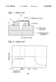
- FIG. 1 is a diagrammatic section view of the capacitor lower plate formed in accordance with the temperature sequence as shown in FIG. 2;
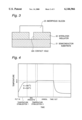
- FIG. 2 is a graph showing the temperature sequence, for illustrating the prior art process for forming the HSG structure capacitor lower plate
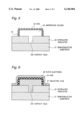
- FIG. 3 is a diagrammatic section view of the capacitor lower plate to be treated in accordance with the temperature sequence of the process in accordance with the present invention for forming the HSG structure capacitor lower plate;
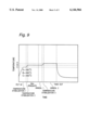
- FIG. 4 is a graph showing the temperature sequence of a first embodiment of the process in accordance with the present invention for forming the HSG structure capacitor lower plate;
- FIG. 5 is a diagrammatic section view of the capacitor lower plate on which the hemi-spherical grains are formed on the amorphous silicon film in accordance with the temperature sequence of the process in accordance with the present invention for forming the HSG structure capacitor lower plate;
- FIG. 6 is a diagrammatic section view of the HSG structure capacitor completed in accordance with the process in accordance with the present invention for forming the HSG structure capacitor lower plate;
- FIG. 7 is a graph showing the temperature sequence of a second embodiment of the process in accordance with the present invention for forming the HSG structure capacitor lower plate;
- FIG. 8 is a graph showing the temperature sequence of a third embodiment of the process in accordance with the present invention for forming the HSG structure capacitor lower plate.
- FIG. 9 is a graph showing the temperature sequence of a first embodiment of the process in accordance with the present invention for forming the HSG structure capacitor lower plate.
- a capacitor lower plate to be formed with hemi-spherical grains is designated with Reference Numeral 26.
- the capacitor lower plate 26 is a patterned amorphous silicon film.
- an interlayer insulator film 22 is formed, and a contact hole 22A is selectively formed to penetrate through the interlayer insulator film 22 and to partially expose the semiconductor substrate 21.
- the interlayer insulator film 22 is formed of BPSG (borophosphosilicate glass) or NSG (non-doped silicate glass).
- an impurity-doped, for example, phosphorus-doped, amorphous silicon 23 is formed to fill the contact hole 22A and to cover the interlayer 22, and then, is patterned to have an exposed side surface and an exposed top surface.
- a natural oxide film covers the surface of the amorphous silicon film 23. Therefore, if the surface of the amorphous silicon film 23 is covered with the natural oxide film, the natural oxide film is removed by an etching or the like.
- the semiconductor substrate thus prepared is introduced into a reaction chamber, and a treatment is conducted at a temperature shown in FIG. 2 which illustrate a temperature sequence for processing the semiconductor substrate.
- the semiconductor substrate is heated to a temperature of about 550° C. to 570° C., and then, is maintained at this temperature.
- SiH 4 is introduced into the reaction chamber, so that SiH 4 is irradiated onto the amorphous silicon film for a predetermined constant period of time.
- nuclei composed of silicon atoms are formed on the exposed top surface and the exposed side surface of the patterned amorphous silicon film.
- the patterned amorphous silicon film is annealed at the same temperature for another predetermined period of time.
- this annealing process on the exposed top surface and the exposed side surface of the patterned amorphous silicon film, migration of amorphous silicon occurs so that silicon atoms in the neighborhood of each nucleus aggregate or flocculate toward each nucleus, with the result that hemi-spherical silicon crystalline grains are formed on the exposed top surface and the exposed side surface of the patterned amorphous silicon film.
- the semiconductor substrate having the thus formed hemi-spherical silicon crystalline grains is taken out from the reaction chamber.
- a dielectric film and a common plate electrode both not shown
- the phenomenon was found out that, a crystal, different from the hemi-spherical grains, grows from a boundary between the amorphous silicon and the interlayer insulator, and if the crystal reaches a top surface and a side surface of the amorphous silicon, no hemi-spherical grain is formed on a surface of the crystallized portion.
- the co-inventors of the present application found out that the crystallization of the amorphous silicon starting from the boundary between the amorphous silicon and the interlayer insulator film can be suppressed or retarded by changing the temperature sequence. On the basis of this finding, the co-inventors of the present application propose here an improved process for forming a capacitor component.
- FIGS. 3, 4, 5 and 6 a first embodiment of the process in accordance with the present invention for forming a capacitor component, which can be used as a cell capacitor for the stacked capacitor structure DRAM memory cell, will be described with reference to FIGS. 3, 4, 5 and 6.
- FIG. 3 illustrates a condition in which on a semiconductor substrate 21 (having for example MOSFTs (not shown) previously formed therein for the purpose of forming memory cells), there are formed an interlayer insulator film 22 (which is formed of for example BPSG or NSG) having a contact hole 22A selectively formed to penetrate through the interlayer insulator film 22 and to partially expose the semiconductor substrate 21, and a patterned phosphorus-doped amorphous silicon 23 formed to fill the contact hole 22A and to partially cover the interlayer 22 and to have an exposed side surface and an exposed top surface.
- the semiconductor substrate thus prepared is introduced into a reaction chamber.
- a treatment for the HSG formation is performed in accordance with the temperature sequence as shown in FIG. 4.
- the semiconductor substrate is heated to a temperature B of about 555° C. (which is lower than an annealing temperature A of about 560° C. by 5° C.) ("TEMPERATURE STABILIZATION 1" in FIG. 4).
- SiH 4 is introduced into the reaction chamber as a gas for forming crystal nuclei composed of silicon atoms, so that SiH 4 is irradiated onto the phosphorus-doped amorphous silicon film 23. Introduction of SiH 4 is performed for 20 minutes for example.
- the reaction chamber is maintained at a vacuum degree of for example 0.11997 Pa (0.9 mTorr) during a period of time in which SiH 4 is introduced.
- a vacuum degree for example 0.11997 Pa (0.9 mTorr) during a period of time in which SiH 4 is introduced.
- the temperature of the semiconductor substrate is elevated to the temperature A of about 560° C. At this time, a transient time of about five minutes is required until the temperature of the semiconductor substrate has been stabilized at the temperature A ("TEMPERATURE STABILIZATION 2" in FIG. 4). If the temperature of the semiconductor substrate is put in the stabilized temperature A, the semiconductor substrate starts to be annealed in the reaction chamber. Therefore, the temperature A indicates a stabilized temperature in the annealing step. This annealing was conducted for 35 minutes.
- the semiconductor substrate formed with the hemi-spherical grains (HSG) by the above mentioned annealing process is taken out from the reaction chamber, and then, is cooled down, and thereafter, is introduced into another reaction chamber (not shown).
- a silicon oxide film or a silicon nitride film having a thickness of 5 nm to 8 nm is formed on the hemi-spherical grains 24 by a conventional process, so as to form a dielectric film 27 of the capacitor. Furthermore, a polysilicon film is deposited to cover the dielectric film 27 to form a capacitor upper plate, namely, a common plate electrode 28. Thus, a capacitor is constituted of the lower plate 22 having the hemi-spherical grains 24, the dielectric film 27 and the upper plate 28. Incidentally, if a heat treatment is conducted after formation of the hemi-spherical grains (HSG), the amorphous silicon 23 becomes polysilicon.
- HSG hemi-spherical grains
- FIG. 7 there is shown a temperature sequence illustrating a second embodiment of the process in accordance with the present invention for forming the HSG structure capacitor lower plate.
- the second embodiment is characterized in that the annealing temperature A' in the annealing step is set to 570° C., which is somewhat higher than that of the first embodiment, and the stabilized temperature B at the time of irradiating SiH 4 is set to 560° C., which is lower than the annealing temperature A' by 10° C.
- the SiH 4 irradiating time and the annealing time were about 15 minutes and about 20 minutes, respectively.
- the stabilized temperature B at the time of irradiating SiH 4 and the annealing temperature A' are made higher than those in the first embodiment, it was possible to prevent a crystal growing in the amorphous silicon from reaching the surface of the amorphous silicon film before the hemi-spherical grains are formed on the whole exposed surface of the amorphous silicon film, similarly to the first embodiment.
- the crystal nucleus formation processing time and the annealing time can be shortened in comparison with the first embodiment, and furthermore, the throughput can be improved.
- This third embodiment is characterized in that the temperature is caused to change over three steps from the moment the semiconductor substrate is introduced into the reaction chamber to the moment the annealing is completed.
- the semiconductor substrate is heated to a temperature C of about 550° C., which is lower than by 5° C. the stabilized temperature B of about 555° C. at the time of irradiating SiH 4 , and after the temperature of the semiconductor substrate is stabilized at the temperature C, the semiconductor substrate is heated to the stabilized temperature B for irradiating SiH 4 , and stabilized at the temperature B. During a period that the temperature of the semiconductor substrate is maintained at the stabilized temperature B, SiH 4 is introduced and irradiated. After the irradiation of SiH 4 , the semiconductor substrate is heated to elevate by 5° C. to reach the anneal temperature A of about 560° C.
- the third embodiment is characterized in that the semiconductor substrate is preliminary heated before the irradiation of SiH 4 , with the result that the semiconductor substrate can be easily heated to the stabilized temperature B for the crystal nucleus formation processing. Therefore, it is considered that the temperature C is lower than the stabilized temperature B by a value preferably not less than 5° C. but not greater than 10° C. so that the semiconductor substrate can be easily heated to the crystal nucleus formation processing temperature.
- the crystallization rate of amorphous silicon becomes exponentially quick if the temperature exceeds a certain temperature.
- about 30 minutes are required until it reaches the temperature B for the SiH 4 irradiation, namely, as the period of "TEMPERATURE STABILIZATION 1", and in this period of time, in fact, crystallization advances in the amorphous silicon 23.
- a temperature sequence of a fourth embodiment of the process in accordance with the present invention for forming the HSG structure capacitor lower plate will be described with reference to FIG. 9.
- This fourth embodiment is characterized in that the temperature is caused to change over two steps in the annealing process.
- the semiconductor substrate is annealed at the same temperature as that the stabilized temperature B for irradiating SiH 4 , for about ten minutes, and succeedingly, in an "ANNEAL 2", the semiconductor substrate is heated to elevate by 5° C. to reach the annealing temperature A, and thereafter, the semiconductor substrate is annealed at the temperature A for about 25 minutes.
- the silicon atoms are supplied to each crystal nucleus from the amorphous silicon 23.
- the supply amount is also at constant per time.
- Silicon atoms are deposited on a surface of the hemi-spherical silicon crystalline grains because of the migration, with the result that the size or diameter of the hemi-spherical silicon crystalline grains becomes large. Therefore, if the supply amount of silicon atoms is at constant, the grain diameter increasing rate or speed lowers with an increase of the surface area of the hemi-spherical silicon crystalline grains 24. Thus, the grain diameter increasing rate or speed of the hemi-spherical silicon crystalline grains 24 lowers with the lapse of time.
- the HSG formation is caused to advance while maintaining the crystal growth rate at a low level, and if the grain diameter of the hemi-spherical silicon crystalline grains 24 becomes large to some degree, the anneal is transited to the "ANNEAL 2" so that the temperature is elevated to the temperature A. If the temperature is elevated to the temperature A, since the supply amount of silicon atoms increases, the growth of the hemi-spherical silicon crystalline grains 24 is accelerated so that the grains 24 can be further enlarged.
- the stabilized temperature B for irradiating SiH 4 at a temperature lower than the annealing temperature A or A', advancement of the crystallization in the amorphous silicon, starting from the boundary between the amorphous silicon and the interlayer insulator film, can be suppressed or retarded during the process of the SiH 4 irradiation, namely during the crystal nucleus formation process.
- the annealing temperature is not higher than 600° C. and the stabilized temperature B for irradiating the crystal nucleus forming gas is not lower than 530° C.
- the crystals growing into the amorphous silicon from the boundary between the amorphous silicon and the interlayer insulator does not reach the surface of the amorphous silicon film in the annealing process.
- the crystal growth greatly depends upon both the temperature and the lapse of time.
- the crystals growing from the boundary between the amorphous silicon and the interlayer insulator continues to grow in the amorphous silicon over the whole period of the crystal nucleus formation process and the annealing process for forming the hemi-spherical grains. Therefore, during the crystal nucleus formation process, the crystals starts to grow from the boundary between the amorphous silicon and the interlayer insulator and continues to grow in the amorphous silicon, but although the silicon nuclei are formed on the surface of the amorphous silicon, the hemi-spherical grains do not grow from the silicon nuclei.
- the stabilized temperature B for irradiating the crystal nucleus forming gas is lower than 530° C.
- the crystal nuclei formed of silicon atoms could not be formed on the surface of the amorphous silicon film.
- the annealing temperature A is higher than 600° C., a crystal generates in the inside of the amorphous silicon film, and it is no longer possible to control the growth of the crystal in the amorphous silicon film.
- the stabilized temperature B for irradiating the crystal nucleus forming gas is lower than the annealing temperature A by not less than 5° C., although crystals generate, the growth of the generated crystals can be sufficiently suppressed or retarded in the crystal nucleus forming process.
- the stabilized temperature B for irradiating the crystal nucleus forming gas is lower than the annealing temperature A by less than 5° C., the crystals growing into the amorphous silicon from the boundary between the amorphous silicon and the interlayer insulator could not satisfactory be prevented from reaching the surface of the amorphous silicon film in the annealing process.
- silane (SiH 4 ) was irradiated as a source gas for forming the crystal nuclei, but in place of the silane, disilane (Si 2 H 6 ) or trisilane (Si 3 H 8 ) can be used.
- As (arsenic) or B (boron) can be used in place of phosphorus.
- the process in accordance with the present invention can suppress or retard the growth of the crystals starting from the boundary between the amorphous silicon film and the interlayer insulator film and growing in the amorphous silicon film, in the process for forming the hemi-spherical silicon grains on the basis of the "crystal nucleation" process, with the result that it is possible to prevent formation of hemi-spherical silicon grains from being obstructed by the growth of the crystals growing in the amorphous silicon film. Accordingly, it is possible to form a capacitor lower plate having a large surface area
Landscapes
- Semiconductor Memories (AREA)
- Semiconductor Integrated Circuits (AREA)
Abstract
Description
Claims (6)
Applications Claiming Priority (2)
| Application Number | Priority Date | Filing Date | Title |
|---|---|---|---|
| JP8125698A JP2795316B2 (en) | 1996-05-21 | 1996-05-21 | Method for manufacturing semiconductor device |
| JP8-125698 | 1996-05-21 |
Publications (1)
| Publication Number | Publication Date |
|---|---|
| US6146966A true US6146966A (en) | 2000-11-14 |
Family
ID=14916505
Family Applications (1)
| Application Number | Title | Priority Date | Filing Date |
|---|---|---|---|
| US08/859,210 Expired - Lifetime US6146966A (en) | 1996-05-21 | 1997-05-20 | Process for forming a capacitor incorporated in a semiconductor device |
Country Status (3)
| Country | Link |
|---|---|
| US (1) | US6146966A (en) |
| JP (1) | JP2795316B2 (en) |
| KR (1) | KR100246278B1 (en) |
Cited By (5)
| Publication number | Priority date | Publication date | Assignee | Title |
|---|---|---|---|---|
| FR2782844A1 (en) * | 1998-08-28 | 2000-03-03 | Samsung Electronics Co Ltd | METHOD FOR MANUFACTURING A CAPACITOR USING SILICON IN THE FORM OF HEMISPHERIC GRAINS |
| US20030176077A1 (en) * | 2002-03-13 | 2003-09-18 | Lee Dong Ho | Method for fabricating semiconductor capacitors |
| US6713371B1 (en) | 2003-03-17 | 2004-03-30 | Matrix Semiconductor, Inc. | Large grain size polysilicon films formed by nuclei-induced solid phase crystallization |
| US20050072976A1 (en) * | 2003-10-07 | 2005-04-07 | Matrix Semiconductor, Inc. | Uniform seeding to control grain and defect density of crystallized silicon for use in sub-micron thin film transistors |
| US20220319846A1 (en) * | 2021-04-06 | 2022-10-06 | Tokyo Electron Limited | Method of crystallizing amorphous silicon film and deposition apparatus |
Families Citing this family (2)
| Publication number | Priority date | Publication date | Assignee | Title |
|---|---|---|---|---|
| JP3187364B2 (en) | 1998-02-19 | 2001-07-11 | 日本電気株式会社 | Method for manufacturing semiconductor device |
| CN118475119A (en) * | 2024-06-07 | 2024-08-09 | 福建省晋华集成电路有限公司 | Semiconductor device and method for manufacturing the same |
Citations (8)
| Publication number | Priority date | Publication date | Assignee | Title |
|---|---|---|---|---|
| JPH05110023A (en) * | 1991-03-25 | 1993-04-30 | Miyazaki Oki Electric Co Ltd | Method for formation of lower electrode of capacitor |
| JPH05315543A (en) * | 1992-05-08 | 1993-11-26 | Nec Corp | Semiconductor device and manufacture thereof |
| JPH0714797A (en) * | 1993-06-03 | 1995-01-17 | Micron Semiconductor Inc | Method for uniform doping of hemispherical grained polycrystalline silicon |
| US5385863A (en) * | 1991-06-21 | 1995-01-31 | Nec Corporation | Method of manufacturing polysilicon film including recrystallization of an amorphous film |
| US5691228A (en) * | 1996-01-18 | 1997-11-25 | Micron Technology, Inc. | Semiconductor processing method of making a hemispherical grain (HSG) polysilicon layer |
| US5721171A (en) * | 1996-02-29 | 1998-02-24 | Micron Technology, Inc. | Method for forming controllable surface enhanced three dimensional objects |
| US5759262A (en) * | 1995-11-03 | 1998-06-02 | Micron Technology, Inc. | Method of forming hemispherical grained silicon |
| US5770500A (en) * | 1996-11-15 | 1998-06-23 | Micron Technology, Inc. | Process for improving roughness of conductive layer |
-
1996
- 1996-05-21 JP JP8125698A patent/JP2795316B2/en not_active Expired - Fee Related
-
1997
- 1997-05-20 US US08/859,210 patent/US6146966A/en not_active Expired - Lifetime
- 1997-05-21 KR KR1019970020680A patent/KR100246278B1/en not_active Expired - Fee Related
Patent Citations (8)
| Publication number | Priority date | Publication date | Assignee | Title |
|---|---|---|---|---|
| JPH05110023A (en) * | 1991-03-25 | 1993-04-30 | Miyazaki Oki Electric Co Ltd | Method for formation of lower electrode of capacitor |
| US5385863A (en) * | 1991-06-21 | 1995-01-31 | Nec Corporation | Method of manufacturing polysilicon film including recrystallization of an amorphous film |
| JPH05315543A (en) * | 1992-05-08 | 1993-11-26 | Nec Corp | Semiconductor device and manufacture thereof |
| JPH0714797A (en) * | 1993-06-03 | 1995-01-17 | Micron Semiconductor Inc | Method for uniform doping of hemispherical grained polycrystalline silicon |
| US5759262A (en) * | 1995-11-03 | 1998-06-02 | Micron Technology, Inc. | Method of forming hemispherical grained silicon |
| US5691228A (en) * | 1996-01-18 | 1997-11-25 | Micron Technology, Inc. | Semiconductor processing method of making a hemispherical grain (HSG) polysilicon layer |
| US5721171A (en) * | 1996-02-29 | 1998-02-24 | Micron Technology, Inc. | Method for forming controllable surface enhanced three dimensional objects |
| US5770500A (en) * | 1996-11-15 | 1998-06-23 | Micron Technology, Inc. | Process for improving roughness of conductive layer |
Non-Patent Citations (1)
| Title |
|---|
| British Search Report, dated Jul. 30, 1997. * |
Cited By (12)
| Publication number | Priority date | Publication date | Assignee | Title |
|---|---|---|---|---|
| FR2782844A1 (en) * | 1998-08-28 | 2000-03-03 | Samsung Electronics Co Ltd | METHOD FOR MANUFACTURING A CAPACITOR USING SILICON IN THE FORM OF HEMISPHERIC GRAINS |
| US6333227B1 (en) * | 1998-08-28 | 2001-12-25 | Samsung Electronics Co., Ltd. | Methods of forming hemispherical grain silicon electrodes by crystallizing the necks thereof |
| NL1012544C2 (en) * | 1998-08-28 | 2004-05-26 | Samsung Electronics Co Ltd | Process for manufacturing a capacitor using hemispherical granular silicon. |
| US20030176077A1 (en) * | 2002-03-13 | 2003-09-18 | Lee Dong Ho | Method for fabricating semiconductor capacitors |
| US6706642B2 (en) * | 2002-03-13 | 2004-03-16 | Hynix Semiconductor Inc. | Method for fabricating semiconductor capacitors |
| US6713371B1 (en) | 2003-03-17 | 2004-03-30 | Matrix Semiconductor, Inc. | Large grain size polysilicon films formed by nuclei-induced solid phase crystallization |
| US20070105305A1 (en) * | 2003-03-17 | 2007-05-10 | Shuo Gu | Method to form large grain size polysilicon films by nuclei-induced solid phase crystallization |
| US7361578B2 (en) | 2003-03-17 | 2008-04-22 | Sandisk 3D Llc | Method to form large grain size polysilicon films by nuclei-induced solid phase crystallization |
| US20050072976A1 (en) * | 2003-10-07 | 2005-04-07 | Matrix Semiconductor, Inc. | Uniform seeding to control grain and defect density of crystallized silicon for use in sub-micron thin film transistors |
| US7195992B2 (en) | 2003-10-07 | 2007-03-27 | Sandisk 3D Llc | Method of uniform seeding to control grain and defect density of crystallized silicon for use in sub-micron thin film transistors |
| US20220319846A1 (en) * | 2021-04-06 | 2022-10-06 | Tokyo Electron Limited | Method of crystallizing amorphous silicon film and deposition apparatus |
| US12112947B2 (en) * | 2021-04-06 | 2024-10-08 | Tokyo Electron Limited | Method of crystallizing amorphous silicon film and deposition apparatus |
Also Published As
| Publication number | Publication date |
|---|---|
| JP2795316B2 (en) | 1998-09-10 |
| JPH09312379A (en) | 1997-12-02 |
| KR100246278B1 (en) | 2000-03-15 |
| KR970077673A (en) | 1997-12-12 |
Similar Documents
| Publication | Publication Date | Title |
|---|---|---|
| JP2795313B2 (en) | Capacitive element and method of manufacturing the same | |
| JP2915825B2 (en) | Semiconductor memory storage device of storage capacitor structure (STC structure) using vapor phase growth method of titanium nitride (TiN) on hemispherical particle silicon and method of manufacturing the same | |
| JP2843704B2 (en) | Method of manufacturing surface capacitor roughened on single crystal semiconductor substrate | |
| US5770500A (en) | Process for improving roughness of conductive layer | |
| RU2199168C2 (en) | Method for producing integrated-circuit capacitor having improved characteristics of electrode and insulating layers (alternatives) and capacitors produced by this method | |
| US6046083A (en) | Growth enhancement of hemispherical grain silicon on a doped polysilicon storage node capacitor structure, for dynamic random access memory applications | |
| JP3493627B2 (en) | Method of manufacturing hemispherical granular polysilicon semiconductor structure | |
| US5877052A (en) | Resolution of hemispherical grained silicon peeling and row-disturb problems for dynamic random access memory, stacked capacitor structures | |
| US5821152A (en) | Methods of forming hemispherical grained silicon electrodes including multiple temperature steps | |
| KR100266760B1 (en) | Stacked Semiconductor Capacitive Device Manufacturing Process | |
| US6333227B1 (en) | Methods of forming hemispherical grain silicon electrodes by crystallizing the necks thereof | |
| US6146966A (en) | Process for forming a capacitor incorporated in a semiconductor device | |
| US7351654B2 (en) | Semiconductor device and method for producing the same | |
| US6077573A (en) | Plasma enhanced chemical vapor deposition methods of forming hemispherical grained silicon layers | |
| US6632721B1 (en) | Method of manufacturing semiconductor devices having capacitors with electrode including hemispherical grains | |
| JP2894361B2 (en) | Semiconductor device and manufacturing method thereof | |
| JP2000058790A (en) | Semiconductor device and method of manufacturing the same | |
| US6368913B1 (en) | Method of manufacturing a semiconductor device and a semiconductor device | |
| GB2313477A (en) | Hemispherical grain formation on amorphous silicon | |
| US6403455B1 (en) | Methods of fabricating a memory device | |
| KR100379331B1 (en) | Bottom electrode of capacitor and fabricating method thereof | |
| US6335242B1 (en) | Method for fabricating semiconductor device having a HSG layer | |
| JP3576790B2 (en) | Method of manufacturing semiconductor device having hemispherical grain polycrystalline silicon film | |
| JP3407022B2 (en) | Semiconductor device, method of manufacturing the same, and semiconductor storage device | |
| TW525294B (en) | Fabrication method of bottom storage electrode of capacitor |
Legal Events
| Date | Code | Title | Description |
|---|---|---|---|
| AS | Assignment |
Owner name: NEC CORPORATION, JAPAN Free format text: ASSIGNMENT OF ASSIGNORS INTEREST;ASSIGNORS:HIROTA, TOSHIYUKI;WATANABE, HIROHITO;AISO, FUMIKI;AND OTHERS;REEL/FRAME:008769/0879 Effective date: 19970519 |
|
| STCF | Information on status: patent grant |
Free format text: PATENTED CASE |
|
| AS | Assignment |
Owner name: NEC ELECTRONICS CORPORATION, JAPAN Free format text: ASSIGNMENT OF ASSIGNORS INTEREST;ASSIGNOR:NEC CORPORATION;REEL/FRAME:013757/0384 Effective date: 20021101 |
|
| FPAY | Fee payment |
Year of fee payment: 4 |
|
| FPAY | Fee payment |
Year of fee payment: 8 |
|
| AS | Assignment |
Owner name: RENESAS ELECTRONICS CORPORATION, JAPAN Free format text: CHANGE OF NAME;ASSIGNOR:NEC ELECTRONICS CORPORATION;REEL/FRAME:025173/0090 Effective date: 20100401 |
|
| FPAY | Fee payment |
Year of fee payment: 12 |