US6140145A - Integrated infrared detection system - Google Patents
Integrated infrared detection system Download PDFInfo
- Publication number
- US6140145A US6140145A US09/291,680 US29168099A US6140145A US 6140145 A US6140145 A US 6140145A US 29168099 A US29168099 A US 29168099A US 6140145 A US6140145 A US 6140145A
- Authority
- US
- United States
- Prior art keywords
- mct
- film
- hgcdte
- layer
- sensors
- Prior art date
- Legal status (The legal status is an assumption and is not a legal conclusion. Google has not performed a legal analysis and makes no representation as to the accuracy of the status listed.)
- Expired - Lifetime
Links
- 238000001514 detection method Methods 0.000 title description 7
- 229910000661 Mercury cadmium telluride Inorganic materials 0.000 claims abstract description 151
- 229910004613 CdTe Inorganic materials 0.000 claims abstract description 21
- 229910001218 Gallium arsenide Inorganic materials 0.000 claims abstract description 16
- 229910052710 silicon Inorganic materials 0.000 claims abstract description 15
- 239000010703 silicon Substances 0.000 claims abstract description 15
- 238000004519 manufacturing process Methods 0.000 claims abstract description 10
- 125000006850 spacer group Chemical group 0.000 claims abstract description 10
- SBIBMFFZSBJNJF-UHFFFAOYSA-N selenium;zinc Chemical compound [Se]=[Zn] SBIBMFFZSBJNJF-UHFFFAOYSA-N 0.000 claims abstract 3
- 238000000034 method Methods 0.000 claims description 35
- 230000008859 change Effects 0.000 claims description 5
- 238000005530 etching Methods 0.000 claims description 2
- 229910004611 CdZnTe Inorganic materials 0.000 abstract description 7
- 239000010408 film Substances 0.000 description 124
- 239000000758 substrate Substances 0.000 description 45
- 239000010410 layer Substances 0.000 description 24
- 230000012010 growth Effects 0.000 description 22
- 230000004044 response Effects 0.000 description 22
- 239000000203 mixture Substances 0.000 description 18
- JBRZTFJDHDCESZ-UHFFFAOYSA-N AsGa Chemical compound [As]#[Ga] JBRZTFJDHDCESZ-UHFFFAOYSA-N 0.000 description 15
- 239000000463 material Substances 0.000 description 13
- 230000008021 deposition Effects 0.000 description 12
- 238000010438 heat treatment Methods 0.000 description 12
- VYPSYNLAJGMNEJ-UHFFFAOYSA-N Silicium dioxide Chemical compound O=[Si]=O VYPSYNLAJGMNEJ-UHFFFAOYSA-N 0.000 description 11
- XUIMIQQOPSSXEZ-UHFFFAOYSA-N Silicon Chemical compound [Si] XUIMIQQOPSSXEZ-UHFFFAOYSA-N 0.000 description 10
- 230000005855 radiation Effects 0.000 description 10
- 230000003595 spectral effect Effects 0.000 description 10
- 230000008569 process Effects 0.000 description 8
- PFNQVRZLDWYSCW-UHFFFAOYSA-N (fluoren-9-ylideneamino) n-naphthalen-1-ylcarbamate Chemical group C12=CC=CC=C2C2=CC=CC=C2C1=NOC(=O)NC1=CC=CC2=CC=CC=C12 PFNQVRZLDWYSCW-UHFFFAOYSA-N 0.000 description 7
- 230000009977 dual effect Effects 0.000 description 5
- 239000011241 protective layer Substances 0.000 description 5
- 239000000377 silicon dioxide Substances 0.000 description 5
- MCMSPRNYOJJPIZ-UHFFFAOYSA-N cadmium;mercury;tellurium Chemical compound [Cd]=[Te]=[Hg] MCMSPRNYOJJPIZ-UHFFFAOYSA-N 0.000 description 4
- 238000002329 infrared spectrum Methods 0.000 description 4
- 238000004151 rapid thermal annealing Methods 0.000 description 4
- 229910004262 HgTe Inorganic materials 0.000 description 3
- 229910052581 Si3N4 Inorganic materials 0.000 description 3
- 238000004458 analytical method Methods 0.000 description 3
- 230000005540 biological transmission Effects 0.000 description 3
- 239000004020 conductor Substances 0.000 description 3
- 238000004320 controlled atmosphere Methods 0.000 description 3
- 239000012212 insulator Substances 0.000 description 3
- 239000007791 liquid phase Substances 0.000 description 3
- 238000005204 segregation Methods 0.000 description 3
- HQVNEWCFYHHQES-UHFFFAOYSA-N silicon nitride Chemical compound N12[Si]34N5[Si]62N3[Si]51N64 HQVNEWCFYHHQES-UHFFFAOYSA-N 0.000 description 3
- 239000000126 substance Substances 0.000 description 3
- CURLTUGMZLYLDI-UHFFFAOYSA-N Carbon dioxide Chemical compound O=C=O CURLTUGMZLYLDI-UHFFFAOYSA-N 0.000 description 2
- 229910052782 aluminium Inorganic materials 0.000 description 2
- XAGFODPZIPBFFR-UHFFFAOYSA-N aluminium Chemical compound [Al] XAGFODPZIPBFFR-UHFFFAOYSA-N 0.000 description 2
- 230000008901 benefit Effects 0.000 description 2
- 230000015572 biosynthetic process Effects 0.000 description 2
- 238000000576 coating method Methods 0.000 description 2
- 238000002485 combustion reaction Methods 0.000 description 2
- 239000002131 composite material Substances 0.000 description 2
- 239000013078 crystal Substances 0.000 description 2
- 229910052751 metal Inorganic materials 0.000 description 2
- 239000002184 metal Substances 0.000 description 2
- 238000012986 modification Methods 0.000 description 2
- 230000004048 modification Effects 0.000 description 2
- 230000003287 optical effect Effects 0.000 description 2
- 238000000206 photolithography Methods 0.000 description 2
- 230000000704 physical effect Effects 0.000 description 2
- 230000002829 reductive effect Effects 0.000 description 2
- 230000035945 sensitivity Effects 0.000 description 2
- 235000012239 silicon dioxide Nutrition 0.000 description 2
- 238000001228 spectrum Methods 0.000 description 2
- 239000010409 thin film Substances 0.000 description 2
- UGFAIRIUMAVXCW-UHFFFAOYSA-N Carbon monoxide Chemical compound [O+]#[C-] UGFAIRIUMAVXCW-UHFFFAOYSA-N 0.000 description 1
- 238000004566 IR spectroscopy Methods 0.000 description 1
- 230000003698 anagen phase Effects 0.000 description 1
- 238000000137 annealing Methods 0.000 description 1
- 230000002238 attenuated effect Effects 0.000 description 1
- 229910052793 cadmium Inorganic materials 0.000 description 1
- QWUZMTJBRUASOW-UHFFFAOYSA-N cadmium tellanylidenezinc Chemical compound [Zn].[Cd].[Te] QWUZMTJBRUASOW-UHFFFAOYSA-N 0.000 description 1
- 229910002092 carbon dioxide Inorganic materials 0.000 description 1
- 239000001569 carbon dioxide Substances 0.000 description 1
- 229910002091 carbon monoxide Inorganic materials 0.000 description 1
- 239000011248 coating agent Substances 0.000 description 1
- 230000003247 decreasing effect Effects 0.000 description 1
- 238000010586 diagram Methods 0.000 description 1
- 229910003460 diamond Inorganic materials 0.000 description 1
- 239000010432 diamond Substances 0.000 description 1
- 238000004880 explosion Methods 0.000 description 1
- 230000002349 favourable effect Effects 0.000 description 1
- 231100001261 hazardous Toxicity 0.000 description 1
- 238000003384 imaging method Methods 0.000 description 1
- 238000009434 installation Methods 0.000 description 1
- XCAUINMIESBTBL-UHFFFAOYSA-N lead(ii) sulfide Chemical compound [Pb]=S XCAUINMIESBTBL-UHFFFAOYSA-N 0.000 description 1
- 230000000670 limiting effect Effects 0.000 description 1
- 238000001459 lithography Methods 0.000 description 1
- 229910052753 mercury Inorganic materials 0.000 description 1
- 150000004767 nitrides Chemical class 0.000 description 1
- 239000011368 organic material Substances 0.000 description 1
- 238000000059 patterning Methods 0.000 description 1
- 229920002120 photoresistant polymer Polymers 0.000 description 1
- 238000002360 preparation method Methods 0.000 description 1
- 238000004886 process control Methods 0.000 description 1
- 239000004065 semiconductor Substances 0.000 description 1
- 229910052814 silicon oxide Inorganic materials 0.000 description 1
- 239000007787 solid Substances 0.000 description 1
- 238000010183 spectrum analysis Methods 0.000 description 1
- 229910052714 tellurium Inorganic materials 0.000 description 1
Images


Classifications
-
- H—ELECTRICITY
- H10—SEMICONDUCTOR DEVICES; ELECTRIC SOLID-STATE DEVICES NOT OTHERWISE PROVIDED FOR
- H10F—INORGANIC SEMICONDUCTOR DEVICES SENSITIVE TO INFRARED RADIATION, LIGHT, ELECTROMAGNETIC RADIATION OF SHORTER WAVELENGTH OR CORPUSCULAR RADIATION
- H10F30/00—Individual radiation-sensitive semiconductor devices in which radiation controls the flow of current through the devices, e.g. photodetectors
- H10F30/20—Individual radiation-sensitive semiconductor devices in which radiation controls the flow of current through the devices, e.g. photodetectors the devices having potential barriers, e.g. phototransistors
- H10F30/21—Individual radiation-sensitive semiconductor devices in which radiation controls the flow of current through the devices, e.g. photodetectors the devices having potential barriers, e.g. phototransistors the devices being sensitive to infrared, visible or ultraviolet radiation
- H10F30/22—Individual radiation-sensitive semiconductor devices in which radiation controls the flow of current through the devices, e.g. photodetectors the devices having potential barriers, e.g. phototransistors the devices being sensitive to infrared, visible or ultraviolet radiation the devices having only one potential barrier, e.g. photodiodes
- H10F30/221—Individual radiation-sensitive semiconductor devices in which radiation controls the flow of current through the devices, e.g. photodetectors the devices having potential barriers, e.g. phototransistors the devices being sensitive to infrared, visible or ultraviolet radiation the devices having only one potential barrier, e.g. photodiodes the potential barrier being a PN homojunction
- H10F30/2212—Individual radiation-sensitive semiconductor devices in which radiation controls the flow of current through the devices, e.g. photodetectors the devices having potential barriers, e.g. phototransistors the devices being sensitive to infrared, visible or ultraviolet radiation the devices having only one potential barrier, e.g. photodiodes the potential barrier being a PN homojunction the devices comprising active layers made of only Group II-VI materials, e.g. HgCdTe infrared photodiodes
-
- H—ELECTRICITY
- H10—SEMICONDUCTOR DEVICES; ELECTRIC SOLID-STATE DEVICES NOT OTHERWISE PROVIDED FOR
- H10F—INORGANIC SEMICONDUCTOR DEVICES SENSITIVE TO INFRARED RADIATION, LIGHT, ELECTROMAGNETIC RADIATION OF SHORTER WAVELENGTH OR CORPUSCULAR RADIATION
- H10F39/00—Integrated devices, or assemblies of multiple devices, comprising at least one element covered by group H10F30/00, e.g. radiation detectors comprising photodiode arrays
- H10F39/10—Integrated devices
- H10F39/103—Integrated devices the at least one element covered by H10F30/00 having potential barriers, e.g. integrated devices comprising photodiodes or phototransistors
Definitions
- This invention generally relates to devices for the detection of infrared (IR) radiation (e.g. of flames to signal hazardous conditions, or to control of manufacturing processes or to perform spectral analysis) and, more specifically, to the design and fabrication of such devices.
- IR infrared
- MCT detectors are cooled well below atmospheric temperatures, typically 77° Kelvin, to accomplish detectivity of targets near atmospheric temperature.
- the system can comprise: a) integrated silicon or GaAs circuitry; b) an epitaxial lattice-match layer on a top surface of the circuit; c) an epitaxial insulating layer on the lattice-match layer; and d) at least two epitaxial HgCdTe sensors on the insulating layer, the HgCdTe sensors being electrically connected to the circuitry.
- the method can comprise: a) liquid-phase-epitaxially growing a lattice-match layer on a top surface of an integrated silicon or GaAs circuit; b) liquid-phase-epitaxially growing an insulating layer on the lattice-match layer; and c) liquid-phase-epitaxially growing a HgCdTe film on the insulating layer; d) etching the HgCdTe film to provide at least two HgCdTe sensors; and e) electrically connecting the HgCdTe sensors to the circuit.
- the lattice-match layer is ZnSe
- the insulating layer is CdTe
- the circuitry is silicon.
- an IR transparent, spacer layer e.g. CdTe or CdZnTe
- an HgCdTe filter is on the spacer layer.
- at least one of the HgCdTe sensors and the HgCdTe filter is laterally continuously graded.
- the present invention relates to the growth, preparation and application of thin films of MCT as IR filters and detectors in an uncooled environment for detection, control and analysis.
- MCT so favorable as an IR filter and/or detector
- a thin film of MCT exhibits a significant change of electrical conductivity when exposed to certain wavelengths of IR radiation.
- Another important attribute of MCT is that the IR transmission and electrical conductance properties versus IR wavelength may be controlled by the ratio of Hg to Cd in the MCT film At shorter IR wavelengths than chosen for the fabricated film composition, IR radiation will be greatly attenuated at the same time the electrical conductance will be significantly increased. With little attenuation, the MCT film transmits IR radiation at longer wavelengths than the wavelengths which cause the film conductivity to change.
- FIG. 1 shows a graph of IR film properties versus MCT film composition (prior art.)
- FIG. 2 is a sketch of a liquid phase epitaxial reactor suited to the growth of MCT films in a Hg rich environment (prior art.)
- FIG. 3 is an illustration of growth temperature versus time during MCT film deposition to create a controlled composition versus thickness due the sharp dependence of the segregation coefficient of Cd versus temperature.
- FIG. 4 is a sketch of post deposition treatment of MCT films deposited on Cd bearing substrates whereby the Cd is driven from the substrate to the MCT film by interdiffusion.
- FIG. 5 shows a variant of the technique shown in FIG. 4 whereby very long lateral compositional gradients may be achieved in MCT films.
- FIG. 6A is a sketch of a continuous MCT film having a compositional gradient in the film thickness direction (produced by any means) which has been lapped with a diamond point turning machine to convert the MCT film to an IR filter which has different wavelength responses in the lateral direction;
- FIG. 6B sketches the formation of MCT detectors over the filter of FIG. 6A by means of conventional photolithography after MCT film deposition
- FIG. 6C sketches the formation of MCT detectors over the filter of FIG. 6A through the use of a silicon dioxide mask which is applied and patterned prior to film deposition to inhibit MCT film growth;
- FIG. 7A is a sketch of a substrate holder which allows the simultaneous deposition of MCT films of the same composition on both sides of one or more substrates;
- FIG. 7B illustrates the post deposition heat treatment of the double film of FIG. 7A to achieve a very long lateral IR filter having novel response characteristics
- FIG. 8 is a sketch illustrating the patterning of one of the heat treated double MCT films of FIG. 7A into discrete IR detectors which are displaced laterally at the chosen wavelengths with a width selected for the desired bandwidth;
- FIG. 9A illustrates the use of GaAs as a lattice match material between MCT and Si to provide a material with active elements to process the signals from MCT detectors;
- FIG. 9B illustrates the use of zinc selenide (ZnSe) as a lattice match material between MCT and Si to provide a material with active elements to process the signals from MCT detectors;
- ZnSe zinc selenide
- FIG. 9C illustrates the use of a latterly continuously graded HgCdTe filter over MCT detectors.
- FIGS. 9D-E illustrate rapid thermal annealing lamps used in conjunction with a reflective mask to provide non-uniform heating.
- FIG. 1 is a graph of a model of the IR transmission (%) versus wavenumber (cm -1 ) for the MCT film composition (Hg.sub.(1-x) Cd x )Te.
- the IR wavelength in mm is -10 4 divided by the wavenumber.
- x 0.3.
- x 0.25.
- x 0.2.
- the abscissa of the graph runs from a wavenumber of -3500 (corresponding to a wavelength of 2.9 mm) to a wavenumber of -500 (corresponding to a wavelength of 20 mm.)
- the transmission percentages modeled are illustrative but less than actual because no anti-reflection coatings are assumed.
- the wavelengths 15 to the left of 10 are absorbed by MCT film 10 and, if electrodes are attached, an increase in conductance of 10 may be detected when emission in the 15 spectral region illuminates the MCT film.
- wavelengths in regions 16, 17 and 18 which are longer than 4.0 mm may be transmitted through film 10 and typically, no change of conductance in 10 occurs when illuminated at wavelengths longer than 4.0 mm within spectral regions 16, 17 and 18.
- FIG. 2 illustrates the preferred and well known method of epitaxially growing superior MCT films having very low Hg vacancies using a liquid phase epitaxial (LPE) reactor.
- Table 1 describes the key components and their function.
- FIGS. 3-9e A first embodiment is a method of varying the composition of a (Hg.sub.(1-x) Cd x )Te film during LPE film growth makes use of the strong temperature dependence of the segregation coefficient of Cd in the MCT melt.
- FIG. 3 illustrates an example of a temperature profile to perform this within the reactor illustrated in FIG. 2.
- the temperature may be held at T1, for example, 450° C., for a controlled period of time, for example 20 minutes, to time 36.
- the temperature is linearly
- a second embodiment of the present invention is a method of providing an MCT film compositional gradient through the film thickness is performed after film growth. This method makes use of the interdiffusion of Cd from the substrate into the MCT film.
- FIG. 4 is sketched a diagram of the apparatus.
- Al MCT film 40 has been grown on substrate 42.
- the IR transparent substrate 42 may be CdTe or cadmium--zinc--telluride (CdZnTe, for example.)
- the substrate 43 is placed in contact with heater 43 which is at a raised temperature. This causes the Cd in the substrate 42 to interdiffuse into MCT film 40 such that the MCT composition next to the substrate contains more Cd than the surface of 40.
- the x in (Hg.sub.(1-x) Cd x )Te next to the substrate is larger so the wavelength of IR absorbed or detected at the substrate interface surface is shorter than at the top surface of the film. This is the desirable material profile for through the substrate 42 IR radiation detection because the longer IR wavelengths must pass through the material next to 42 to reach the material at the film surface which is sensitive to longer wavelengths.
- FIG. 5 A third embodiment of the present invention is illustrated in FIG. 5 and Table 2, which
- the lateral variation in this embodiment may be quite long, such as 10 cm, if desired, which is achieved by driving Cd into the MCT film from the substrate by interdiffusion.
- the desired x in a (Hg.sub.(1-x) Cd x )Te film 40 of (typically) uniform composition is grown on IR transparent CdTe or CdZnTe substrate 42 as previously described. This ensemble is placed on heater 43 which has a controlled temperature gradient, for example, where portion 44 is hotter than portion 45. These temperatures are selected for the desired properties of the modified film 40.
- the heat treated MCT film 40 in zone 39 has a larger x in the (Hg.sub.(1-x) Cd x )Te equation (more Cd) than does that of zone 41; as a result, the modified MCT film 40 will have a gradient of IR response for use in filters and detectors which varies from short wavelengths in zone 39 to longer wavelengths in zone 41 through the lateral dimension of 40.
- a physically long dimensioned IR filter/detector may be achieved with any desired spectral response within the IR spectrum.
- FIG. 6A shows an exaggerated wedge of MCT film 40 which has been lapped on surface 46 to form a film which has varying wavelength response in the lateral direction.
- the MCT film 40 and substrate 42 are the same as described for FIG. 4.
- a method of delineating detectors having different spectral responses is shown in FIGS. 6B and 6C.
- a continuous MCT film 53 has been deposited over the lapped surface 46.
- Photoresist 47 has been placed over film 53 and standard photolithography has been performed to produce detectors 48, 50 and 52, all of which have different bandwidths and spectral centers because of the varying composition through the thickness of MCT film 40.
- FIG. 6C Another method, shown in FIG. 6C, of creating these same detectors uses a mask to shield areas of MCT film 40 during the LPE growth process.
- a continuous silicon dioxide (SiO 2 ) film 55 is deposited over MCT film 40.
- This oxide 55 is patterned into a mask by standard lithography to etch holes where the detectors are to be located leaving SiO 2 islands 54.
- the ensemble is placed in an LPE reactor and the MCT material for detectors 48, 50 and 52 is deposited.
- the SiO 2 islands 54 prevents growth of MCT films by acting as an oxide mask.
- detector 48 will detect only the longest wavelengths, over the range of the width of detector 48; detector 50 will detect a wider IR band (because of its wider geometry) at the middle wavelengths; and detector 52 will detect a narrow band of short IR wavelengths.
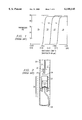
- FIG. 7A is a sketch of a substrate holder 56 which holds an IR transparent substrate 42 such that both sides of 42 are exposed to the MCT vapor in the LPE reactor shown in FIG. 2.
- the rectangular substrate 42 and holder 56 shown is used as a typical example with the understanding that the opening to both 42 sides may be circular, square or any other desired two dimensional geometry and that the holder may be designed for a plurality of substrates rather than just one.
- a cross sectional view of the substrate 42 after it has been exposed to the MCT vapor is shown in FIG. 7B for MCT films 64 and 70 on substrate 42.
- heater 60 is optional and may either supply a constant temperature or graded temperature surface.
- heater 60 is shown as a radiant heater and heater 43 is shown as a conduction heater but the choice is governed by the film properties desired. In this example it is assumed that the average temperature is hotter within film 70 than within film 64. Therefore the Cd interdiffusion from substrate 42 will produce a higher concentration of Cd within zone 68 than 62 directly above it.
- the lateral direction in both MCT films 64 and 70 contain a gradient of decreasing Cd from zone 62 to 66 and zone 68 to 72, respectively.
- the IR properties within zone 68 attenuates or detects shorter wavelengths than the MCT material 62 directly opposite it through IR transparent substrate 42. Through the vertical direction of the two films this results in a narrow band of IR spectrum characteristics with zone 68 attenuating the shorter wavelengths, but passing higher wavelengths to be detected/filtered by zone 62 at only a slightly higher wavelength than zone 68 blocks.
- MCT films 64 and 70 are LPE deposited and heat treated as described in FIG. 7 such that a point lying on MCT film 64 has slightly less Cd than the same lateral location on 70.
- Film 64 is patterned into detectors 86, 88 and 90 (FIG. 8) with attached electrical conductors 80,92 and 82,94 and 84,96 respectively. An increase of conductance in these detectors occurs when irradiated with the proper wavelengths of IR.
- the lateral positions of detectors 86, 88 and 90 determine the center of their IR spectral response.
- the physical widths of detectors 86, 88 and 90 determine their bandwidths.
- the width of detector 86 may detect wavelengths having lower limits from 3 mm on the left to 4.5 mm on the right and the composition of film 70 immediately opposite to detect 86 may pass wavelengths longer than 2.8 mm on the left and 4.3 mm on the right.
- detector 86 may exhibit increases in conductance for only the band of 3 to 4.5 mm.
- Detector 88 has a similarly tailored response at longer wavelengths with a narrower passband than detector 86.
- Detector 90 has a very narrow range of IR wavelength response at a longer wavelength than either detectors 86 or 88 which is desirable when detecting carbon dioxide or carbon monoxide components during combustion of organic material in an atmospheric environment.
- a double sided filter/detector device is that a substantial inventory of double sided film material may be prepared in advance. Subsequently the MCT film 64 may be patterned to achieve an IR response tailored to the application.
- FIG. 9 and Table 5 illustrate two methods of manufacturing active devices and MCT filters and detectors on the same substrate. Although only one MCT film is shown, it should be understood that a plurality of MCT films acting as either or both filters and detectors is possible because the MCT growth temperature of around 450° C. will not harm either unbonded GaAs or unbonded Si devices.
- FIG. 9 illustrates two methods of manufacturing active devices and MCT filters and detectors on the same substrate. Although only one MCT film is shown, it should be understood that a plurality of MCT films acting as either or both filters and detectors is possible because the MCT growth temperature of around 450° C. will not harm either unbonded GaAs or unbonded Si devices.
- GaAs 106 an epitaxially grown film of GaAs 106 is grown on Si substrate 110. Where it is desired to form Si devices in region 112, the GaAs is etched away. Region 112 is fabricated with either or both discrete and integrated Si devices and then covered with a protective layer, such as plasma deposited silicon nitride (not shown) while GaAs devices are created in the GaAs region 108. Both 106 and 110 are covered
- MCT 100 may now be fabricated into detectors having the desired IR wavelength response without harm to the protected circuits 108 and 112.
- the protective layer 104 may now be selectively removed and interconnecting bonding pads opened such that leads may be attached or deposited between 100, 108 and 112 for the final system configuration.
- FIG. 9B shows a similar configuration where only Si devices are required.
- the Si substrate 110 has silicon devices fabricated in region 112 as before and then covered overall with a protective layer of plasma deposited silicon nitride 104.
- the exposed area of Si 110 matches the lattice parameters of ZnSe close enough to allow the epitaxial growth of ZnSe film 114.
- ZnSe also matches the lattice parameters of CdTe close enough to allow the epitaxial growth of CdTe film 102.
- the MCT detector/filter film 100 is grown on 102 and patterned into the desired detector/filter geometries.
- Layer 104 may be selectively removed to expose the bonding pads of 112 and the such that interconnection leads may be bonded between the Si devices of 112 and the detectors formed from 100.
- FIG. 9c shows an integrated device with HgCdTe filter, HgCdTe IR sensors, and silicon circuitry, which can be used, e.g., as a integrated spectrometer.
- Layer 104 has been selectively removed to form a via to expose the bonding pads of 112.
- the MCT film 100 (see FIG. 9b) has been patterned (e.g. photolithographically etched) to form MCT detector stripes 101, 121.
- Via conductor 116 has been formed (e.g. from a metal such as aluminum) in the via and interconnection lead 118 has been used to connect sensor 121 to via conductor 116, thus connecting the Si devices of 112 and the detectors formed from 100.
- Interconnection lead 118 may be from a metal such as aluminum, but is preferably HgTe, and lead 118 is patterned to cover only a small end portion of sensor 121 and to leave most of the sensor uncovered.
- a second lead (not shown) can be used to make a second contact at the opposite end of sensor 121.
- CdTe insulator 120 has been LPE grown between and over the stripes and MCT filter film 122 LPE grown over the CdTe insulator.
- FIG. 9d shows an alternate embodiment in which non-uniform MCT filter film 122 is fabricated using a mask 124 and conventional rapid thermal annealing lamps 126.
- This embodiment can be used in controlled atmosphere containing Hg vapor.
- the mask contains large openings 128 to provide hotter portions of MCT filter film 122, small openings 130, to provide intermediate temperature portions of MCT filter film 122, and solid portions 132 to provide cooler portions of MCT filter film 122.
- a non-contact mask is utilized, and the lamp-mask spacing is not to scale, as the lamps are generally much further away than shown.
- While rapid thermal annealing lamps have previously been used to provide uniform heating, here the lamps are used in conjunction with a reflective mask to provide non-uniform heating. Note that while the mask is shown with holes, it could also be a patterned reflective coating on a transparent substrate. Note also such lamps can also be used in conjunction with a mask to provide non-uniform heating to MCT film 100 (see FIG. 9b) prior to the application of CdTe insulator 120, either before or after film 100 has been patterned to form MCT detector stripes (stripes 101, 121 as shown in FIG. 9c). Such non-uniform heating of film 100 or stripes 101, 121 can provide for MCT detectors having different spectral responses.
- FIG. 9e shows and alternate embodiment in which a controlled atmosphere containing Hg vapor is not used. Instead, the structure of FIG. 9c has been modified by adding a HgTe layer 134 over the MCT filter film 122. Again, non-uniform MCT filter film 122 is fabricated using mask 124 and conventional rapid thermal annealing lamps 126. Generally the HgTe layer is removed after the heating.
- This embodiment can be used to provide an integrated IR detector assembly with a continuously graded HgCdTe filter layer without the use of a controlled atmosphere containing Hg vapor.
- Non-uniform heating could e.g., also be provided by a scanning laser.
- Various modifications and combinations of the illustrative embodiments, as well as other embodiments of the invention, will be apparent to persons skilled in the art upon reference to the description. It is therefore intended that the appended claims encompass any such modifications or embodiments.
Landscapes
- Light Receiving Elements (AREA)
- Radiation Pyrometers (AREA)
Abstract
Description
              TABLE 1
______________________________________
ID#  Description  Function
______________________________________
20   Process chamber
                  Seals process environment
  21 Substrate and holder Supports and rotates substrate for uniform
                    support film deposition.
  22 Substrate holder Supports substrate during deposition
  23 CdTe or CdZnTe Provides surface for epitaxially growing
   substrate MCT.
  24 Stirrer Agitates HgCdTe melt 27 for controlled
    deposition on substrate 23
  25 Hg, Cd, Te vapor Provides Hg vapor rich environment during
    growth of MCT film.
  26 Crucible Container for melt 27
  27 Melt Molten HgCdTe source for MCT film
    deposition.
  28 Chamber Heater Controls temperature of upper process
    chamber.
  29 Thermocouple well Monitors temperature of chamber heater
    28.
______________________________________
              TABLE 2
______________________________________
ID#  Description      Function
______________________________________
39   Zone of 40 having highest
                      Provides shortest IR wavelength
   Cd response
  40 Uniformly deposited MCT Controls range of IR response
   film desired
  41 Zone of 40 having lowest Cd Provides longest IR wavelength
    response
  42 CdTe or CdZnTe substrate Provides a substrate with suitable
    lattice match to MCT for epitaxial
    growth and is transparent to the
    range of IR wavelengths desired.
  43 Heater Provides controlled temperature
    gradient
  44 Hotter portions of heater 43 Interdiffuses more Cd per unit time
                         into zone 40
  45 Cooler portion of heater 43 Interdiffuses less Cd per unit time
                         into zone 40
______________________________________
              TABLE 3
______________________________________
ID#  Description      Function
______________________________________
60   Radiant heater   Provides control over difference of
    annealing temperatures between
    substrate surfaces.
  62 Hotter zone of MCT film 64 Results in higher Cd concentration
                         than zone 66 but less than 68.
  64 MCT film of uniform Determines physical properties
   composition before heat treatment.
  66 Cooler zone of MCT film 64 Results in lower Cd concentration
                         than  zone  62 and 72.
  68 Hotter zone within MCT Results in the highest Cd
   film 70 concentration of any zone in either
    64 or 70.
  70 Same as MCT film 64 on
   the other side of the
   substrate 42.
  72 Cooler zone than 68 but Results in Cd concentration lower
   hotter than zone 66. than zone 68 but higher than 66.
______________________________________
                                  TABLE 4
__________________________________________________________________________
ID# Description      Function
__________________________________________________________________________
42  CdTe or CdZnTe substrate
                     Provide a substrate with suitable lattice match to
                        MCT for epitaxial growth and be transparent to
                        the range of IR wavelengths desired.
  64 Heat treated MCT film as described in Achieve IR response related to
                     MCT film 70.
   FIG. 7B
  68 Highest Cd composition of 70. Attenuate lower and pass higher
                     wavelengths of
    IR spectrum.
  70 Heat treated MCT film as described in Achieve IR response related to
                     MCT film 68.
   FIG. 7B
  72 Lowest Cd composition of 70. Attenuate longer IR wavelengths but
                     pass those
    which will be detected immediately above by
    detector 90.
  86 Detectors; Patterned portions of film 64
    Form wideband IR detector for shorter IR
    wavelengths.
  80, Electrical contacts to detector 86 Forms electrical connection for
                     external
  92, 93  electronics to detect changes of conductance of 86
    with IR radiation.
  88 Patterned portion of film 64 Form medium bandwidth IR detector at
                     medium
    wavelengths of IR spectrum.
  82,94, Electrical contacts to detector 88 Forms electrical connection
                     for external
  95  electronics to detect changes of conductance of 88
    with IR radiation.
  90 Patterned portion of film 64 Form very narrow bandwidth, long
                     wavelength IR
    detector.
  84,96, Electrical contacts to detector 90 Forms electrical connection
                     for external
  97  electronics to detect changes of conductance of 90
    with IR radiation.
  98 Incident IR radiation
__________________________________________________________________________
TABLE 5 ______________________________________ ID# Description Function ______________________________________ 100 MCT film layer To be patterned intoIR detectors 102 CdTe film layer Lattice match between 100 and 106 permits LPE film growth. 104 Plasma deposited silicon Prevents damage toregions 108 nitride or silicon oxide and 112 which contain active protective layer semiconductor devices. 106 GaAs epitaxial layer Can be epitaxially grown on Si and can also provide useful devices within 108. 108 Protected GaAs device May contain discrete or integrated region circuit devices of GaAs. 110 Silicon substrate Provides mechanical support for all epitaxially grown layers and may provideregion 112. 112 Protected Si device region May contain discrete or integrated circuit devices of Si. 114 ZnSe epitaxial layer Provides lattice parameters which allows it to be epitaxially grown on Si and also allows CdTe to be epitaxially grown on it. ______________________________________
Claims (10)
Priority Applications (1)
| Application Number | Priority Date | Filing Date | Title |
|---|---|---|---|
| US09/291,680 US6140145A (en) | 1996-04-04 | 1999-04-13 | Integrated infrared detection system |
Applications Claiming Priority (3)
| Application Number | Priority Date | Filing Date | Title |
|---|---|---|---|
| US1484496P | 1996-04-04 | 1996-04-04 | |
| US08/831,815 US6091127A (en) | 1997-04-02 | 1997-04-02 | Integrated infrared detection system |
| US09/291,680 US6140145A (en) | 1996-04-04 | 1999-04-13 | Integrated infrared detection system |
Related Parent Applications (1)
| Application Number | Title | Priority Date | Filing Date |
|---|---|---|---|
| US08/831,815 Division US6091127A (en) | 1996-04-04 | 1997-04-02 | Integrated infrared detection system |
Publications (1)
| Publication Number | Publication Date |
|---|---|
| US6140145A true US6140145A (en) | 2000-10-31 |
Family
ID=25259932
Family Applications (2)
| Application Number | Title | Priority Date | Filing Date |
|---|---|---|---|
| US08/831,815 Expired - Lifetime US6091127A (en) | 1996-04-04 | 1997-04-02 | Integrated infrared detection system |
| US09/291,680 Expired - Lifetime US6140145A (en) | 1996-04-04 | 1999-04-13 | Integrated infrared detection system |
Family Applications Before (1)
| Application Number | Title | Priority Date | Filing Date |
|---|---|---|---|
| US08/831,815 Expired - Lifetime US6091127A (en) | 1996-04-04 | 1997-04-02 | Integrated infrared detection system |
Country Status (1)
| Country | Link |
|---|---|
| US (2) | US6091127A (en) |
Cited By (2)
| Publication number | Priority date | Publication date | Assignee | Title |
|---|---|---|---|---|
| FR2894074A1 (en) * | 2005-11-30 | 2007-06-01 | Commissariat Energie Atomique | INFRARED SPECTROMETER |
| CN100443928C (en) * | 2006-10-13 | 2008-12-17 | 中国科学院上海技术物理研究所 | Microfilter placed inside the HgCdTe infrared focal plane detector chip |
Families Citing this family (9)
| Publication number | Priority date | Publication date | Assignee | Title |
|---|---|---|---|---|
| EP1328975B1 (en) * | 2000-10-19 | 2011-04-27 | Quantum Semiconductor, LLC | Method of fabricating heterojunction photodiodes integrated with cmos |
| US7265006B2 (en) * | 2000-10-19 | 2007-09-04 | Quantum Semiconductor Llc | Method of fabricating heterojunction devices integrated with CMOS |
| US6828642B2 (en) | 2001-04-17 | 2004-12-07 | Lockhead Martin Corporation | Diffraction grating coupled infrared photodetector |
| US8816443B2 (en) * | 2001-10-12 | 2014-08-26 | Quantum Semiconductor Llc | Method of fabricating heterojunction photodiodes with CMOS |
| US7041983B2 (en) * | 2001-10-12 | 2006-05-09 | Lockheed Martin Corporation | Planar geometry buried junction infrared detector and focal plane array |
| US20060014334A1 (en) * | 2001-10-12 | 2006-01-19 | J R P Augusto Carlos | Method of fabricating heterojunction devices integrated with CMOS |
| US8441018B2 (en) | 2007-08-16 | 2013-05-14 | The Trustees Of Columbia University In The City Of New York | Direct bandgap substrates and methods of making and using |
| CN104597543A (en) * | 2014-12-07 | 2015-05-06 | 杭州麦乐克电子科技有限公司 | 7600 nm long-wave pass infrared filtering sensitive element |
| CN115708226A (en) * | 2021-08-18 | 2023-02-21 | 浙江珏芯微电子有限公司 | Multicolor refrigeration infrared detector and preparation method thereof |
Citations (11)
| Publication number | Priority date | Publication date | Assignee | Title |
|---|---|---|---|---|
| US4376663A (en) * | 1980-11-18 | 1983-03-15 | The United States Of America As Represented By The Secretary Of The Army | Method for growing an epitaxial layer of CdTe on an epitaxial layer of HgCdTe grown on a CdTe substrate |
| JPH01187990A (en) * | 1988-01-22 | 1989-07-27 | Mitsubishi Electric Corp | Manufacture of semiconductor laser device |
| US5367166A (en) * | 1992-03-18 | 1994-11-22 | Philips Electronics Uk Limited | Infrared detector devices and their manufacture |
| US5399503A (en) * | 1989-07-19 | 1995-03-21 | Fujitsu Limited | Method for growing a HgCdTe epitaxial layer on a semiconductor substrate |
| US5449927A (en) * | 1994-05-16 | 1995-09-12 | Santa Barbara Research Center | Multilayer buffer structure including II-VI compounds on a silicon substrate |
| US5581117A (en) * | 1994-12-13 | 1996-12-03 | Nec Corporation | Si base substrate covered by a CdTe or Cd-rich CdZnTe layer |
| US5828068A (en) * | 1996-04-04 | 1998-10-27 | Raytheon Ti Systems, Inc. | Uncooled mercury cadmium telluride infrared devices with integral optical elements |
| US5861626A (en) * | 1996-04-04 | 1999-01-19 | Raytheon Ti System, Inc. | Mercury cadmium telluride infrared filters and detectors and methods of fabrication |
| US5920071A (en) * | 1996-04-04 | 1999-07-06 | Raytheon Company | Mercury cadmium telluride devices for detecting and controlling open flames |
| US5959299A (en) * | 1996-04-04 | 1999-09-28 | Raytheon Company | Uncooled infrared sensors for the detection and identification of chemical products of combustion |
| US6036770A (en) * | 1996-04-04 | 2000-03-14 | Raytheon Company | Method of fabricating a laterally continuously graded mercury cadmium telluride layer |
Family Cites Families (21)
| Publication number | Priority date | Publication date | Assignee | Title |
|---|---|---|---|---|
| US4296324A (en) * | 1979-11-02 | 1981-10-20 | Santa Barbara Research Center | Dual spectrum infrared fire sensor |
| US4370557A (en) * | 1980-08-27 | 1983-01-25 | Honeywell Inc. | Dual detector flame sensor |
| US4769775A (en) * | 1981-05-21 | 1988-09-06 | Santa Barbara Research Center | Microprocessor-controlled fire sensor |
| US4376659A (en) * | 1981-06-01 | 1983-03-15 | Texas Instruments Incorporated | Process for forming semiconductor alloys having a desired bandgap |
| US4607272A (en) * | 1983-10-06 | 1986-08-19 | The United States Of America As Represented By The United States Department Of Energy | Electro-optical SLS devices for operating at new wavelength ranges |
| US4691196A (en) * | 1984-03-23 | 1987-09-01 | Santa Barbara Research Center | Dual spectrum frequency responding fire sensor |
| US4639756A (en) * | 1986-05-05 | 1987-01-27 | Santa Barbara Research Center | Graded gap inversion layer photodiode array |
| US4965649A (en) * | 1988-12-23 | 1990-10-23 | Ford Aerospace Corporation | Manufacture of monolithic infrared focal plane arrays |
| US5479018A (en) * | 1989-05-08 | 1995-12-26 | Westinghouse Electric Corp. | Back surface illuminated infrared detector |
| US5049962A (en) * | 1990-03-07 | 1991-09-17 | Santa Barbara Research Center | Control of optical crosstalk between adjacent photodetecting regions |
| GB2247985A (en) * | 1990-09-12 | 1992-03-18 | Philips Electronic Associated | Plural-wavelength infrared detector devices |
| US5459321A (en) * | 1990-12-26 | 1995-10-17 | The United States Of America As Represented By The Secretary Of The Navy | Laser hardened backside illuminated optical detector |
| US5192695A (en) * | 1991-07-09 | 1993-03-09 | Fermionics Corporation | Method of making an infrared detector |
| JP3263964B2 (en) * | 1992-01-31 | 2002-03-11 | 富士通株式会社 | Crystal for forming semiconductor device and manufacturing method thereof |
| US5510644A (en) * | 1992-03-23 | 1996-04-23 | Martin Marietta Corporation | CDTE x-ray detector for use at room temperature |
| US5373182A (en) * | 1993-01-12 | 1994-12-13 | Santa Barbara Research Center | Integrated IR and visible detector |
| US5380669A (en) * | 1993-02-08 | 1995-01-10 | Santa Barbara Research Center | Method of fabricating a two-color detector using LPE crystal growth |
| US5457331A (en) * | 1993-04-08 | 1995-10-10 | Santa Barbara Research Center | Dual-band infrared radiation detector optimized for fabrication in compositionally graded HgCdTe |
| US5391882A (en) * | 1993-06-11 | 1995-02-21 | Santa Barbara Research Center | Semiconductor gamma ray detector including compositionally graded, leakage current blocking potential barrier layers and method of fabricating the detector |
| US5559336A (en) * | 1994-07-05 | 1996-09-24 | Santa Barbara Research Center | Integrated LPE-grown structure for simultaneous detection of infrared radiation in two bands |
| US5633527A (en) * | 1995-02-06 | 1997-05-27 | Sandia Corporation | Unitary lens semiconductor device |
-
1997
- 1997-04-02 US US08/831,815 patent/US6091127A/en not_active Expired - Lifetime
-
1999
- 1999-04-13 US US09/291,680 patent/US6140145A/en not_active Expired - Lifetime
Patent Citations (11)
| Publication number | Priority date | Publication date | Assignee | Title |
|---|---|---|---|---|
| US4376663A (en) * | 1980-11-18 | 1983-03-15 | The United States Of America As Represented By The Secretary Of The Army | Method for growing an epitaxial layer of CdTe on an epitaxial layer of HgCdTe grown on a CdTe substrate |
| JPH01187990A (en) * | 1988-01-22 | 1989-07-27 | Mitsubishi Electric Corp | Manufacture of semiconductor laser device |
| US5399503A (en) * | 1989-07-19 | 1995-03-21 | Fujitsu Limited | Method for growing a HgCdTe epitaxial layer on a semiconductor substrate |
| US5367166A (en) * | 1992-03-18 | 1994-11-22 | Philips Electronics Uk Limited | Infrared detector devices and their manufacture |
| US5449927A (en) * | 1994-05-16 | 1995-09-12 | Santa Barbara Research Center | Multilayer buffer structure including II-VI compounds on a silicon substrate |
| US5581117A (en) * | 1994-12-13 | 1996-12-03 | Nec Corporation | Si base substrate covered by a CdTe or Cd-rich CdZnTe layer |
| US5828068A (en) * | 1996-04-04 | 1998-10-27 | Raytheon Ti Systems, Inc. | Uncooled mercury cadmium telluride infrared devices with integral optical elements |
| US5861626A (en) * | 1996-04-04 | 1999-01-19 | Raytheon Ti System, Inc. | Mercury cadmium telluride infrared filters and detectors and methods of fabrication |
| US5920071A (en) * | 1996-04-04 | 1999-07-06 | Raytheon Company | Mercury cadmium telluride devices for detecting and controlling open flames |
| US5959299A (en) * | 1996-04-04 | 1999-09-28 | Raytheon Company | Uncooled infrared sensors for the detection and identification of chemical products of combustion |
| US6036770A (en) * | 1996-04-04 | 2000-03-14 | Raytheon Company | Method of fabricating a laterally continuously graded mercury cadmium telluride layer |
Cited By (2)
| Publication number | Priority date | Publication date | Assignee | Title |
|---|---|---|---|---|
| FR2894074A1 (en) * | 2005-11-30 | 2007-06-01 | Commissariat Energie Atomique | INFRARED SPECTROMETER |
| CN100443928C (en) * | 2006-10-13 | 2008-12-17 | 中国科学院上海技术物理研究所 | Microfilter placed inside the HgCdTe infrared focal plane detector chip |
Also Published As
| Publication number | Publication date |
|---|---|
| US6091127A (en) | 2000-07-18 |
Similar Documents
| Publication | Publication Date | Title |
|---|---|---|
| US5861626A (en) | Mercury cadmium telluride infrared filters and detectors and methods of fabrication | |
| US6140145A (en) | Integrated infrared detection system | |
| US6770882B2 (en) | Micromachined pyro-optical structure | |
| KR0135119B1 (en) | Infrared detector | |
| US6392232B1 (en) | High fill factor bolometer array | |
| US5021663A (en) | Infrared detector | |
| US5777328A (en) | Ramped foot support | |
| US5288649A (en) | Method for forming uncooled infrared detector | |
| US5861545A (en) | Micromachined inferential opto-thermal gas sensor | |
| JP4054069B2 (en) | Photothermal gas sensor manufactured by micromachining method | |
| US5689087A (en) | Integrated thermopile sensor for automotive, spectroscopic and imaging applications, and methods of fabricating same | |
| US5789753A (en) | Stress tolerant bolometer | |
| US20070034978A1 (en) | Photonic crystal emitter, detector and sensor | |
| US6998613B2 (en) | Integrated spectroscopic microbolometer with microfilter arrays | |
| Iborra et al. | IR uncooled bolometers based on amorphous Ge/sub x/Si/sub 1-x/O/sub y/on silicon micromachined structures | |
| EP0534768A1 (en) | Uncooled infrared detector and method for forming the same | |
| CA2242293A1 (en) | Passive infrared analysis gas sensors and applicable multichannel detector assemblies | |
| US5406081A (en) | Infrared detector utilizing diamond film | |
| US6036770A (en) | Method of fabricating a laterally continuously graded mercury cadmium telluride layer | |
| JPS6021960B2 (en) | Manufacturing method of Hg↓1-↓xCd↓xTe composition layer | |
| JPH04230073A (en) | Photosensitive element array and its manufacture | |
| US6198099B1 (en) | Bolometer including a reflective layer | |
| US5959299A (en) | Uncooled infrared sensors for the detection and identification of chemical products of combustion | |
| US5920071A (en) | Mercury cadmium telluride devices for detecting and controlling open flames | |
| US5828068A (en) | Uncooled mercury cadmium telluride infrared devices with integral optical elements |
Legal Events
| Date | Code | Title | Description |
|---|---|---|---|
| STCF | Information on status: patent grant |
Free format text: PATENTED CASE |
|
| CC | Certificate of correction | ||
| FEPP | Fee payment procedure |
Free format text: PAYOR NUMBER ASSIGNED (ORIGINAL EVENT CODE: ASPN); ENTITY STATUS OF PATENT OWNER: LARGE ENTITY |
|
| FPAY | Fee payment |
Year of fee payment: 4 |
|
| FPAY | Fee payment |
Year of fee payment: 8 |
|
| FPAY | Fee payment |
Year of fee payment: 12 |
|
| AS | Assignment |
Owner name: OL SECURITY LIMITED LIABILITY COMPANY, DELAWARE Free format text: ASSIGNMENT OF ASSIGNORS INTEREST;ASSIGNOR:RAYTHEON COMPANY;REEL/FRAME:029117/0335 Effective date: 20120730 |
|
| FEPP | Fee payment procedure |
Free format text: PAYER NUMBER DE-ASSIGNED (ORIGINAL EVENT CODE: RMPN); ENTITY STATUS OF PATENT OWNER: LARGE ENTITY Free format text: PAYOR NUMBER ASSIGNED (ORIGINAL EVENT CODE: ASPN); ENTITY STATUS OF PATENT OWNER: LARGE ENTITY |
|
| AS | Assignment |
Owner name: HANGER SOLUTIONS, LLC, GEORGIA Free format text: ASSIGNMENT OF ASSIGNORS INTEREST;ASSIGNOR:INTELLECTUAL VENTURES ASSETS 158 LLC;REEL/FRAME:051486/0425 Effective date: 20191206 |
|
| AS | Assignment |
Owner name: INTELLECTUAL VENTURES ASSETS 158 LLC, DELAWARE Free format text: ASSIGNMENT OF ASSIGNORS INTEREST;ASSIGNOR:OL SECURITY LIMITED LIABILITY COMPANY;REEL/FRAME:051846/0192 Effective date: 20191126 |