US6120328A - Thin smart card connector - Google Patents
Thin smart card connector Download PDFInfo
- Publication number
- US6120328A US6120328A US09/503,756 US50375600A US6120328A US 6120328 A US6120328 A US 6120328A US 50375600 A US50375600 A US 50375600A US 6120328 A US6120328 A US 6120328A
- Authority
- US
- United States
- Prior art keywords
- circuit board
- contact
- card
- trace
- lying
- Prior art date
- Legal status (The legal status is an assumption and is not a legal conclusion. Google has not performed a legal analysis and makes no representation as to the accuracy of the status listed.)
- Expired - Fee Related
Links
Images


Classifications
-
- H—ELECTRICITY
- H01—ELECTRIC ELEMENTS
- H01R—ELECTRICALLY-CONDUCTIVE CONNECTIONS; STRUCTURAL ASSOCIATIONS OF A PLURALITY OF MUTUALLY-INSULATED ELECTRICAL CONNECTING ELEMENTS; COUPLING DEVICES; CURRENT COLLECTORS
- H01R13/00—Details of coupling devices of the kinds covered by groups H01R12/70 or H01R24/00 - H01R33/00
- H01R13/02—Contact members
- H01R13/22—Contacts for co-operating by abutting
- H01R13/24—Contacts for co-operating by abutting resilient; resiliently-mounted
- H01R13/2442—Contacts for co-operating by abutting resilient; resiliently-mounted with a single cantilevered beam
-
- G—PHYSICS
- G06—COMPUTING; CALCULATING OR COUNTING
- G06K—GRAPHICAL DATA READING; PRESENTATION OF DATA; RECORD CARRIERS; HANDLING RECORD CARRIERS
- G06K7/00—Methods or arrangements for sensing record carriers, e.g. for reading patterns
- G06K7/0013—Methods or arrangements for sensing record carriers, e.g. for reading patterns by galvanic contacts, e.g. card connectors for ISO-7816 compliant smart cards or memory cards, e.g. SD card readers
- G06K7/0021—Methods or arrangements for sensing record carriers, e.g. for reading patterns by galvanic contacts, e.g. card connectors for ISO-7816 compliant smart cards or memory cards, e.g. SD card readers for reading/sensing record carriers having surface contacts
-
- H—ELECTRICITY
- H01—ELECTRIC ELEMENTS
- H01R—ELECTRICALLY-CONDUCTIVE CONNECTIONS; STRUCTURAL ASSOCIATIONS OF A PLURALITY OF MUTUALLY-INSULATED ELECTRICAL CONNECTING ELEMENTS; COUPLING DEVICES; CURRENT COLLECTORS
- H01R13/00—Details of coupling devices of the kinds covered by groups H01R12/70 or H01R24/00 - H01R33/00
- H01R13/02—Contact members
- H01R13/22—Contacts for co-operating by abutting
- H01R13/24—Contacts for co-operating by abutting resilient; resiliently-mounted
- H01R13/245—Contacts for co-operating by abutting resilient; resiliently-mounted by stamped-out resilient contact arm
-
- H—ELECTRICITY
- H01—ELECTRIC ELEMENTS
- H01R—ELECTRICALLY-CONDUCTIVE CONNECTIONS; STRUCTURAL ASSOCIATIONS OF A PLURALITY OF MUTUALLY-INSULATED ELECTRICAL CONNECTING ELEMENTS; COUPLING DEVICES; CURRENT COLLECTORS
- H01R13/00—Details of coupling devices of the kinds covered by groups H01R12/70 or H01R24/00 - H01R33/00
- H01R13/40—Securing contact members in or to a base or case; Insulating of contact members
- H01R13/405—Securing in non-demountable manner, e.g. moulding, riveting
- H01R13/41—Securing in non-demountable manner, e.g. moulding, riveting by frictional grip in grommet, panel or base
-
- H—ELECTRICITY
- H01—ELECTRIC ELEMENTS
- H01R—ELECTRICALLY-CONDUCTIVE CONNECTIONS; STRUCTURAL ASSOCIATIONS OF A PLURALITY OF MUTUALLY-INSULATED ELECTRICAL CONNECTING ELEMENTS; COUPLING DEVICES; CURRENT COLLECTORS
- H01R2201/00—Connectors or connections adapted for particular applications
- H01R2201/16—Connectors or connections adapted for particular applications for telephony
Definitions
- a smart card reader commonly includes a circuit board, a support plate mounted on the circuit board, and contacts mounted on the support plate and engaging electrically conductive traces on the circuit board.
- the contacts have blades that project above the plate to engage the contact pads of the smart card, and have connection ends that are soldered to the traces on the circuit board.
- a smart card electrical connector which is of small thickness while providing secure mounting of the contacts.
- the connector includes an insulative support plate for lying on a circuit board and contacts mounted on the support plate, with each contact having a blade that projects at an upward incline above the upper face of the support, and having a rear portion for mounting on the support plate.
- the contact rear portion includes a mount part that lies in a downwardly-facing recess of the support plate, and a pair of retainers on laterally opposite sides of the mount part.
- the retainers have ears that lie in a higher plane than the mount portion and that lie in upwardly-facing recesses in the support plate.
- Each retention tab preferably has front and rear ears that each lies in a recess of the support plate.
- At least one of the recesses forms a rearwardly-facing shoulder and at least one of the recesses forms a forwardly-facing shoulder, to prevent forward-rearward movement of the contact.
- One of the shoulders such as the forwardly-facing shoulder, can be formed at the front end of an inclined surface to enable the contact to snap into place.
- the ears can lie at the ends of elongated beams, so the ears can be deflected together to prevent "rattling" of the contact.
- One of the contacts can include a switching contact which includes a pair of laterally spaced blades and a switch beam that lies between the blades.
- the switch beam has a first end that is coupled to the blades to be depressed when the blades are depressed, and the switch beam has a free second end.
- the blades When the blades are depressed by a card, they cause the switch beam to be depressed until its free second end engages a conductive trace on the circuit board, without the card directly engaging the switch beam.
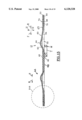
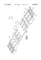
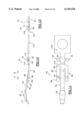
- FIG. 1 is an isometric top view of a connector of the present invention.
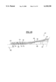
- FIG. 2 is an isometric bottom view of the connector of FIG. 1.
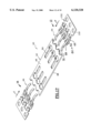
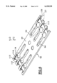
- FIG. 3 is an exploded isometric view of the components of the connector of FIG. 1.
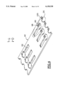
- FIG. 4 is a top isometric view of the support plate of the connector of FIG. 1.
- FIG. 5 is an enlarged view of the area D5 of FIG. 4.
- FIG. 6 is a bottom isometric view of the support plate of FIG. 1.
- FIG. 7 is an enlarged view of the area D7 of FIG. 6.
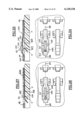
- FIG. 8 is an isometric rear view of a contact of the connector of FIG. 1.
- FIG. 9 is an isometric bottom view of the contact of FIG. 8.
- FIG. 10 is a side elevation view of the contact of FIG. 8, but before the contact is cut from a larger sheet of metal.
- FIG. 11 is a top view of the contact of FIG. 10.
- FIG. 12 is a front end view of the contact of FIG. 10.
- FIG. 13 is a sectional view of a portion of the connector of FIG. 1, showing the retaining tabs.
- FIG. 14 is an enlarged view of the area D14 of FIG. 13.
- FIG. 15 is a sectional view of a portion of the connector of FIG. 1.
- FIG. 16 is an enlarged view of the area D16 of FIG. 15.
- FIG. 17 is an exploded isometric view similar to that of FIG. 3, but showing a manufactured metal sheet from which the contacts are cut.
- FIG. 18 is an isometric top view of a second embodiment of the invention, which includes a switching contact for detecting the presence of a card.
- FIG. 19 is an enlarged view of the area D19 in FIG. 18.
- FIG. 20 is an isometric view of one of the switching contacts of the connector of FIG. 18.
- FIG. 21 is a side view of the contact of FIG. 20.
- FIG. 22 is a top view of the contact of FIG. 20.
- FIG. 23 is a front elevation view of the contact of FIG. 22.
- FIG. 24 is a partial top view of the connector of FIG. 18 with a switching contact in the rest, or open position.
- FIG. 25 is a sectional view taken on line 25--25 of FIG. 24.
- FIG. 26 is a view similar to that of FIG. 24, but with the switching contact in a closed position.
- FIG. 27 is a view taken on line 27--27 of FIG. 26, and which is similar to FIG. 25 except that the switching contact is in a closed position.
- FIG. 28 is an isometric bottom view of the circuit board of FIG. 18.
- FIG. 29 is an enlarged view of the area D29 of FIG. 28.
- FIG. 30 is a top view of the circuit board of FIG. 28.
- FIG. 31 is an isometric top view of the support plate of the connector of FIG. 18.
- FIG. 32 is a top rear isometric view of a switching contact constructed in accordance with another embodiment of the invention.
- FIG. 33 is a side elevation view of the switching contact of FIG. 32.
- FIG. 34 is a plan view of the switching contact of FIG. 33.
- FIG. 35 is a front elevation view of the contact of FIG. 34.
- FIG. 36 is a sectional side view showing the contact of FIG. 33 in a fully closed position, and showing the support plate and a circuit board.
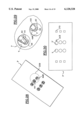
- FIG. 1 illustrates an electrical connector 40 which includes an insulative support plate 42 and a plurality of electrical contacts 44.
- the support plate is mounted on a circuit board 16, with connection ends 68 of the contacts soldered to traces on the circuit board.
- a smart card C with contact pads B is inserted in a longitudinal direction M over an upper face 46 of the insulative support, with the contact pads engaging blades 60 of the contacts when the card is in its fully installed position.
- a card guide 18 engages laterally L opposite sides of the card to guide it along its path of sliding to its final position. It is also possible for the card to be moved downward D to its final position. An opposite upward direction is indicated by arrow U.
- the contacts are arranged in two rows 12, 14, with the contacts in one row being turned 180 degrees about a vertical axis with respect to the contacts of the other row.
- applicant defines forward and rearward directions F, R for each row, with the contact blades 60 lying at the front of each contact and with each contact having a rear portion 61 where the contact is mounted.
- the support plate 42 is of substantially rectangular shape, with longitudinally opposite lateral edges 50 and laterally opposite edges 49.
- the support plate 42 has upper and lower faces 46, 48.
- each contact 44 includes the resiliently deflectable contact blade 60 and the contact rear portion 61.
- the contact blade has a free front end 62 with a convexly curved upper face and which has a contact location 22 where the contact engages a smart card pad.
- the blade has a part 64 that extends to a blade rear end 63 that merges with the contact rear portion 61.
- the contact rear portion includes a mount part 66 that lies directly rearward of the blade 60 and a pair of retainers 80 lying at laterally opposite sides of the mount part 66 and connected thereto by lateral joiner parts 24. It is noted that the contact has a vertical center plane of symmetry 75 that extends along the contact blade 60 and through the middle of the mount part 66, with the retainers 80 lying on laterally opposite sides of the center plane.
- Each of the retainers 80 includes front and rear branches 82, 84.
- the front branch 82 includes a longitudinally extending beam 26 that extends forwardly from a joiner part 24, and an ear 104 that is bent to lie higher than the mount part 66.
- Each of the rear branches 84 also includes an ear 118 that is bent to extend in a plane that is higher than the plane of the mount portion 66.
- Each ear 118 has a raised lower surface 132 and a side edge 140.
- the mount portion 66 lies in a downwardly-opening recess in the support plate, while the ears 104, 118 lie in upwardly-opening recesses in the support plate.
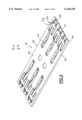
- FIG. 5 shows a portion of the support plate 42.
- the support plate has a longitudinally-extending slot 52 with a rear portion 90 having a cutout 58, through which the contact blade extends.
- the support plate has a downwardly-opening cavity or recess 70, and has four upwardly-opening recesses 98, 120. Walls 126 forming the recesses 120, have upper surfaces 124.
- the mount part 66 of the contact of FIG. 8 lies in the downwardly-opening recess 70.
- the ears 104, 118 of the contact lie in the upwardly-opening recesses 98, 120.
- FIG. 1 shows how the mount part 66 and ears 104, 118 are mounted in the recesses.
- the mount part 66 prevents upward movement of the contact, while the four ears 104, 118 limit tilt of the contact and its contact blade about any axis.
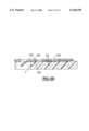
- FIG. 15 shows that the contact blade 60 projects at a forward and upward incline to above the upper face 46 of the support plate 42.
- the mount part 66 which lies in the recess 70, lies under a thin part 72 of the support plate.
- the rear connection end 68 is bent to be very slightly above the mount part 66 to accommodate the thickness of a trace 77 (FIG. 16) on the circuit board to which the surface 76 of the connection end 68 is soldered.
- FIG. 16 shows details for another contact 44 of the connector.
- FIG. 13 shows the front and rear branches 82, 84 of a retainer 80.
- FIG. 14 shows the area in greater detail.
- the front branch 82 lies within the downwardly-opening recess 70 in the support plate, and is joined by an S curve bend 88 to the front ear 104.
- Front ear 104 lies in an upper plane 25 that is higher than the lower plane 27 in which most of the retainer forward branch 82 lies and in which the mount part 66 lies.
- the front branches 82 have beams 26 that are elongated in a longitudinal direction M which allows their ears 104 to be resiliently moved slightly together and apart along a lateral direction L. This allows the ears to be deflected slightly together when they press against side edges 100 (FIG.
- FIG. 8 shows that each forward branch 82 of the retainer forms rearwardly-facing shoulders 110 at its rear.
- the rearwardly-facing shoulders engage forwardly-facing support shoulders 114 (FIG. 7) near the rear of the downwardly-opening recess 70.
- the front ears 104 have forwardly-facing edges 108 which engage rearwardly-facing support shoulders 102 (FIG. 5) at the front of the upwardly-opening recesses 98. This prevents forward and rearward longitudinal movement of the contact within the support plate.
- the shoulders 114 are formed on catches 112 that have downwardly-forwardly inclined bottom surfaces that aid in snapping the contact into position as it is installed so its full installation can be sensed.
- Each rear branch 84 has an S-shaped bend 116 that places the ear 118 at a higher level than the mount portion 66.
- the contact is soldered at the connection end 68 to a trace on the circuit board, the connection end 68 being very slightly raised, as by 0.07 mm, to account for the thickness of the circuit board trace under it.
- a slight bend at 117 allows the slight raising of the connection end.
- each contact blade lies in a downwardly-opening recess 56 of the support plate.
- the contact front end 62 is biased slightly upwardly against a top wall 54 of the front recess 56. This prevents the blade front end 62 from being exposed, and possibly being damaged if an object is slid under it.
- the circuit board 16 of FIG. 15 has holes T into which the front end of the blade can be depressed, to enable the connector to have a very low height above the upper face of the circuit board.
- FIG. 10 shows that the blade front end 62 has a downward-forward inclined part 63 lying forward of the topmost location 65 of the contact blade. The inclined part 63 is received in a circuit board hole.
- the support 42 is preferably molded of insulative or dielectric material. It preferably has a thickness of less than 1 mm, and may have a thickness of about 0.4 mm with its thinnest parts such as 74 having a thickness of about 0.2 mm. In an electrical connector that applicant has designed, the support 42 has a thickness 0.37 mm, with part 74 having a thickness of 0.2 mm and with the contact blade part 66 having a thickness of 0.17 mm. No large stresses are applied to the support plate and therefore it is very stable during high temperature solder reflow operations.
- the support plate has sufficient flexibility to assure that the connector is robust when its contacts are soldered to traces on the circuit board, even when the circuit board is subjected to torsional deformation. The amount of material in the support plate is very small, allowing the use of very high strength polymers which have a high cost per unit mass.
- the contacts 44 are produced by cutting and bending a sheet of electrically conductive material 150 such as a copper alloy.
- a portion 152 of the sheet forms a contact holder for holding each row 12, 14 of contacts together as they are simultaneously inserted into the support plate.
- the portion 152 is then cut from the contacts.
- the three contacts are positioned below the lower face 48 of the support plate 42 so the front ends 86 of the front branches 82 of the retainers 80 lie below the recesses in the support plate.
- the contacts are then raised upwardly to bring the mount parts 66 against the upper wall of the downwardly-extending recesses 70.
- the row of contacts is moved forward until the contacts are snapped into the mounted position, with their ears lying in the upwardly-extending recesses.
- the portions 152 are separated from the contacts.
- FIG. 27 shows the front end 62 of the blades 162 depressed so they are substantially even with the upper face 46 of the support plate 42A
- the front end 158 of the switch beam lies below the level of the front end 62 of the blade 162.
- FIG. 30 shows two traces 163, 170 on the circuit board P, with the rear trace 170 being soldered to the rear of the contact and the front trace 163 lying under the front end of the switch beam. Holes such as T and T' receive the extreme front end of the contact blades.
- FIGS. 32-36 illustrate another switching contact 44B which is similar to that of FIGS. 19-31, except that the switching blade 156B is joined to the front ends of the contact blades 162 instead of the rear end.
- the connector can be used in any orientation with respect to the Earth.
- the connector includes an insulative support plate and at least one contact mounted on the support plate.
- the contact has a card-engaging blade and has a rear portion for mounting the contact.
- the rear portion includes a mount part and a pair of retainers lying on laterally opposite sides of the mount part.
- the retainers have ears lying out of the plane of the mount part.
- the support plate has a first recess opening in a first direction such as the downward direction, which receives the mount part.
- the support plate has a plurality of additional recesses opening in a second direction such as the upward direction, which receives the ears.
- Each retainer preferably has front and rear branches with an ear at each branch, with the ears lying in a higher plane than the mount part and lying in upwardly-facing recesses while the mount part lies in a downwardly-facing recess.
- the front ears abut a rearwardly-facing shoulder of the support plate.
- the front ears lie at the front ends of elongated beams, and are deflected closer together.
- a front branch of each retainer has a rearwardly-facing shoulder that abuts a forwardly-facing shoulder on an inclined catch of the support plate.
- a contact can be a switching contact, which includes a blade that directly engages an inserted card, and a switch beam with one end coupled to the blade to be depressed when the blade is depressed, and with the other end of the switch beam being a free end and being depressable against a switching trace on the circuit board.
- a card does not have to directly depress the switch beam, but needs only depress the contact blade.
Abstract
Description
Claims (6)
Priority Applications (1)
| Application Number | Priority Date | Filing Date | Title |
|---|---|---|---|
| US09/503,756 US6120328A (en) | 1997-12-26 | 2000-02-14 | Thin smart card connector |
Applications Claiming Priority (4)
| Application Number | Priority Date | Filing Date | Title |
|---|---|---|---|
| FR97165565 | 1997-12-26 | ||
| FR9716565A FR2773275B1 (en) | 1997-12-26 | 1997-12-26 | VERY LOW THICKNESS ELECTRICAL CONNECTOR FOR CONNECTION OF AN ELECTRONIC MEMORY CARD |
| US09/218,118 US6053776A (en) | 1997-12-26 | 1998-12-21 | Thin smart card connector |
| US09/503,756 US6120328A (en) | 1997-12-26 | 2000-02-14 | Thin smart card connector |
Related Parent Applications (1)
| Application Number | Title | Priority Date | Filing Date |
|---|---|---|---|
| US09/218,118 Continuation US6053776A (en) | 1997-12-26 | 1998-12-21 | Thin smart card connector |
Publications (1)
| Publication Number | Publication Date |
|---|---|
| US6120328A true US6120328A (en) | 2000-09-19 |
Family
ID=9515185
Family Applications (2)
| Application Number | Title | Priority Date | Filing Date |
|---|---|---|---|
| US09/218,118 Expired - Fee Related US6053776A (en) | 1997-12-26 | 1998-12-21 | Thin smart card connector |
| US09/503,756 Expired - Fee Related US6120328A (en) | 1997-12-26 | 2000-02-14 | Thin smart card connector |
Family Applications Before (1)
| Application Number | Title | Priority Date | Filing Date |
|---|---|---|---|
| US09/218,118 Expired - Fee Related US6053776A (en) | 1997-12-26 | 1998-12-21 | Thin smart card connector |
Country Status (8)
| Country | Link |
|---|---|
| US (2) | US6053776A (en) |
| EP (1) | EP0926769B1 (en) |
| JP (1) | JPH11250965A (en) |
| CN (1) | CN1221237A (en) |
| CA (1) | CA2254226A1 (en) |
| DE (1) | DE69837700T2 (en) |
| FR (1) | FR2773275B1 (en) |
| TW (1) | TW421899B (en) |
Cited By (27)
| Publication number | Priority date | Publication date | Assignee | Title |
|---|---|---|---|---|
| WO2002056419A2 (en) * | 2000-12-21 | 2002-07-18 | Amphenol-Tuchel Electronics Gmbh | A flat contact element for a smart card connector and a smart card connector using a flat contact element |
| US20030060085A1 (en) * | 2001-09-15 | 2003-03-27 | Kenneth Reece | Circuit board IC card connector |
| US6642460B2 (en) | 2002-01-23 | 2003-11-04 | Eaton Corporation | Switch assembly employing an external customizing printed circuit board |
| US20040134840A1 (en) * | 2001-06-12 | 2004-07-15 | Gianfranco Salmi | Method and a station for checking the integrity of packages, in particular single-dose packages |
| US20040152361A1 (en) * | 2003-01-20 | 2004-08-05 | Tsai Chou Hsuan | Electrical card connector having a bevel slot |
| US20040209519A1 (en) * | 2001-09-13 | 2004-10-21 | Hiromasa Yokoyama | Electric connector |
| US20050020137A1 (en) * | 2002-10-30 | 2005-01-27 | Hirohisa Tanaka | Connector and contact for the connector |
| US20050026463A1 (en) * | 2003-08-01 | 2005-02-03 | Harris Shaun L. | Electrical connector |
| US20050124223A1 (en) * | 2003-12-03 | 2005-06-09 | Chi Zhang | Electrical contact |
| US20050130500A1 (en) * | 2000-06-14 | 2005-06-16 | Leland Wang | Compound connector for two different types of electronic packages |
| US6942515B1 (en) * | 2004-11-15 | 2005-09-13 | Yung-Yu Wu | Connector |
| US20050266741A1 (en) * | 2004-05-31 | 2005-12-01 | Japan Aviation Electronics Industry, Limited | Connector which can be reduced in warpage |
| US20060089037A1 (en) * | 2004-10-27 | 2006-04-27 | Japan Aviation Electronics Industry, Limited | Connector apparatus easy in removing operation |
| DE10061533B4 (en) * | 2000-12-11 | 2006-05-04 | Amphenol-Tuchel Electronics Gmbh | Self-supporting contact spring, in particular for a smart card connector |
| US20070042615A1 (en) * | 2005-08-22 | 2007-02-22 | Hon Hai Precision Ind. Co., Ltd. | Land grid array socket |
| US7247062B1 (en) * | 2006-08-28 | 2007-07-24 | Hon Hai Precision Ind. Co., Ltd. | Electrical contact used in an electrical socket |
| US20080038957A1 (en) * | 2006-08-08 | 2008-02-14 | Hon Hai Precision Ind. Co., Ltd. | Electrical connector with improved terminals |
| CN100421310C (en) * | 2004-05-31 | 2008-09-24 | 日本航空电子工业株式会社 | Connector which can be reduced in warpage |
| US20080318445A1 (en) * | 2007-06-19 | 2008-12-25 | Hon Hai Precision Ind. Co., Ltd. | Electrical connector with improved housing |
| US7473126B1 (en) * | 2007-07-10 | 2009-01-06 | Hon Hai Precision Ind. Co., Ltd. | Battery connector with improved contact |
| US20090035995A1 (en) * | 2007-08-03 | 2009-02-05 | Hon Hai Precision Ind. Co., Ltd. | Electrical connector with improved housing structure |
| US20090088030A1 (en) * | 2007-10-01 | 2009-04-02 | Konrad Stromiedel | Conductor terminal |
| US20100098280A1 (en) * | 2006-01-30 | 2010-04-22 | Songbird Hearing, Inc. | Hearing aid |
| US7909657B1 (en) | 2009-11-12 | 2011-03-22 | Hubbell Incorporated | Electrical connector with low-stress, reduced-electrical-length contacts |
| US20130210280A1 (en) * | 2010-05-27 | 2013-08-15 | Molex Incorporated | Electronic card connector |
| CN103259116A (en) * | 2012-02-20 | 2013-08-21 | 莫列斯公司 | Connector |
| US10535949B2 (en) * | 2017-11-15 | 2020-01-14 | Foxconn Interconnect Technology Limited | Electrical connector having complementary configurations of opposite contacts |
Families Citing this family (29)
| Publication number | Priority date | Publication date | Assignee | Title |
|---|---|---|---|---|
| US7120509B1 (en) | 1999-09-17 | 2006-10-10 | Hasbro, Inc. | Sound and image producing system |
| DE10062464B4 (en) * | 1999-12-23 | 2011-03-31 | Zf Friedrichshafen Ag | Electrical plug connection |
| DE60040807D1 (en) * | 2000-02-25 | 2008-12-24 | Hasbro Inc | SOUND AND PICTURE GENERATION SYSTEM |
| FR2809871B1 (en) * | 2000-06-05 | 2002-07-19 | Itt Mfg Entpr S Inc | ELECTRICAL CONNECTOR WITH IMPROVED CONTACT BLADES FOR CONNECTION OF AN INTEGRATED CIRCUIT (S) CARD |
| JP4714964B2 (en) * | 2000-06-30 | 2011-07-06 | ミツミ電機株式会社 | Memory card connector |
| DE10037744A1 (en) * | 2000-08-02 | 2002-02-14 | Siemens Ag | Device with chip card |
| TW474496U (en) * | 2000-12-20 | 2002-01-21 | Hon Hai Prec Ind Co Ltd | Electronic card connector |
| DE10243479A1 (en) * | 2002-09-19 | 2004-03-25 | Neutrik Aktiengesellschaft | Plug contact for electrical plug connections |
| CN2682631Y (en) * | 2003-12-16 | 2005-03-02 | 富士康(昆山)电脑接插件有限公司 | Electronic card connector |
| US7350705B1 (en) | 2005-03-28 | 2008-04-01 | International Technologies & Systems Corp. | Compact robust smart card reader |
| DE102005027213A1 (en) * | 2005-06-13 | 2006-12-14 | Amphenol-Tuchel Electronics Gmbh | Simblock with special contact attachment |
| TWI255077B (en) * | 2005-06-27 | 2006-05-11 | Fci Asia Technology Pte Ltd | Housing, terminal and connector using the housing and the terminal |
| US7361060B2 (en) * | 2005-08-04 | 2008-04-22 | Illinois Tool Works Inc | Connector with bifurcated conductor |
| JP4844927B2 (en) * | 2006-06-02 | 2011-12-28 | Smk株式会社 | Card connector |
| JP5110442B2 (en) * | 2009-03-05 | 2012-12-26 | 山一電機株式会社 | Card connector |
| JP4866459B2 (en) | 2009-12-08 | 2012-02-01 | モレックス インコーポレイテド | Card connector |
| JP5117559B2 (en) * | 2010-11-05 | 2013-01-16 | Smk株式会社 | Memory card connector |
| CN202268512U (en) * | 2011-10-27 | 2012-06-06 | 昆山联滔电子有限公司 | Cable connector |
| DE102012005852B4 (en) * | 2012-03-22 | 2014-02-27 | Amphenol-Tuchel Electronics Gmbh | Switching spring assembly |
| JP5382385B2 (en) * | 2012-03-28 | 2014-01-08 | Smk株式会社 | Card connector |
| CN102957021A (en) * | 2012-12-04 | 2013-03-06 | 张家港华捷电子有限公司 | SIM (Subscriber Identity Module) card connector for mobile phone |
| CN105098415B (en) * | 2014-05-07 | 2017-12-05 | 莫仕连接器(成都)有限公司 | Terminal base and electronic card coupler |
| JP6597393B2 (en) * | 2016-02-29 | 2019-10-30 | 住友電装株式会社 | Resin molded product and its manufacturing method |
| CN107134674B (en) * | 2016-02-29 | 2021-04-27 | 泰科电子(上海)有限公司 | Conductive connecting piece and connecting assembly |
| USD950498S1 (en) * | 2018-11-05 | 2022-05-03 | Samtec, Inc. | Connector |
| CN109659728B (en) * | 2018-11-28 | 2020-06-12 | 昆山长盈精密技术有限公司 | Connecting terminal and bracket component for battery module |
| CN109659729B (en) * | 2018-11-28 | 2020-06-12 | 昆山长盈精密技术有限公司 | Connecting terminal and bracket component for battery module |
| CN111048929A (en) * | 2019-12-11 | 2020-04-21 | 四川华丰企业集团有限公司 | Connector reed head structure and processing method thereof |
| CN216850424U (en) * | 2022-03-18 | 2022-06-28 | 北京小米移动软件有限公司 | Contact module and electronic equipment |
Citations (2)
| Publication number | Priority date | Publication date | Assignee | Title |
|---|---|---|---|---|
| US3933405A (en) * | 1974-05-16 | 1976-01-20 | General Motors Corporation | Electrical connector with deflectable butt contact terminal |
| US5882230A (en) * | 1995-04-21 | 1999-03-16 | Itt Composants Et Instruments | Card connector with stabile contacts |
Family Cites Families (3)
| Publication number | Priority date | Publication date | Assignee | Title |
|---|---|---|---|---|
| FR2714539B1 (en) * | 1993-12-24 | 1996-01-26 | Itt Composants Instr | Electrical connector for the connection of an electronic memory card. |
| DE9407499U1 (en) * | 1994-05-05 | 1995-09-07 | Itt Composants Instr | Electrical contact element |
| FR2747847B1 (en) * | 1996-04-18 | 1998-07-03 | Itt Composants Instr | ELECTRONIC CONNECTION BOX, TO A PERSONAL COMPUTER, EQUIPPED WITH A CONNECTOR FOR A CHIP CARD |
-
1997
- 1997-12-26 FR FR9716565A patent/FR2773275B1/en not_active Expired - Fee Related
-
1998
- 1998-11-16 CA CA002254226A patent/CA2254226A1/en not_active Abandoned
- 1998-11-23 TW TW087119371A patent/TW421899B/en not_active IP Right Cessation
- 1998-12-21 US US09/218,118 patent/US6053776A/en not_active Expired - Fee Related
- 1998-12-22 EP EP98403249A patent/EP0926769B1/en not_active Expired - Lifetime
- 1998-12-22 DE DE69837700T patent/DE69837700T2/en not_active Expired - Fee Related
- 1998-12-24 JP JP10368089A patent/JPH11250965A/en not_active Withdrawn
- 1998-12-25 CN CN98125493A patent/CN1221237A/en active Pending
-
2000
- 2000-02-14 US US09/503,756 patent/US6120328A/en not_active Expired - Fee Related
Patent Citations (2)
| Publication number | Priority date | Publication date | Assignee | Title |
|---|---|---|---|---|
| US3933405A (en) * | 1974-05-16 | 1976-01-20 | General Motors Corporation | Electrical connector with deflectable butt contact terminal |
| US5882230A (en) * | 1995-04-21 | 1999-03-16 | Itt Composants Et Instruments | Card connector with stabile contacts |
Cited By (47)
| Publication number | Priority date | Publication date | Assignee | Title |
|---|---|---|---|---|
| US20050130500A1 (en) * | 2000-06-14 | 2005-06-16 | Leland Wang | Compound connector for two different types of electronic packages |
| US7390205B2 (en) * | 2000-06-14 | 2008-06-24 | Fci Americas Technology, Inc. | Compound connector for two different types of electronic packages |
| DE10061533B4 (en) * | 2000-12-11 | 2006-05-04 | Amphenol-Tuchel Electronics Gmbh | Self-supporting contact spring, in particular for a smart card connector |
| WO2002056419A3 (en) * | 2000-12-21 | 2002-12-19 | Amphenol Tuchel Elect | A flat contact element for a smart card connector and a smart card connector using a flat contact element |
| WO2002056419A2 (en) * | 2000-12-21 | 2002-07-18 | Amphenol-Tuchel Electronics Gmbh | A flat contact element for a smart card connector and a smart card connector using a flat contact element |
| US20040134840A1 (en) * | 2001-06-12 | 2004-07-15 | Gianfranco Salmi | Method and a station for checking the integrity of packages, in particular single-dose packages |
| US20040209519A1 (en) * | 2001-09-13 | 2004-10-21 | Hiromasa Yokoyama | Electric connector |
| US6783926B2 (en) * | 2001-09-15 | 2004-08-31 | Kenneth Reece | Circuit board IC card connector |
| US20030060085A1 (en) * | 2001-09-15 | 2003-03-27 | Kenneth Reece | Circuit board IC card connector |
| US6642460B2 (en) | 2002-01-23 | 2003-11-04 | Eaton Corporation | Switch assembly employing an external customizing printed circuit board |
| US20050020137A1 (en) * | 2002-10-30 | 2005-01-27 | Hirohisa Tanaka | Connector and contact for the connector |
| US20040152361A1 (en) * | 2003-01-20 | 2004-08-05 | Tsai Chou Hsuan | Electrical card connector having a bevel slot |
| US6974349B2 (en) * | 2003-01-20 | 2005-12-13 | Chou Hsuan Tsai | Electrical card connector having a bevel slot |
| US20050026463A1 (en) * | 2003-08-01 | 2005-02-03 | Harris Shaun L. | Electrical connector |
| US6969261B2 (en) | 2003-08-01 | 2005-11-29 | Hewlett-Packard Development Company, L.P. | Electrical connector |
| US20050124223A1 (en) * | 2003-12-03 | 2005-06-09 | Chi Zhang | Electrical contact |
| US6988913B2 (en) * | 2003-12-03 | 2006-01-24 | Hon Hai Precision Ind. Co., Ltd. | Electrical contact |
| US7651338B2 (en) * | 2004-05-31 | 2010-01-26 | Japan Aviation Electronics Industry, Limited | Connector which can be reduced in warpage |
| US20050266741A1 (en) * | 2004-05-31 | 2005-12-01 | Japan Aviation Electronics Industry, Limited | Connector which can be reduced in warpage |
| CN100421310C (en) * | 2004-05-31 | 2008-09-24 | 日本航空电子工业株式会社 | Connector which can be reduced in warpage |
| US7819670B2 (en) | 2004-05-31 | 2010-10-26 | Japan Aviation Electronics Industry, Limited | Connector which can be reduced in warpage |
| US20090075496A1 (en) * | 2004-05-31 | 2009-03-19 | Japan Aviation Electronics Industry, Limited | Connector which can be reduced in warpage |
| US7172449B2 (en) * | 2004-10-27 | 2007-02-06 | Japan Aviation Electronics Industry, Limited | Connector apparatus easy in removing operation |
| US20060089037A1 (en) * | 2004-10-27 | 2006-04-27 | Japan Aviation Electronics Industry, Limited | Connector apparatus easy in removing operation |
| US6942515B1 (en) * | 2004-11-15 | 2005-09-13 | Yung-Yu Wu | Connector |
| US20070042615A1 (en) * | 2005-08-22 | 2007-02-22 | Hon Hai Precision Ind. Co., Ltd. | Land grid array socket |
| US8121327B2 (en) * | 2006-01-30 | 2012-02-21 | K/S Himpp | Hearing aid |
| US20100098280A1 (en) * | 2006-01-30 | 2010-04-22 | Songbird Hearing, Inc. | Hearing aid |
| US20080038957A1 (en) * | 2006-08-08 | 2008-02-14 | Hon Hai Precision Ind. Co., Ltd. | Electrical connector with improved terminals |
| US7402088B2 (en) * | 2006-08-08 | 2008-07-22 | Hon Hai Precision Ind. Co., Ltd | Electrical connector with improved terminals |
| US7247062B1 (en) * | 2006-08-28 | 2007-07-24 | Hon Hai Precision Ind. Co., Ltd. | Electrical contact used in an electrical socket |
| US20080318445A1 (en) * | 2007-06-19 | 2008-12-25 | Hon Hai Precision Ind. Co., Ltd. | Electrical connector with improved housing |
| US20090017673A1 (en) * | 2007-07-10 | 2009-01-15 | Hon Hai Precision Ind. Co., Ltd. | Battery connector with improved contact |
| US7473126B1 (en) * | 2007-07-10 | 2009-01-06 | Hon Hai Precision Ind. Co., Ltd. | Battery connector with improved contact |
| US7588441B2 (en) * | 2007-08-03 | 2009-09-15 | Hon Hai Precision Ind. Co., Ltd. | Electrical connector with improved housing structure |
| US20090035995A1 (en) * | 2007-08-03 | 2009-02-05 | Hon Hai Precision Ind. Co., Ltd. | Electrical connector with improved housing structure |
| US20090088030A1 (en) * | 2007-10-01 | 2009-04-02 | Konrad Stromiedel | Conductor terminal |
| US7909657B1 (en) | 2009-11-12 | 2011-03-22 | Hubbell Incorporated | Electrical connector with low-stress, reduced-electrical-length contacts |
| US20110131805A1 (en) * | 2009-11-12 | 2011-06-09 | Abughazaleh Shadi A | Electrical connector with low-stress, reduced-electrical-length contacts |
| US8931167B2 (en) | 2009-11-12 | 2015-01-13 | Shadi A. Abughazaleh | Method of making a communications jack |
| US9478888B2 (en) | 2009-11-12 | 2016-10-25 | Hubbell Incorporated | Electrical connector with low-stress, reduced-electrical-length contacts |
| US9787039B2 (en) | 2009-11-12 | 2017-10-10 | Hubbell Incorporated | Electrical connector with low-stress, reduced-electrical-length contacts |
| US20130210280A1 (en) * | 2010-05-27 | 2013-08-15 | Molex Incorporated | Electronic card connector |
| US9048593B2 (en) * | 2010-05-27 | 2015-06-02 | Molex Incorporated | Electronic card connector |
| CN103259116A (en) * | 2012-02-20 | 2013-08-21 | 莫列斯公司 | Connector |
| CN103259116B (en) * | 2012-02-20 | 2016-03-09 | 莫列斯公司 | Connector |
| US10535949B2 (en) * | 2017-11-15 | 2020-01-14 | Foxconn Interconnect Technology Limited | Electrical connector having complementary configurations of opposite contacts |
Also Published As
| Publication number | Publication date |
|---|---|
| DE69837700T2 (en) | 2008-01-10 |
| CA2254226A1 (en) | 1999-06-26 |
| EP0926769A1 (en) | 1999-06-30 |
| FR2773275A1 (en) | 1999-07-02 |
| JPH11250965A (en) | 1999-09-17 |
| FR2773275B1 (en) | 2000-01-28 |
| TW421899B (en) | 2001-02-11 |
| EP0926769B1 (en) | 2007-05-02 |
| CN1221237A (en) | 1999-06-30 |
| DE69837700D1 (en) | 2007-06-14 |
| US6053776A (en) | 2000-04-25 |
Similar Documents
| Publication | Publication Date | Title |
|---|---|---|
| US6120328A (en) | Thin smart card connector | |
| US5807124A (en) | Card connector with switch | |
| EP0978090B1 (en) | Cellular telephone comprising a subscriber identity module (sim) card holder | |
| EP1577980B1 (en) | Contact and electrical connector | |
| US6485319B2 (en) | Card detecting connector | |
| US6305960B1 (en) | SIM card connector with improved detecting switch | |
| EP0590429B1 (en) | Electrical edge connector | |
| US6447338B1 (en) | One-piece smart card connector | |
| US6068514A (en) | Surface mount electrical connector | |
| WO1998043199A1 (en) | Card reader connector having a separable cover | |
| US6368156B1 (en) | Audio jack conveniently and reliably mounted on a circuit board | |
| JP4794905B2 (en) | IC card connector terminal mounting method | |
| US5387133A (en) | Terminal for low profile edge socket | |
| US6322397B1 (en) | Miniaturized power jack with high normal force | |
| EP1349240B1 (en) | Connector in which movement of contact portion of contact is guided by insulator | |
| US6130387A (en) | Card detecting switch | |
| US6086426A (en) | Electrical connector | |
| US6471535B1 (en) | Electrical socket | |
| US7121861B2 (en) | Electrical card connector | |
| US6375482B1 (en) | Electrical card connector with switch | |
| US5902992A (en) | Card contacting construction | |
| EP1453143B1 (en) | Electrical connector having a holddown for ground connection | |
| US20220140510A1 (en) | Card retaining member and card connector set | |
| US20050118877A1 (en) | Memory card connector | |
| US20050095906A1 (en) | Socket connector with reliable retaining means |
Legal Events
| Date | Code | Title | Description |
|---|---|---|---|
| FEPP | Fee payment procedure |
Free format text: PAYOR NUMBER ASSIGNED (ORIGINAL EVENT CODE: ASPN); ENTITY STATUS OF PATENT OWNER: LARGE ENTITY |
|
| FPAY | Fee payment |
Year of fee payment: 4 |
|
| AS | Assignment |
Owner name: CREDIT SUISSE, NEW YORK Free format text: FIRST LIEN INTELLECTUAL PROPERTY SECURITY AGREEMENT;ASSIGNORS:DELTATECH CONTROLS, INC.;LJ SWITCH HOLDINGS 1, LLC;LJ SWITCH HOLDINGS 2, LLC;AND OTHERS;REEL/FRAME:019725/0073 Effective date: 20070726 Owner name: CREDIT SUISSE, NEW YORK Free format text: SECOND LIEN INTELLECTUAL PROPERTY SECURITY AGREEMENT;ASSIGNORS:DELTATECH CONTROLS, INC.;LJ SWITCH HOLDINGS 1, LLC;LJ SWITCH HOLDINGS 2, LLC;AND OTHERS;REEL/FRAME:019725/0153 Effective date: 20070726 Owner name: CREDIT SUISSE,NEW YORK Free format text: FIRST LIEN INTELLECTUAL PROPERTY SECURITY AGREEMENT;ASSIGNORS:DELTATECH CONTROLS, INC.;LJ SWITCH HOLDINGS 1, LLC;LJ SWITCH HOLDINGS 2, LLC;AND OTHERS;REEL/FRAME:019725/0073 Effective date: 20070726 Owner name: CREDIT SUISSE,NEW YORK Free format text: SECOND LIEN INTELLECTUAL PROPERTY SECURITY AGREEMENT;ASSIGNORS:DELTATECH CONTROLS, INC.;LJ SWITCH HOLDINGS 1, LLC;LJ SWITCH HOLDINGS 2, LLC;AND OTHERS;REEL/FRAME:019725/0153 Effective date: 20070726 |
|
| AS | Assignment |
Owner name: COACTIVE TECHNOLOGIES, INC., CONNECTICUT Free format text: ASSIGNMENT OF ASSIGNORS INTEREST;ASSIGNOR:ITT MANUFACTURING ENTERPRISES, INC.;REEL/FRAME:020593/0387 Effective date: 20080107 |
|
| FPAY | Fee payment |
Year of fee payment: 8 |
|
| AS | Assignment |
Owner name: COACTIVE TECHNOLOGIES, LLC, MASSACHUSETTS Free format text: CERTIFICATE OF CONVERSION;ASSIGNOR:COACTIVE TECHNOLOGIES, INC.;REEL/FRAME:028069/0887 Effective date: 20101130 |
|
| REMI | Maintenance fee reminder mailed | ||
| LAPS | Lapse for failure to pay maintenance fees | ||
| STCH | Information on status: patent discontinuation |
Free format text: PATENT EXPIRED DUE TO NONPAYMENT OF MAINTENANCE FEES UNDER 37 CFR 1.362 |
|
| FP | Lapsed due to failure to pay maintenance fee |
Effective date: 20120919 |
|
| AS | Assignment |
Owner name: LJ SWITCH US HOLDINGS, INC., CONNECTICUT Free format text: RELEASE OF SECURITY INTEREST;ASSIGNOR:CREDIT SUISSE AG, CAYMAN ISLANDS BRANCH (F/K/A CREDIT SUISSE);REEL/FRAME:033645/0324 Effective date: 20140804 Owner name: LJ SWITCH HOLDINGS 1, LLC, DELAWARE Free format text: RELEASE OF SECURITY INTEREST;ASSIGNOR:CREDIT SUISSE AG, CAYMAN ISLANDS BRANCH (F/K/A CREDIT SUISSE);REEL/FRAME:033645/0324 Effective date: 20140804 Owner name: LJ SWITCH US, LLC, CONNECTICUT Free format text: RELEASE OF SECURITY INTEREST;ASSIGNOR:CREDIT SUISSE AG, CAYMAN ISLANDS BRANCH (F/K/A CREDIT SUISSE);REEL/FRAME:033645/0324 Effective date: 20140804 Owner name: DELTATECH CONTROLS USA, LLC (F/K/A/ LJ SWITCH SHAK Free format text: RELEASE OF SECURITY INTEREST;ASSIGNOR:CREDIT SUISSE AG, CAYMAN ISLANDS BRANCH (F/K/A CREDIT SUISSE);REEL/FRAME:033645/0324 Effective date: 20140804 Owner name: LJ SWITCH HOLDINGS 2, LLC, CONNECTICUT Free format text: RELEASE OF SECURITY INTEREST;ASSIGNOR:CREDIT SUISSE AG, CAYMAN ISLANDS BRANCH (F/K/A CREDIT SUISSE);REEL/FRAME:033645/0324 Effective date: 20140804 Owner name: MMI SANTA ANA, LLC (F/K/A LJ SWITCH SANTA ANA, LLC Free format text: RELEASE OF SECURITY INTEREST;ASSIGNOR:CREDIT SUISSE AG, CAYMAN ISLANDS BRANCH (F/K/A CREDIT SUISSE);REEL/FRAME:033645/0324 Effective date: 20140804 Owner name: C&K COMPONENTS, INC., MASSACHUSETTS Free format text: RELEASE OF SECURITY INTEREST;ASSIGNOR:CREDIT SUISSE AG, CAYMAN ISLANDS BRANCH (F/K/A CREDIT SUISSE);REEL/FRAME:033645/0324 Effective date: 20140804 Owner name: COACTIVE TECHNOLOGIES, LLC (F/K/A DELTATECH CONTRO Free format text: RELEASE OF SECURITY INTEREST;ASSIGNOR:CREDIT SUISSE AG, CAYMAN ISLANDS BRANCH (F/K/A CREDIT SUISSE);REEL/FRAME:033645/0324 Effective date: 20140804 |