US6104331A - Reproduced signal processing method, reproduced signal processing circuit, and a magnetic storage apparatus - Google Patents
Reproduced signal processing method, reproduced signal processing circuit, and a magnetic storage apparatus Download PDFInfo
- Publication number
- US6104331A US6104331A US09/161,734 US16173498A US6104331A US 6104331 A US6104331 A US 6104331A US 16173498 A US16173498 A US 16173498A US 6104331 A US6104331 A US 6104331A
- Authority
- US
- United States
- Prior art keywords
- reproduced signal
- noise
- analog
- signal
- gain amplifier
- Prior art date
- Legal status (The legal status is an assumption and is not a legal conclusion. Google has not performed a legal analysis and makes no representation as to the accuracy of the status listed.)
- Expired - Lifetime
Links
- 238000012545 processing Methods 0.000 title claims abstract description 50
- 238000003672 processing method Methods 0.000 title claims abstract description 14
- 238000001914 filtration Methods 0.000 claims abstract 2
- 238000001514 detection method Methods 0.000 claims description 27
- 238000005070 sampling Methods 0.000 claims description 21
- 230000002159 abnormal effect Effects 0.000 claims description 16
- 230000004044 response Effects 0.000 claims description 11
- 229920006395 saturated elastomer Polymers 0.000 claims description 10
- 230000008859 change Effects 0.000 claims description 6
- 230000007547 defect Effects 0.000 description 26
- 238000005516 engineering process Methods 0.000 description 15
- 238000012937 correction Methods 0.000 description 13
- 238000010586 diagram Methods 0.000 description 10
- 238000007476 Maximum Likelihood Methods 0.000 description 8
- 238000000034 method Methods 0.000 description 8
- 230000009467 reduction Effects 0.000 description 7
- 230000003247 decreasing effect Effects 0.000 description 5
- 230000000694 effects Effects 0.000 description 5
- 230000006872 improvement Effects 0.000 description 5
- IBBLRJGOOANPTQ-JKVLGAQCSA-N quinapril hydrochloride Chemical compound Cl.C([C@@H](C(=O)OCC)N[C@@H](C)C(=O)N1[C@@H](CC2=CC=CC=C2C1)C(O)=O)CC1=CC=CC=C1 IBBLRJGOOANPTQ-JKVLGAQCSA-N 0.000 description 3
- 230000000630 rising effect Effects 0.000 description 3
- 230000005856 abnormality Effects 0.000 description 2
- 238000004891 communication Methods 0.000 description 2
- 230000007423 decrease Effects 0.000 description 2
- 230000003111 delayed effect Effects 0.000 description 2
- 239000010409 thin film Substances 0.000 description 2
- 238000012546 transfer Methods 0.000 description 2
- 101150116770 vht1 gene Proteins 0.000 description 2
- 101100102849 Saccharomyces cerevisiae (strain ATCC 204508 / S288c) VTH1 gene Proteins 0.000 description 1
- 239000003990 capacitor Substances 0.000 description 1
- 238000006243 chemical reaction Methods 0.000 description 1
- 230000000295 complement effect Effects 0.000 description 1
- 230000008878 coupling Effects 0.000 description 1
- 238000010168 coupling process Methods 0.000 description 1
- 238000005859 coupling reaction Methods 0.000 description 1
- 239000010408 film Substances 0.000 description 1
- 230000006870 function Effects 0.000 description 1
- 230000007274 generation of a signal involved in cell-cell signaling Effects 0.000 description 1
- 238000011084 recovery Methods 0.000 description 1
- 230000000717 retained effect Effects 0.000 description 1
- 239000007787 solid Substances 0.000 description 1
Images


Classifications
-
- G—PHYSICS
- G11—INFORMATION STORAGE
- G11B—INFORMATION STORAGE BASED ON RELATIVE MOVEMENT BETWEEN RECORD CARRIER AND TRANSDUCER
- G11B19/00—Driving, starting, stopping record carriers not specifically of filamentary or web form, or of supports therefor; Control thereof; Control of operating function ; Driving both disc and head
- G11B19/02—Control of operating function, e.g. switching from recording to reproducing
- G11B19/04—Arrangements for preventing, inhibiting, or warning against double recording on the same blank or against other recording or reproducing malfunctions
-
- G—PHYSICS
- G11—INFORMATION STORAGE
- G11B—INFORMATION STORAGE BASED ON RELATIVE MOVEMENT BETWEEN RECORD CARRIER AND TRANSDUCER
- G11B20/00—Signal processing not specific to the method of recording or reproducing; Circuits therefor
- G11B20/10—Digital recording or reproducing
- G11B20/10009—Improvement or modification of read or write signals
-
- G—PHYSICS
- G11—INFORMATION STORAGE
- G11B—INFORMATION STORAGE BASED ON RELATIVE MOVEMENT BETWEEN RECORD CARRIER AND TRANSDUCER
- G11B20/00—Signal processing not specific to the method of recording or reproducing; Circuits therefor
- G11B20/24—Signal processing not specific to the method of recording or reproducing; Circuits therefor for reducing noise
-
- G—PHYSICS
- G11—INFORMATION STORAGE
- G11B—INFORMATION STORAGE BASED ON RELATIVE MOVEMENT BETWEEN RECORD CARRIER AND TRANSDUCER
- G11B5/00—Recording by magnetisation or demagnetisation of a record carrier; Reproducing by magnetic means; Record carriers therefor
- G11B5/012—Recording on, or reproducing or erasing from, magnetic disks
-
- G—PHYSICS
- G11—INFORMATION STORAGE
- G11B—INFORMATION STORAGE BASED ON RELATIVE MOVEMENT BETWEEN RECORD CARRIER AND TRANSDUCER
- G11B23/00—Record carriers not specific to the method of recording or reproducing; Accessories, e.g. containers, specially adapted for co-operation with the recording or reproducing apparatus ; Intermediate mediums; Apparatus or processes specially adapted for their manufacture
- G11B23/0007—Circuits or methods for reducing noise, for correction of distortion, or for changing density of recorded information
-
- G—PHYSICS
- G11—INFORMATION STORAGE
- G11B—INFORMATION STORAGE BASED ON RELATIVE MOVEMENT BETWEEN RECORD CARRIER AND TRANSDUCER
- G11B5/00—Recording by magnetisation or demagnetisation of a record carrier; Reproducing by magnetic means; Record carriers therefor
- G11B5/02—Recording, reproducing, or erasing methods; Read, write or erase circuits therefor
- G11B5/09—Digital recording
Definitions
- the present invention relates to a reproduced signal processing technology and a magrnetic recording technology, and in particular, to a reproduced signal processing technology and a magnetic recording technology which are highly resistive in a data signal region against noises and the like associated with reduction in amplitude of the reproduced signal and the like due to thermal asperity and defects on a disk medium which are problems in a narrow spacing operation in a magnetic disk unit or the like using a magnetoresistive (MR) head as its reproducing head.
- MR magnetoresistive
- FIG. 7 shows constitution of an interface section of magnetic heads 1 and 2 of a magnetic disk unit.
- a magnetoresistive head is used in this configuration.
- the MR head 3 is a thin film head in which a thin film element having magnetoresistance effect is used as a sensor.
- TA thermal asperity
- a magnitude (Ata) of thermal asperity possibly becomes equal to or more than that of a signal amplitude (Asig). Therefore, when there appears thermal asperity, the data reproducing performance is fatally damaged. Furthermore, when a small defect (peeling of a magnetic film or the likes) 5 exists on a disk medium in FIG. 7, the amplitude of the signal is lowered as shown in FIG. 9, and signals are lost in worst situations depending on cases. Consequently, presence of a defect on the medium possibly exerts a fatal influence onto the data reproducing performance.
- FIG. 10 shows an example of constitution of a magnetic disk drive (HDD) 10.
- the HDD 10 includes a head disk assembly (HDA) 20 including a magnetic disk 2, a magnetic head 1, a carriage 11, a read/write IC 12 mounted on the carriage 11, a spindle motor 13, and a flexible package (FPC) 14 on which signal paths are printed and a package board (PCB) 30 including a signal processing LSI (SPC) chip 21, a hard disk controller (HDC) 22, a servo controller (SRVC) 23, a microprocessor (MP) 24, an SCSI chip 25, a read-only memory (ROM) 26, and a random access memory (RAM) 27.
- HDA head disk assembly
- FPC flexible package
- PCB package board
- SPC signal processing LSI
- HDC hard disk controller
- SRVC servo controller
- MP microprocessor
- SCSI read-only memory
- RAM random access memory
- the reproduced signal from the MR head 3 is amplified by a pre-amplifier of an MR head in the read/write integrated circuit chip (R/W IC) 12 on the carriage 11 and is fed through a pattern wiring on the FPC 14 to be inputted to the package board (PCB) 30.
- This signal is inputted to a reproducing circuit (RSPC) 201 in the signal processing LSI (SPC) chip 21.
- the reproducing circuit 201 discriminates the reproduced signal to resultantly output digital data via an interface circuit 202 to the hard disk controller (HDC) 22.
- the HDC 22 includes therein an error correction circuit (ECC) to correct any error in the reproduced data inputted from the SPC 21, and if necessary, the HDC 22 retries the data reproduction.
- ECC error correction circuit
- the reproduced data outputted from the HDC 22 is outputted via the SCSI chip 25 to the host computer.
- 202 indicates an interface circuit (IF) for the HDC 22 and 203 denotes a recording circuit (WSPC) including a modulating circuit or an encoder and the like.
- FIG. 11 shows an example of structure of the reproducing circuit (RSPC) 201.
- RSPC reproducing circuit
- PRML partial response+maximum likelihood decoding
- PRML extended partial response+maximum likelihood decoding
- the example of the signal processing circuit includes a variable gain amplifier (VGA) 211, an analog equalizer (AEQ) 212 having a low-pass filter characteristic and a high-pass boost characteristic, an analog-to-digital (A/D) converter (ADC) 213, a digital equalizer (DEQ) 214, a maximum likelihood detector (ML) 215, a sync byte detector (SBD) 217, a decoder (DEC) 216, and a de-scrambler (DSC) 218; a variable gain amplifier controller (VGC) 230 for controlling a gain of the VGA 211 at data reproduction, a voltage controlled oscillator (VCO) 219 for supplying a sampling clock signal to the ADC, and a VCO controller (VCOC) 220.
- VGA variable gain amplifier
- AEQ analog equalizer
- ADC analog-to-digital converter
- DEQ digital equalizer
- ML maximum likelihood detector
- SBD sync byte detector
- DEC decoder
- the VGAC 230 includes in many cases an analog VGAC (AVGAC) 231 which detects an amplitude of the analog output signal from the AEQ 212 and controls the gain of the VGA 211 to bring the amplitude close to a target amplitude at a high speed and a digital VGAC (DVGAC) 232 which controls the gain of the VGA 211 to bring digital data outputted from the DEQ 214 close to a target value so that the digital data follows the target value.
- AVGAC analog VGAC
- DVD digital VGAC
- the VCOC 220 includes an analog TCOC (AVCOC) 221 which compares a phase and a frequency of a pulse generated from the analog output signal from the AEQ 212 with those of the sampling clock signal from the VCO 219 to conduct a high-speed capturing so as to establish synchronization of the frequency and the phase between the sampling clock signal and the analog output signal and a digital VCOC (DVCOC) 222 which detects a phase difference from digital data outputted from the DEQ 214 to minimize the phase difference.
- AVCOC analog TCOC
- DVCOC digital VCOC
- the VCOC 220 includes only a DVCOC 222 depending on cases.
- a closed loop including the VGA211, AEQ 212, ADC 213, DEQ 214, and VGAC 230 is referred to as an automatic gain control (AGC) loop 233.
- AGC automatic gain control
- a closed loop including the VCO 219, ADC 213, DEQ 214, and VCOC 220 is referred to as a phase locked loop (PLL) 223.
- the VGA 211 receives as its input a signal amplified by the R/W IC 12 to a certain amplitude and amplifies the input signal to obtain an output signal so as to bring an amplitude of the output signal close to a target amplitude in an input to the maximum likelihood detector (ML) 215.
- the VGAC 230 controls the VGA 211.
- the AEQ 212 receives as its input an output signal from the VGA 211 to conduct removal of noise in an unnecessary band, a pre-equalization, and the like.
- the ADC 213 converts the analog output signal from the AEQ 212 into a digital signal.
- the sampling clock of the ADC 213 is controlled such that a sequence of sample signal values of the input to the ML detector 215 is within a target amplitude.
- the VCOC 220 controls the control voltage of the VCO 219.
- the DEQ 214 conducts waveform equalization for the output data from the ADC 213 so that the ML detector 215 easily discriminates signals.
- the ML deflector 215 discriminates high-level and low-level signals of output data from the DEQ 214 to produce binary data.
- the SBD 217 detects a sync byte indicating a start point of data in the output data from the ML detector 215, the DEC 216 decodes the data beginning at the point. The data is de-scrambled by the DSC 218 and then undergoes; a serial-to-parallel conversion, and resultant user data is outputted to the HDC 22.
- the error can be saved or recovered by decreasing the period for the saturation in the A/D converter 213 due to thermal asperity to shorten the data error length to a range in which the ECC can correct the data error.
- the AGC and PLL loops become out of order in operation and hence there occurs a data burst error. Main reasons for the disorder in operation of the AGC and PLL loops are as follows. The control quantities of the VGAC 230 and the VCOC 220 are disturbed for a long period of variation in the envelope of waveform due to thermal asperity and hence wrong control quantities are fed back to the VGA 211 and the VCO 219.
- control quantities are fed back thereto such that the VGAC 230 controls the amplitude to be reduced and the VCOC 220 controls the frequency to be lowered so as to delay the phase.
- the data burst error possibly leads to a long error length and the error cannot be corrected by the ECC; moreover, the data cannot be recovered through the correction retry in some cases, leading to a device failure. Consequently, there is essentially required to take a countermeasure against thermal asperity to keep the normal operation in the AGC and PLL loops.
- the control quantities of the VGAC 230 and the VCOC 220 are disturbed during a period in which the signal amplitude is lowered and wrong control quantities are fed back to the VGA 211 and the VCO 219. Specifically, the control quantities are fed back thereto such that the VGAC 217 increases the amplitude and the VCOC 220 decreases the frequency to delay the phase.
- the data burst error possibly leads to a long error length and the error cannot be corrected by the ECC. Moreover, the data cannot be recovered through the correction retry in some cases, leading to a device failure. Consequently, there is essentially required to take a countermeasure against the decrease in the signal amplitude due to a medium defect to keep the normal operation in the AGC and PLL loops.
- JP-A-6-28785 there is disclosed a second method in which when conducting a retry for a data read error, thermal asperity is detected in accordance with the number of saturated samples in the A/D converter to minimize the target amplitude of the digital equalizer so as to prevent saturation in the A/D converter. Namely, the cutoff frequency of the low band is increased in the reproducing circuit to shorten the period of influence of the noise due to thermal asperity; moreover, the AGC and PLL loops are held at the same time.
- the analog circuit becomes very great in size; moreover, in operation of the removal circuit, the performance is deteriorated by a noise generated by the removal circuit.
- the operation cannot be conducted on the fly and hence the performance of the apparatus inevitably occurs when thermal asperity appears.
- the control quantities of the VGAC 230 and the VCOC 220 are considerably disturbed during a period of several bits from when thermal asperity occurs to when the thermal asperity detector holds the AGC and PLL loops. Even when the noise due to thermal asperity is removed, the AGC and PLL cannot be put to a desired operation and there may occur a burst error.
- the prior art has no concern about a thermal asperity but also about a problem in which the waveform having a signal amplitude lowered due to a medium defect, not only by thermal asperity, cannot be coped with.
- Another object of the present invention to provide a reproduced signal processing technology in which presence or absence, timing, and the like of occurrence of noises are notified to an external device to thereby achieve various control operations, improvement of error correction performance, and reliability, and the like.
- Another object of the present invention to provide a magnetic storage technology in which influence of noises such as thermal asperity and amplitude reduction can be removed from a reproduced signal onto which a noise due to thermal asperity or the like is superimposed and/or a reproduced signal having an amplitude lowered due to a medium defect by a relatively small-sized circuit.
- Another object of the present invention to provide a magnetic storage technology in which presence or absence, timing, and the like of occurrence of noises due to thermal asperity and/or a medium defect are notified to an external device to thereby achieve various control operations, improvement of error correction performance and reliability, and the like.
- the reproduced signal processing circuit includes a variable gain amplifier to which a signal read from a medium is inputted, an analog-to-digital (A/D) converter for converting a signal outputted from the variable gain amplifier into a digital signal, and a variable frequency oscillator for supplying an operation clock signal to the A/D converter.
- A/D analog-to-digital
- a first control loop for controlling the variable gain amplifier in accordance with at least either one of the analog reproduced signal according to an output signal from the variable gain amplifier and the digital reproduced signal corresponding to an output signal from the A/D converter.
- a second control loop and a third control loop controlling the variable frequency oscillator in accordance with the analog reproduced signal corresponding to an output signal from the variable gain amplifier
- the third control loop controlling the variable frequency oscillator in accordance with the digital reproduced signal corresponding to an output signal from the A/D converter.
- first, second, and third noise detecting operations There is conducted at least one of first, second, and third noise detecting operations, the first noise detecting operation detecting presence or absence of a noise by comparing an amplitude of the output signal from the variable gain amplifier with a predetermined threshold value, the second noise detecting operation detecting a noise during an operation period of the second control loop, the third noise detecting operation detecting a noise during an operation period of the third control loop.
- the range of cutoff frequency of the analog filter unit is changed in accordance with a result from at least one of the first, second, and third noise detecting operations so as to control at least one of the first, second, and third control loops.
- a magnetic storage apparatus having a magnetic storage medium, a reproducing head for reading information from the magnetic storage medium, and a reproduced signal processing circuit coupled with the reproducing head.
- the reproduced signal processing circuit includes a variable gain amplifier for controlling an amplitude of a read signal supplied from the reproducing head thereto, an analog-to-digital (A/D) converter for converting a reproduced signal outputted from the variable gain amplifier into a digital signal, a variable frequency oscillator for generating a sampling clock signal of the A/D converter, a first control loop for bringing in accordance with at least either one of the analog reproduced signal corresponding to an output signal from the variable gain amplifier and the digital reproduced signal corresponding to an output signal from the A/D converter an amplitude of the analog reproduced signal close to a desired target value, at least either one of a second control loop and a third control loop, the second control loop bringing a phase of a sampling clock signal of the variable frequency oscillator to a target phase in accord
- FIG. 1 is a block diagram showing an overall configuration of a reproducing circuit as an example of a reproduced signal processing circuit disposed in a magnetic disk unit in an embodiment in accordance with the present invention
- FIG. 2 is a conceptual diagram showing an example of a data format and a relationship between control operations of AGC and PLL loops in disposed in a magnetic disk unit in an embodiment in accordance with the present invention
- FIG. 3 is a conceptual diagram showing an example of structure of a high-pass filter disposed in a reproduced signal processing circuit arranged in a magnetic disk unit in an embodiment in accordance with the present invention
- FIG. 4 is a signal timing chart showing an example of operation of a reproduced signal processing circuit arranged in a magnetic disk unit in an embodiment in accordance with the present invention
- FIG. 5 is a graph showing an example of operation of a reproduced signal processing circuit arranged in a magnetic disk unit in an embodiment in accordance with the present invention
- FIG. 6 is a graph showing an example of operation of a reproduced signal processing circuit arranged in a magnetic disk unit in an embodiment in accordance with the present invention
- FIG. 7 is a schematic diagram showing an example of an interface section of a magnetic head and a magnetic disk in a general magnetic disk unit
- FIG. 8 is a graph showing an example of variation in an envelope of reproduced signals caused by thermal asperity
- FIG. 9 is a graph showing an example of amplitude reduction in a reproduced signal due to a medium defect
- FIG. 10 is a conceptual diagram showing an example of constitution of a magnetic disk unit
- FIG. 11 is a block diagram showing an example of structure of a reproducing circuit in a magnetic disk unit of the prior art
- FIG. 12 is a block diagram showing a first TA detecting circuit TADET0 used in the reproduced signal processing circuit of FIG. 1;
- FIG. 13 is a block diagram showing a second TA detecting circuit TADET1 used in the reproduced signal processing circuit of FIG. 1;
- FIG. 14 is a block diagram showing a third TA detecting circuit TADET2 used in the reproduced signal processing circuit of FIG. 1.
- thermal asperity is a noise of a relatively low frequency which takes substantially a maximum amplitude about 100 nanoseconds (ns) after occurrence thereof as shown in FIG. 8.
- the cutoff frequency of the high-pass characteristic is increased to about 1/4 to about 1/8 of a frequency of a PLOSYNC signal (having a fixed pattern, e.g., repetition of "1, 1, -1, -1" to bring the AGC and PLL loops close to the target amplitude and phase) to thereby remove thermal asperity so as to reduce the period of saturation in the A/D converter.
- the signal having an amplitude lowered due to thermal asperity and/or a medium defect is detected for each period of operation of the AVCOC and the DVCOC which control the VCO so as to thereby preventing disturbance in the control quantity of the VCO.
- the control operation is carried out to increase the gain of the VGA to set thus signal amplitude to a larger value.
- TA detection employed in this specification indicates, in addition to detection of thermal asperity, detection of a noise of amplitude reduction due to a medium defect.
- a magnetic disk unit having a magnetoresistive head as its reproducing head includes an analog filter unit capable of setting in a change-over manner a cutoff frequency (fc) of the high-pass characteristic at least in a data region to a value (fc ⁇ 0.02*fplo) equal to about 0.02 ⁇ PLOSYNC signal frequency (fplo) and to a value (fc ⁇ 0.1*fplo) equal to at least about 0.1 ⁇ PLOSYNC signal frequency (fplo) in accordance with presence or absence of detection of thermal asperity.
- fc cutoff frequency
- the head includes a first TA detecting unit for detecting thermal asperity by comparing an amplitude of the output from the VGA with a threshold value for determination of thermal asperity, a second TA detecting unit for detecting thermal asperity during operation of the AVCOC, and a third TA detecting unit for detecting thermal asperity during operation of the DVCOC. Thanks to this configuration, at occurrence of thermal asperity, it is possible to minimize the period of variation of the envelope due to thermal asperity to thereby prevent the saturation in the ADC. Moreover, when thermal asperity is absent, the cutoff frequency can be set to an appropriate value to cope with thermal asperity on the fly with the ordinary reproducing performance kept retained.
- the cutoff frequency of the high-pass characteristic of the analog filter may be set to a frequency substantially equal to 0.01 ⁇ Nyquist frequency in the sampling of the reproduced signal or to at least a frequency substantially equal to 0.05 ⁇ Nyquist frequency in the sampling of the reproduced signal.
- the signal during operation of the AVCOC is the PLOSYNC signal and the polarity of the peak of waveform alternately appears is used such that when the alternate sequence of peaks is successively disordered for four or more samples and there consecutively occur positive or negative outputs as a result of level slicing of waveforms, thermal asperity is assumed.
- thermal asperity is assumed.
- a register to which a threshold value or level of the first TA detecting unit is set a register to which a threshold value for the level slicing of waveforms is set for the second TA detecting unit. Thanks to the structure, thermal asperity can be detected with a higher precision.
- the third TA detecting unit assumes presence of thermal asperity in accordance with data outputted from the ADC during an operation period of the DVCOC when three or more samples are saturated with the same polarity in eight samples and there exists no saturated sample with the opposite polarity. Thanks to this operation, a case of a large amplitude of the input signal to the ADC and a case of saturation due to a random noise can be detected as other than an event of thermal asperity, and hence thermal asperity can be detected with a higher precision.
- the second TA detecting unit is controlled to increase the signal amplitude by the VGA during a period of occurrence of missing peaks in other than the operation period of the DVCOC.
- a DVCOC in which an abnormality of the input data pattern of the DVCOC is detected through a hard decision and the control output is forcibly set to "0" for an abnormal signal.
- a magnetic disk including a magnetoresistive head is used in the following description.
- Thermal asperity is a noise of a relatively low frequency having a maximum amplitude about 100 ns after occurrence thereof, and its frequency component is at most of several megaherz (MHz). Therefore, when thermal asperity is detected in the data region, if the high-pass characteristic can be set to several megaherz or more, it can be said that most frequency components of thermal asperity are removed. However, when the low-frequency components are excessively removed, the inherent low-frequency components of the signal are also removed and hence the waveform is distorted. Consequently, it is required to select an appropriate cutoff frequency.
- the cutoff frequency of the high-pass characteristic is considered to be about 1/8 of the PLOSYNC frequency.
- the cutoff frequency of the high-pass characteristic of the analog filter is set to a frequency equal to 0.01 ⁇ Nyquist frequency and to a frequency equal to 0.05 ⁇ Nyquist frequency in the sampling of reproduced signal.
- FIG. 1 shows an overall configuration of a reproducing circuit (RSPC) 201A as an example of a reproduced signal processing circuit included in a magnetic disk unit in an embodiment the present invention.
- the magnetic disk unit 10A in the embodiment of the invention excepting the RSPC 201A is configured in the same fashion as for FIG. 10 showing an available prior art and there is configured a signal processing LSI (SPC) 21A.
- SPC signal processing LSI
- PRML partial response+maximum likelihood decoding
- EPRML extended partial response+maximum likelihood decoding
- the reproducing circuit (RSPC) 201A in the embodiment differs from the configuration shown in FIG. 11 that there are additionally included a high-pass filter (HPF) 210 disposed in a stage before the VGA 211, a first TA detecting circuit (TADET0) 240 to detect presence or absence of occurrence of thermal asperity in accordance with an output from the VGA 211, a second TA detecting circuit (TADET1) 241 to detect presence or absence of occurrence of thermal asperity in accordance with an output from the AEQ 212, a third TA detecting circuit (TADET2) 242 to detect presence or absence of occurrence of thermal asperity in accordance with an output from the ADC 213, an HPF control Circuit (TASHRT) 243 which outputs at detection of thermal asperity the control signals TASW1 and TASW2 to change the cutoff frequency of the HPF 210 and which outputs TASW3 as a control signal of the DVCOC 222 and the DVGAC 232, and an OR
- AVGAC 231 is masked by an AGCDIS signal outputted from the TADET 1
- AVCOC 221 is masked by a PLLHOLD signal from the TADET 1
- the DVGAC 232 and DVCOC 222 are both masked by a TASW3 signal from the TASHRT 243 such that each of the control output signals respectively thereof is set to "0".
- the TASW3 signal is asserted (i.e., is set to on) by the TASHRT 243 when the logical condition of "TADET0 & RG"+TADET2 is satisfied.
- symbols "&" and “+” respectively indicates a logical product operation and a logical sum operation.
- Threshold values VTH0 and VTH1 for the level slicing of waveforms are respectively inputted from registers 250 and 251 to the TADET0 240 and TADET1 241.
- the TADET1 241 need only have a function to produce the AGCDIS signal.
- FIG. 2 shows a data format and a control operation of the AGC and PLL loop in the present embodiment.
- Two sync bytes SB1 53 and SB2 54 are included in a format 50 for the following reasons. Even when a signal having an amplitude lowered due to thermal asperity and/or a medium defect is associated with the sync byte, the SBD 217 conducts a double ambiguity detection for the sync byte to enable the sync byte detection so as to minimize the chance of sector errors.
- AVCOC-1st 55 and AVCOC-2nd 56 in a PLL 52 indicate that the AVCOC 221 is controlled respectively by a first order system and a second order system.
- binary-discrimination 57 and ternary-discrimination 58 of the DVGAC and the DVCOC respectively indicates that in the amplitude comparison by the AGC in accordance with a difference with respect to an expected value, the discrimination is made by a binary value representing positive or negative and by a tertiary value representing "the pertinent value is more than a positive threshold value", “the pertinent value is less than a negative threshold value", or "the pertinent value is between the positive and negative threshold values”. It is assumed that in the amplitude comparison by the PLL 52 in accordance with a difference with respect to an expected value, the discrimination is carried out in the same way as for the AGC 51.
- FIG. 3 shows constitution of the HPF in the present embodiment.
- a register R1 2101 and a switch SW1 2103 as well as a register R2 2102 and a switch SW2 2104 are arranged in an input stage of the VGA 211.
- On and off operations of the SW1 2103 and the SW2 2104 are controlled by the TASW1 and TASW2 outputted from the TASHRT 243.
- the high-pass frequency is substantially determined by a combination of a coupling capacitor Cin 2105 and the registers R1 2101, R2 2102, and Rin 2111 in the input section, and the circuit system is so configured that the cutoff frequency is 6 MHz at detection of thermal asperity.
- Cin 56 pF
- R1 315 ohm
- R2 473 ohm
- Rin is 7 kiloohm to set these values to about 6 MHz and about 15 MHz.
- Table 1 shows control signals and their generating conditions in the TASHRT 243 and the HPF 210.
- thermal asperity in the servo period is coped with by increasing the cutoff frequency of the high-pass frequency to 15 MHz during the servo period.
- the TASHRT 243 outputs, in response to a trigger which is a TA detection result from the TADET0, TADET1, and TADET2, a one-shot pulse having a fixed time length (of at most about 3.2 microseconds) as a control signal to the HPF 210. Since the TA component is removed by the passive circuit in the first-most stage of the RSPC 201A, it is unnecessary for the VGA 211 and AEQ 212 in the preceding stage to give consideration to the increase in the input dynamic range and the like for thermal asperity.
- a threshold value VTH0 (stored in the register 250) used by the TADET0 240, there is selected a value larger a predetermined value than the normal signal amplitude Asig shown in FIG. 8 and the selected value is set to a predetermined register of the RSPC 201A.
- the TADET0 240 compares by a comparator 340 shown in FIG. 12 the VTH0 set to the register with an output waveform of the VGA 211 before the waveform equalization, for example, as shown in FIG. 8.
- the TADET0 240 When it is detected that the output waveform remarkably varies due to occurrence of thermal asperity as indicated by TA amplitude Ata and exceeds VTH0, the TADET0 240 assumes occurrence of thermal asperity and then asserts a logical signal TADETS to notify the condition to the TASHRT 243 and the OR circuit 244.
- FIG. 4 shows in a timing chart at occurrence of thermal asperity in the PLOSYNC signal the output of AEQOUT 60 from the AEQ 212, peak pulses PKPLSP 61 and PKPLSN 62, a level slice result PDGATE 63, a control signal AGCDIS 64 to control (discharge) the AVGAC 231 to increase the amplitude, a comparison pulse PEAKPLS 65 for the frequency and phase comparison in the AVCOC 221, a clock signal 2VCOCLK 66 obtained by dividing the clock signal of VCO 219 by two, a hold signal PLLHOLD 67 to set the control output from the AVCOC 221 to "no signal", and a TA detection result TADETA 68 of the TASHRT 243 and the TADET 1.
- the signals PKPLSP 61 and PKPLSN 62 are respectively outputted on the positive and negative sides of the signal waveform of the AEQOUT 60.
- a differential zero-crossing signal of the AEQOUT 60 is ANDed with each of the level slice signals obtained for threshold values respectively set to +VHT1 69 and -VHT1 70 (to be set by a register) to resultantly generate PKPLSP 61 and PKPLSN 62. Therefore, when there occurs thermal asperity in which the threshold value on one side (-VHT1 70 in FIG.
- the signal AGCDIS 64 is generated by using the alternating or repetitious appearance of the peak pulse. Specifically, an "H” level is obtained at a rising edge of PKPLSP 61 and the signal is cleared in an "H” period of PKPLSN 62. Alternatively, an "H” level is attained at a rising edge of PKPLSN 62 and the signal is cleared in an "H” period of PKPLSP 61 to detect missing peak pulses for the signal generation. Additionally, although not shown, when the signal amplitude is lowered due to a medium defect and neither threshold value is exceeded, there is outputted a signal similar to that described above, which is almost the same as the normal operation.
- PEAKPLS 65 The output from PEAKPLS 65 is masked while the alternation of PKPLSP 61 and PKPLSN 62 is being disturbed and the comparison in frequency and phase is achieved in accordance with 2VCOCLK 66.
- a missing pulse of PEAKPLS 65 is detected by 2VCOCLK 66 to output PLLHOLD 67 continuing ant "H" level for a period corresponding to the missing pulse.
- TADETA 68 is outputted from the generating circuit 343 when K pulses of PEAKPLS 65 (K is an integer equal to or more than two and is four in this embodiment) are successively missing and PDGATE 63 is "H in this state.
- K is an integer equal to or more than two and is four in this embodiment
- the AGC loop narrows its gain to reduce the amplitude and hence a long period of time is necessary to restore its original state, and hence the sync byte cannot be detected because the AGC and PLL loops cannot be set to the ordinary state.
- AGCDIS 64 is masked.
- the AEQOUT 60 is shown as a single output for simplification of explanation, there is actually used a differential output and hence the circuits to generate PKPLSP 61, PKPLSN 62, and PDGATE 63 are also configured in association with the differential output.
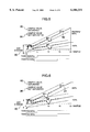
- FIG. 5 shows input waveforms of the ADC 213 and sample values of side samples when thermal asperity occurs in a least-dense pattern ("0" having a run length of 7).
- FIG. 6 shows input waveforms of the ADC 213 and sample values of peak samples when thermal asperity occurs in a least-dense pattern.
- This graph shows two types of TA waveforms depending on a size (Ata/Asig) thereof, i.e., a waveform 83 with a size of 300% and a waveform 84 with a size of 100%.
- a waveform 83 with a size of 300% When the ADC dynamic range 80 is ⁇ 1 V and the peak value 81 of the input waveform is ⁇ 0.8 V, the side sample values 82 are about ⁇ 0.6 V.
- a sample value 85 indicated by a circle is saturated and a sample value 86 indicated by a solid circle is not saturated.
- the detect ion of thermal asperity is delayed, the change-over of the cut off frequency is delayed for the HPF 210 and hence the amplitude of thermal asperity be comes greater.
- the saturation period is elongated in the ADC 213 and the period in which the AGC and PLL loops are not controlled becomes longer, this leads to an unstable operation.
- the saturation period is elongated in the ADC 213 and the period in which the AGC and PLL loops are not controlled becomes longer, this leads to an unstable operation.
- the low-frequency component is removed from the signal and hence the reproduction performance is deteriorated.
- thermal asperity is assumed and a result of TA detection (TADETD) is produced.
- TADETD TA detection
- the period of eight samples is checked to detect occurrence of thermal asperity in random data, not only in the least-dense pattern. Thanks to the provision, thermal asperity with a large amplitude (e.g., 300%) can be detected with a high precision at a high speed.
- FIG. 14 shows a block diagram of an internal configuration of the TADET2 242.
- the output data from the ADC 213 is respectively compared with a positive saturation value and a negative saturation value, and there is produced "1" when a matching condition results.
- the positive and negative saturation values are, for example, "011111” and "100000" when the output from the ADC 213 includes six bits in expression of 2's complement.
- Shift registers 347 and 348 store therein seven samples of outputs respectively from the comparators 345 and 346.
- Adders 349 and 350 respectively add the seven samples respectively outputted from the shift registers 347 and 348 to outputs (each including one sample) respectively from the comparators 345 and 346, namely, a total of eight (M) sample are handled for the addition of comparison results.
- the DVCOC 222 sets the control output to "0" (i.e., the control output is invalidated) in response to TASW3 outputted from the TASHRT 243 at detection of thermal asperity.
- the abnormal signal is detected in the DVCOC 222 in accordance with the pattern of input data (outputted from the DEQ 214) to thereby automatically set the control output to "0".
- input data is expressed as X and an expected value (+1, 0, -1) attained by conducting the hard detection for the input data is denoted as Y
- the phase error Z can be derived from the following expression.
- the reproducing circuit (RSPC 201A) of the magnetic disk unit 10A in which the magnetoresistive head 3 is used as its reproducing head even when the amplitude is decreased in the data signal region due to thermal asperity and/or a medium defect, it is possible to suppress disturbance in the quantities of control of the AGC and PLL loops, which consequently prevents the burst error in data due to the disturbed operation of the AGC and PLL loops.
- the VGA 211 does not minimize the gain. Therefore, it is possible to prevent the sector error which is caused because the sync byte cannot be detected due to an insufficient control operation of the AGC and PLL loops.
- a high-performance reproducing circuit (RSPC 201A) and a high-performance magnetic disk unit 10A in which even when the amplitude is decreased due to thermal asperity and/or a medium defect of a magnetic disk 2, the signal can be reproduced on the fly without conducting any retry or the like.
- the reproduced signal processing technology of the present invention is applied to a reproduce signal processing system of a magnetic disk unit.
- the reproduced signal processing technology of the present invention can be applied to a pre-stage of a maximum likelihood decoding system in an information communication facility employing the maximum likelihood decoding in the processing of signals received from a desired communication medium.
- the magnetic storage unit of the present invention there can be obtained an advantageous effect by a relatively small-sized circuit that the influence of thermal asperity and/or an amplitude reduction can be removed from a reproduced signal onto which a noise due to thermal asperity or the like is superimposed and/or a reproduced signal of which an amplitude is lowered due to a medium defect.
Abstract
Description
                                  TABLE 1
__________________________________________________________________________
Setting and conditions of HPF cutoff frequency of the
present invention
SW1 SW2 fc (MHz)
              Condition
__________________________________________________________________________
off off 1     SRV = "L"&(TADET0 + TADET1 + TADET2) = "L"
off on  6     RG = "H"&(TADET0 + TADET1 + TADET2) = "H"
on  off 9     don't use
on  on  15    SRV = "H"
__________________________________________________________________________
 &* Logical product operation
 +* Logical sum operation
Z.sub.K ÷Z.sub.K-1 =-(X.sub.K -X.sub.K-2)*Y.sub.K-1 +(Y.sub.K -Y.sub.K-2)*X.sub.K-1 (1)
              TABLE 2
______________________________________
Examples of operation by the digital VCO control circuit
in accordance with the present invention
Y.sub.k-2
      Y.sub.k-1
              Y.sub.k
                     Expression for operation
                                   Remarks
______________________________________
-1    -1      -1     0             Abnormal signal
-1    -1       0     (X.sub.k- X.sub.k-2) + X.sub.k-1
-1    -1      +1     (X.sub.k- X.sub.k-2) + 2X.sub.k-1
-1     0      -1     0             Abnormal signal
-1     0       0     X.sub.k-1
-1     0      +1     2X.sub.k-1
-1    +1      -1     0             Abnormal signal
-1    +1       0
(X.sub.k- X.sub.k-2) + X.sub.k-1
-1    +1      +1
(X.sub.k- X.sub.k-2) + 2X.sub.k-1
 0    -1      -1     (X.sub.k- X.sub.k-2) - X.sub.k-1
 0    -1       0     (X.sub.k- X.sub.k-2)
 0    -1      +1     (X.sub.k- X.sub.k-2) + X.sub.k-1
 0     0      -1
X.sub.k-1
 0     0       0     0
 0     0      +1     X.sub.k-1
 0    +1      -1
(X.sub.k- X.sub.k-2) - X.sub.k-1
 0    +1       0
(X.sub.k- X.sub.k-2)
 0    +1      +1
(X.sub.k- X.sub.k-2) + X.sub.k-1
+1    -1      -1     (X.sub.k- X.sub.k-2) - 2X.sub.k-1
+1    -1       0     (X.sub.k- X.sub.k-2) - X.sub.k-1
+1    -1      +1     0             Abnormal signal
+1     0      -1
2X.sub.k-1
+1     0       0
X.sub.k-1
+1     0      +1     0             Abnormal signal
+1    +1      -1
(X.sub.k- X.sub.k-2) - 2X.sub.k-1
+1    +1       0
(X.sub.k- X.sub.k-2) - X.sub.k-1
+1    +1      +1     0             Abnormal signal
______________________________________
Claims (27)
Applications Claiming Priority (2)
| Application Number | Priority Date | Filing Date | Title |
|---|---|---|---|
| JP26525297A JP3545579B2 (en) | 1997-09-30 | 1997-09-30 | Reproduction signal processing method, reproduction signal processing circuit, and magnetic storage device |
| JP9-265252 | 1997-09-30 |
Publications (1)
| Publication Number | Publication Date |
|---|---|
| US6104331A true US6104331A (en) | 2000-08-15 |
Family
ID=17414656
Family Applications (1)
| Application Number | Title | Priority Date | Filing Date |
|---|---|---|---|
| US09/161,734 Expired - Lifetime US6104331A (en) | 1997-09-30 | 1998-09-29 | Reproduced signal processing method, reproduced signal processing circuit, and a magnetic storage apparatus |
Country Status (2)
| Country | Link |
|---|---|
| US (1) | US6104331A (en) |
| JP (1) | JP3545579B2 (en) |
Cited By (9)
| Publication number | Priority date | Publication date | Assignee | Title |
|---|---|---|---|---|
| WO2002097809A1 (en) * | 2001-05-22 | 2002-12-05 | Seagate Technology Llc | Low amplitude skip write detector |
| US20040012513A1 (en) * | 2000-07-17 | 2004-01-22 | Laure Van Schendel | Analog-to-digital conversion method and device |
| US20040021970A1 (en) * | 2001-04-13 | 2004-02-05 | Nobuhiro Kondo | Magnetically erecorded data reproduction apparatus and method |
| US20040027264A1 (en) * | 2000-06-06 | 2004-02-12 | Stefan Otte | Method for providing a digital current fluctuation signal |
| US20040102164A1 (en) * | 2002-09-23 | 2004-05-27 | Karim-Thomas Taghizadeh-Kaschani | Receiver circuit for a push-pull transmission method and method for receiver-end signal processing in push-pull transmission methods |
| US20050219725A1 (en) * | 2004-03-31 | 2005-10-06 | Kemal Ozanoglu | Read head preamplifier with thermal asperity transient control |
| US20070182860A1 (en) * | 2006-02-08 | 2007-08-09 | Jin-Ho Kwon | Gain control circuit and method of controlling gain |
| EP2369585A1 (en) * | 2010-03-23 | 2011-09-28 | LSI Corporation | Amplitude-based approach for detection and classification of hard-disc defect regions |
| US20110235204A1 (en) * | 2010-03-25 | 2011-09-29 | Lsi Corporation | Detection of hard-disc defect regions using soft decisions |
Families Citing this family (1)
| Publication number | Priority date | Publication date | Assignee | Title |
|---|---|---|---|---|
| JP2001084506A (en) * | 1999-09-17 | 2001-03-30 | Fujitsu Ltd | Noise elimination circuit, amplifier circuit, and magnetic recorder |
Citations (7)
| Publication number | Priority date | Publication date | Assignee | Title |
|---|---|---|---|---|
| US4914398A (en) * | 1988-08-01 | 1990-04-03 | International Business Machines Corporation | Method and circuitry to suppress additive disturbances in data channels containing MR sensors |
| US5057785A (en) * | 1990-01-23 | 1991-10-15 | International Business Machines Corporation | Method and circuitry to suppress additive disturbances in data channels |
| US5089757A (en) * | 1991-03-15 | 1992-02-18 | Maxtor Corporation | Synchronous digital detection of position error signal |
| US5233482A (en) * | 1991-07-31 | 1993-08-03 | International Business Machines Corporation | Thermal asperity compensation for PRML data detection |
| JPH0786964A (en) * | 1993-07-23 | 1995-03-31 | Victor Co Of Japan Ltd | Error correcting device |
| US5559772A (en) * | 1993-02-17 | 1996-09-24 | Canon Kabushiki Kaisha | Information recording and/or reproducing apparatus and method for adjusting an offset amount of a focusing servo circuit |
| US5847890A (en) * | 1996-07-31 | 1998-12-08 | Kabushiki Kaisha Toshiba | Magnetic disk apparatus and a thermal asperity compensation method of the same |
-
1997
- 1997-09-30 JP JP26525297A patent/JP3545579B2/en not_active Expired - Fee Related
-
1998
- 1998-09-29 US US09/161,734 patent/US6104331A/en not_active Expired - Lifetime
Patent Citations (8)
| Publication number | Priority date | Publication date | Assignee | Title |
|---|---|---|---|---|
| US4914398A (en) * | 1988-08-01 | 1990-04-03 | International Business Machines Corporation | Method and circuitry to suppress additive disturbances in data channels containing MR sensors |
| US5057785A (en) * | 1990-01-23 | 1991-10-15 | International Business Machines Corporation | Method and circuitry to suppress additive disturbances in data channels |
| US5089757A (en) * | 1991-03-15 | 1992-02-18 | Maxtor Corporation | Synchronous digital detection of position error signal |
| US5233482A (en) * | 1991-07-31 | 1993-08-03 | International Business Machines Corporation | Thermal asperity compensation for PRML data detection |
| JPH0628785A (en) * | 1991-07-31 | 1994-02-04 | Internatl Business Mach Corp <Ibm> | Method and apparatus for compensation of thermal asperity regarding date detection in data channel and direct access storage device |
| US5559772A (en) * | 1993-02-17 | 1996-09-24 | Canon Kabushiki Kaisha | Information recording and/or reproducing apparatus and method for adjusting an offset amount of a focusing servo circuit |
| JPH0786964A (en) * | 1993-07-23 | 1995-03-31 | Victor Co Of Japan Ltd | Error correcting device |
| US5847890A (en) * | 1996-07-31 | 1998-12-08 | Kabushiki Kaisha Toshiba | Magnetic disk apparatus and a thermal asperity compensation method of the same |
Cited By (22)
| Publication number | Priority date | Publication date | Assignee | Title |
|---|---|---|---|---|
| US20040027264A1 (en) * | 2000-06-06 | 2004-02-12 | Stefan Otte | Method for providing a digital current fluctuation signal |
| US6861966B2 (en) * | 2000-06-06 | 2005-03-01 | Leopold Kostal Gmbh & Co. Kg | Method for providing a digital current fluctuation signal |
| US20040012513A1 (en) * | 2000-07-17 | 2004-01-22 | Laure Van Schendel | Analog-to-digital conversion method and device |
| US6940442B2 (en) * | 2000-07-17 | 2005-09-06 | Nortel Networks France | Analog-to-digital conversion of a radiocommunication signal |
| US7088536B2 (en) | 2001-04-13 | 2006-08-08 | Sony Corporation | Magnetically recorded data reproduction apparatus and method thereof |
| US20040021970A1 (en) * | 2001-04-13 | 2004-02-05 | Nobuhiro Kondo | Magnetically erecorded data reproduction apparatus and method |
| GB2385978A (en) * | 2001-05-22 | 2003-09-03 | Seagate Technology Llc | Low amplitude skip write detector |
| WO2002097809A1 (en) * | 2001-05-22 | 2002-12-05 | Seagate Technology Llc | Low amplitude skip write detector |
| GB2385978B (en) * | 2001-05-22 | 2004-11-24 | Seagate Technology Llc | Low amplitude skip write detector |
| US7457373B2 (en) * | 2002-09-23 | 2008-11-25 | Infineon Technologies Ag | Receiver circuit for a push-pull transmission method and method for receiver-end signal processing in push-pull transmission methods |
| US20040102164A1 (en) * | 2002-09-23 | 2004-05-27 | Karim-Thomas Taghizadeh-Kaschani | Receiver circuit for a push-pull transmission method and method for receiver-end signal processing in push-pull transmission methods |
| EP1585130A2 (en) * | 2004-03-31 | 2005-10-12 | STMicroelectronics, Inc. | Read head preamplifier with thermal asperity transient control |
| EP1585130A3 (en) * | 2004-03-31 | 2005-12-14 | STMicroelectronics, Inc. | Read head preamplifier with thermal asperity transient control |
| US20050219725A1 (en) * | 2004-03-31 | 2005-10-06 | Kemal Ozanoglu | Read head preamplifier with thermal asperity transient control |
| US7274523B2 (en) | 2004-03-31 | 2007-09-25 | Stmicroelectronics, Inc. | Read head preamplifier with thermal asperity transient control |
| US20070182860A1 (en) * | 2006-02-08 | 2007-08-09 | Jin-Ho Kwon | Gain control circuit and method of controlling gain |
| US8045059B2 (en) * | 2006-02-08 | 2011-10-25 | Samsung Electronics Co., Ltd. | Gain control circuit and method of controlling gain |
| EP2369585A1 (en) * | 2010-03-23 | 2011-09-28 | LSI Corporation | Amplitude-based approach for detection and classification of hard-disc defect regions |
| CN102201264A (en) * | 2010-03-23 | 2011-09-28 | Lsi公司 | Amplitude-based approach for detection and classification of hard-disc defect regions |
| CN102201264B (en) * | 2010-03-23 | 2014-05-14 | Lsi公司 | Amplitude-based approach for detection and classification of hard-disc defect regions |
| US20110235204A1 (en) * | 2010-03-25 | 2011-09-29 | Lsi Corporation | Detection of hard-disc defect regions using soft decisions |
| US8089713B2 (en) | 2010-03-25 | 2012-01-03 | Lsi Corporation | Detection of hard-disc defect regions using soft decisions |
Also Published As
| Publication number | Publication date |
|---|---|
| JPH11102503A (en) | 1999-04-13 |
| JP3545579B2 (en) | 2004-07-21 |
Similar Documents
| Publication | Publication Date | Title |
|---|---|---|
| KR100299083B1 (en) | Magnetic disk device and retry method using it | |
| US7334165B2 (en) | Signal processing apparatus and a data recording and reproducing apparatus including local memory processor | |
| US6490691B1 (en) | Error recovery in a disk drive | |
| US5844509A (en) | Synchronous read channel employing a data randomizer | |
| KR100555277B1 (en) | Servo demodulator and method for synchronous servo demodulation | |
| US6081397A (en) | Method and apparatus for SID-to-SID period estimation | |
| JP3162253B2 (en) | Decoding method of head positioning servo information and synchronous servo data detection subsystem | |
| US6657803B1 (en) | Method and apparatus for data error recovery using defect threshold detector and viterbi gain | |
| KR100305551B1 (en) | Magnetic disk device and its error data correction device and error data correction method | |
| US6052804A (en) | Data transfer optimization through sector evaluation and reallocation during a disc drive idle mode | |
| US6178053B1 (en) | Storage apparatus for reducing a read error caused by a thermal asperity of a magneto-resistive head | |
| US6101227A (en) | Detector and method for detecting defects in the magnetic media of a mass storage system | |
| US6493165B1 (en) | Magnetic disk drive | |
| IE921713A1 (en) | Fault Tolerant RLL Data Sector Address Mark Decoder | |
| JP2004014090A (en) | Data reproduction system, reproduction method and circuit for performing controlling of reproduction system | |
| US5847890A (en) | Magnetic disk apparatus and a thermal asperity compensation method of the same | |
| US6104331A (en) | Reproduced signal processing method, reproduced signal processing circuit, and a magnetic storage apparatus | |
| US6760173B2 (en) | Synchronization servo mark detector and method having improved phase error immunity for use in mass data storage device, or the like | |
| US6101229A (en) | Data synchronization method and circuit using a timeout counter | |
| US7952825B2 (en) | Method and apparatus adjusting reference clock frequency and disk drive using same | |
| US7817365B2 (en) | Address mark detection with error threshold that varies with timing jitter | |
| US6055118A (en) | Holding automatic gain control levels during read error recovery in a disc drive | |
| US20020023248A1 (en) | Medium defect detection method and data storage apparatus | |
| US6707626B2 (en) | Apparatus and method for detecting SYNC signals written on a disk memory device | |
| US7924522B2 (en) | Apparatus and method of detecting error symbol, and disk drive apparatus using the same |
Legal Events
| Date | Code | Title | Description |
|---|---|---|---|
| AS | Assignment |
Owner name: HITACHI LTD., JAPAN Free format text: ASSIGNMENT OF ASSIGNORS INTEREST;ASSIGNORS:ISHIDA, YOSHITERU;SATOH, NAOKI;TAKASHI, TERUMI;AND OTHERS;REEL/FRAME:009509/0699 Effective date: 19980914 |
|
| STCF | Information on status: patent grant |
Free format text: PATENTED CASE |
|
| AS | Assignment |
Owner name: HITACHI GLOBAL STORAGE TECHNOLOGIES JAPAN, LTD., J Free format text: ASSIGNMENT OF ASSIGNORS INTEREST;ASSIGNOR:HITACHI, LTD.;REEL/FRAME:014788/0751 Effective date: 20031120 |
|
| FPAY | Fee payment |
Year of fee payment: 4 |
|
| FEPP | Fee payment procedure |
Free format text: PAYOR NUMBER ASSIGNED (ORIGINAL EVENT CODE: ASPN); ENTITY STATUS OF PATENT OWNER: LARGE ENTITY |
|
| FPAY | Fee payment |
Year of fee payment: 8 |
|
| FEPP | Fee payment procedure |
Free format text: PAYER NUMBER DE-ASSIGNED (ORIGINAL EVENT CODE: RMPN); ENTITY STATUS OF PATENT OWNER: LARGE ENTITY Free format text: PAYOR NUMBER ASSIGNED (ORIGINAL EVENT CODE: ASPN); ENTITY STATUS OF PATENT OWNER: LARGE ENTITY |
|
| FPAY | Fee payment |
Year of fee payment: 12 |
|
| AS | Assignment |
Owner name: WESTERN DIGITAL TECHNOLOGIES, INC., CALIFORNIA Free format text: ASSIGNMENT OF ASSIGNORS INTEREST;ASSIGNOR:HGST NETHERLANDS B.V.;REEL/FRAME:040818/0551 Effective date: 20160831 |