BACKGROUND OF THE INVENTION
1. Field of Invention
The present invention relates to a flash EPROM structure. More particularly, the present invention relates to a method for forming ETOX cells (Intel Type Flash EPROM Cells) using a self-aligned source etching process.
2. Description of Related Art
Erasable programmable ROM (EPROM) is a type of memory circuit commonly used in computer and electronic products. The advantage of EPROM is that stored data or programs will not be erased under normal circumstances. However, if the data or program really need to be erased, this can be done by shining an ultraviolet (UV) light source onto the EPROM for a period. Once the data or programs have been removed, new data or programs can then be entered and stored. Because all the old data and programs are lost during the EPROM erasing process and everything needs to be re-entered from scratch, much time is wasted in the process. In view of this, Intel Corp. has developed and introduced a kind of memory known as flash EPROM to the market. Data in the flash EPROM will not be completely wiped out in a single erase operation. Instead, data can be locally amended block by block. When the dimensions of flash EPROM are miniaturized, a self-aligned source etching process becomes the obvious choice for forming the ETOX cells. However, in a conventional method of producing ETOX cells, the plasma-etching operation will damage the oxide/nitride/oxide (ONO) layer. This will result in charge retention and reliability problems.
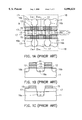
FIG. 1A is a layout diagram for a collection of ETOX cells formed by the conventional self-aligned source etching process. As shown in FIG. 1A, the labeled items include floating gates 13, control gates 15, masks 18, field oxide layers 17, drain regions 16b and a common source region 16a, which is patterned out according to masks 18. The area labeled 9 within a dotted rectangle is the location of an ETOX cell.
FIG. 1B is a cross-section along line I-I' in FIG. 1A. As shown in FIG. 1B, the ETOX cell comprises a gate, a common source region 16a and a drain region 16b. The gate is a four-layered stack including a tunnel oxide layer 12, a floating gate 13, an ONO layer 14 and a controlling gate 15. The controlling gate 15 and the floating gate 13 together constitute a gate terminal. The common source region 16a and the drain region 16b are formed in a substrate 11 on each side of the gate.
FIG. 1C is a cross-section along line II-II' in FIG. 1A. As shown in FIG. 1C, a field oxide layer is formed above the substrate 11, and that the controlling gate 15 is formed above the field oxide layer 17.
FIGS. 2A and 2B are cross-sectional views showing the progression of manufacturing steps in the production of ETOX cell by a conventional self-aligned source etching process. The cross-sectional line along which FIGS. 2A and 2B are derived from is the same as in FIG. 1C. First, a substrate structure having gates 15 and field oxide layers 17 already formed thereon is provided. The substrate structure here is similar to the one shown in FIG. 1C. The only difference between them is that a common source region 16a has not been formed in the substrate structure in FIG. 2A. Then, a photomask 18 is formed to cover the substrate and patterned such that locations of the common source regions 16a are exposed to get ready for subsequent processing operations.
Next, with reference to FIG. 1A, FIG. 1C and FIG. 2B, the exposed field oxide layer 17 is etched using a dry etching method having a high selectivity ratio. Thereafter, the photomask 18 is removed. This is followed by ion doping operations to form the common source region 16a and the drain region 16b. Because subsequent processes are familiar to those skilled in the art, detailed description is omitted here.
Because the conventional self-aligned source etching technique in forming the ETOX cells can easily damage the oxide/nitride/oxide layer of the gate, charge retention and reliability problems are quite common.
In light of the foregoing, there is a need in the art to improve the method of forming ETOX cells.
SUMMARY OF THE INVENTION
Accordingly, the present invention is directed to provide a method for forming ETOX cells using a self-aligned source etching process that can alleviate the charge retention and reliability problems due to in-process plasma damage of the ONO layer.
To achieve these and other advantages and in accordance with the purpose of the invention, as embodied and broadly described herein, the invention provides a method for forming ETOX cells by a self-aligned source etching process comprising the steps of first depositing a layer of dielectric, preferably a silicon nitride (Si3 N4) layer, to a thickness of 100 Å to 700 Å, then etching back the layer to form a silicon nitride spacer. Thereafter, the common source region is defined using a patterned photomask. Subsequently, the field oxide layer is etched using a wet etching method or a dry etching method having a high selectivity ratio.
The characteristic of this invention is the ability to protect the oxide/nitride/oxide layer against any damages by plasma during the self-aligned source etching process that may lead to charge retention and reliability problems.
It is to be understood that both the foregoing general description and the following detailed description are exemplary, and are intended to provide further explanation of the invention as claimed.
BRIEF DESCRIPTION OF THE DRAWINGS
The accompanying drawings are included to provide a further understanding of the invention and are incorporated in and constitute a part of this specification. The drawings illustrate embodiments of the invention and, together with the description, serve to explain the principles of the invention. In the drawings,
FIG. 1A is a layout diagram for a collection of ETOX cells formed by a conventional self-aligned source etching process;
FIG. 1B is a cross-section along line I-I' in FIG. 1A;
FIG. 1C is a cross-section along line II-II' in FIG. 1A;
FIGS. 2A and 2B are cross-sectional views showing the progression of manufacturing steps in the production of an ETOX cell using a conventional self-aligned source etching process;
FIG. 3A is a layout diagram for a collection of ETOX cells formed by a self-aligned source etching process according to one preferred embodiment of this invention;
FIG. 3B is a cross-section along line III-III' in FIG. 3A;
FIG. 3C is a cross-section along line IV-IV' in FIG. 3A;
FIGS. 4A through 4C are cross-sectional views along line III-III' of FIG. 3A showing the progression of manufacturing steps in the production of ETOX cell using a self-aligned source etching process according to one preferred embodiment of this invention; and
FIGS. 5A through 5C are cross-sectional views along line IV-IV' of FIG. 3A showing the progression of manufacturing steps in the production of ETOX cell using a self-aligned source etching process according to one preferred embodiment of this invention.
DESCRIPTION OF THE PREFERRED EMBODIMENTS
Reference will now be made in detail to the present preferred embodiments of the invention, examples of which are illustrated in the accompanying drawings. Wherever possible, the same reference numbers are used in the drawings and the description to refer to the same or like parts.
FIG. 3A is a layout diagram for a collection of ETOX cells formed by a self-aligned source etching process according to one preferred embodiment of this invention. As shown in FIG. 3A, the labeled items include floating gates 23, control gates 25, spacers 28, masks 29, field oxide layers 27, drain regions 26b and common source region 26a, which is patterned out according to masks 29. The area labeled 30 within a dotted rectangle is the location of an ETOX cell.
FIG. 3B is a cross-section along line III-III' in FIG. 3A. As shown in FIG. 3B, the ETOX cell comprises a gate, a common source region 26a and a drain region 26b. The gate is a four-layered stack including a tunnel oxide layer 22, a floating gate 23, an ONO layer 24 and a controlling gate 25. The controlling gate 25 and the floating gate 23 together constitute a gate terminal. The common source region 26a and the drain region 26b are formed in a substrate 21 on each side of the gate.
FIG. 3C is a cross-section along line IV-IV' in FIG. 3A. As shown in FIG. 3C, a field oxide layer is formed above the substrate 21, and that the controlling gate 25 is formed above the field oxide layer 27.
FIGS. 4A through 4C are cross-sectional views along line III-III' of FIG. 3A showing the progression of manufacturing steps in the production of ETOX cell using a self-aligned source etching process according to one preferred embodiment of this invention. As shown in FIG. 4A, a substrate structure that has gates 25 and field oxide layers 27 already formed thereon is provided. The substrate structure here is similar to the one shown in FIG. 3B. The cross-sectional line along which FIGS. 4A through 4C are derived from is the same as in FIG. 3B. The only difference between them is that a common source region 26a, drain regions 26b, and spacers 28 has not yet been formed in the substrate structure in FIG. 4A. The spacers 28 are formed by depositing a dielectric layer, preferably a silicon nitride (Si3 N4) layer, to a thickness of 100 to 700, over the substrate structure, then etching back the dielectric layer to form a silicon nitride spacer 28 on the two sidewalls of a gate stack. Therefore, the ONO layer 24 is being protected by the spacer layer 28 as shown in FIG. 4B.
FIGS. 5A through 5C are cross-sectional views along line IV-IV' of FIG. 3A showing the progression of manufacturing steps in the production of ETOX cell using a self-aligned source etching process according to one preferred embodiment of this invention. The substrate structure is the same as in FIGS. 4A through 4C. Moreover, the cross-sectional line along which FIGS. 5A through 5C are derived from is the same as in FIG. 3C.
Next, with reference to FIG. 4B and FIG. 5B, a photomask 29 is used to form a pattern of the desired common source regions in the substrate 21.
Next, with reference to FIG. 3C and FIG. 5C, either a dry etching method having a high selectivity ratio such as a plasma etching method, or a wet etching method using a buffered oxide etchant (BOE) is used to etch away the exposed field oxide layer 27. The field oxide layer 27 is etched until the substrate surface 21 is reached, thereby exposing the desired common source locations. Thereafter, the photomask 29 is removed, and then ions are doped to form the common source region 26a and the drain regions 26b. Finally, subsequent conventional processes are performed.
Since the sequence of steps in the production of ETOX cells by the self-aligned source etching process in this invention involves forming spacers 28 first, then etching the field oxide layer 27, and finally performing an ion doping operation, damages to the ONO layer 24 during the plasma etching step is minimal. Hence, charge retention and reliability problems can be avoided.
It will be apparent to those skilled in the art that various modifications and variations can be made to the structure of the present invention without departing from the scope or spirit of the invention. In view of the foregoing, it is intended that the present invention cover modifications and variations of this invention provided they fall within the scope of the following claims and their equivalents.