US6090464A - Reinforced substrate and flat panel display employing the same - Google Patents
Reinforced substrate and flat panel display employing the same Download PDFInfo
- Publication number
- US6090464A US6090464A US09/070,740 US7074098A US6090464A US 6090464 A US6090464 A US 6090464A US 7074098 A US7074098 A US 7074098A US 6090464 A US6090464 A US 6090464A
- Authority
- US
- United States
- Prior art keywords
- reinforcing structure
- flat panel
- panel display
- array
- substrate
- Prior art date
- Legal status (The legal status is an assumption and is not a legal conclusion. Google has not performed a legal analysis and makes no representation as to the accuracy of the status listed.)
- Expired - Lifetime
Links
- 239000000758 substrate Substances 0.000 title claims abstract description 91
- 230000003014 reinforcing effect Effects 0.000 claims abstract description 65
- 239000011521 glass Substances 0.000 claims abstract description 11
- 230000001681 protective effect Effects 0.000 claims description 12
- 239000004020 conductor Substances 0.000 claims description 6
- 239000007888 film coating Substances 0.000 claims 4
- 238000009501 film coating Methods 0.000 claims 4
- 238000005452 bending Methods 0.000 abstract description 5
- 239000000463 material Substances 0.000 abstract description 4
- 239000002184 metal Substances 0.000 abstract description 2
- 239000012780 transparent material Substances 0.000 description 5
- 239000000356 contaminant Substances 0.000 description 4
- 239000000428 dust Substances 0.000 description 4
- 238000004519 manufacturing process Methods 0.000 description 3
- 238000005401 electroluminescence Methods 0.000 description 2
- 239000004973 liquid crystal related substance Substances 0.000 description 2
- 239000012811 non-conductive material Substances 0.000 description 2
- 239000012769 display material Substances 0.000 description 1
- 230000000007 visual effect Effects 0.000 description 1
Images


Classifications
-
- G—PHYSICS
- G09—EDUCATION; CRYPTOGRAPHY; DISPLAY; ADVERTISING; SEALS
- G09F—DISPLAYING; ADVERTISING; SIGNS; LABELS OR NAME-PLATES; SEALS
- G09F9/00—Indicating arrangements for variable information in which the information is built-up on a support by selection or combination of individual elements
- G09F9/30—Indicating arrangements for variable information in which the information is built-up on a support by selection or combination of individual elements in which the desired character or characters are formed by combining individual elements
-
- Y—GENERAL TAGGING OF NEW TECHNOLOGICAL DEVELOPMENTS; GENERAL TAGGING OF CROSS-SECTIONAL TECHNOLOGIES SPANNING OVER SEVERAL SECTIONS OF THE IPC; TECHNICAL SUBJECTS COVERED BY FORMER USPC CROSS-REFERENCE ART COLLECTIONS [XRACs] AND DIGESTS
- Y10—TECHNICAL SUBJECTS COVERED BY FORMER USPC
- Y10T—TECHNICAL SUBJECTS COVERED BY FORMER US CLASSIFICATION
- Y10T428/00—Stock material or miscellaneous articles
- Y10T428/23—Sheet including cover or casing
- Y10T428/234—Sheet including cover or casing including elements cooperating to form cells
- Y10T428/236—Honeycomb type cells extend perpendicularly to nonthickness layer
-
- Y—GENERAL TAGGING OF NEW TECHNOLOGICAL DEVELOPMENTS; GENERAL TAGGING OF CROSS-SECTIONAL TECHNOLOGIES SPANNING OVER SEVERAL SECTIONS OF THE IPC; TECHNICAL SUBJECTS COVERED BY FORMER USPC CROSS-REFERENCE ART COLLECTIONS [XRACs] AND DIGESTS
- Y10—TECHNICAL SUBJECTS COVERED BY FORMER USPC
- Y10T—TECHNICAL SUBJECTS COVERED BY FORMER US CLASSIFICATION
- Y10T428/00—Stock material or miscellaneous articles
- Y10T428/24—Structurally defined web or sheet [e.g., overall dimension, etc.]
- Y10T428/24149—Honeycomb-like
- Y10T428/24165—Hexagonally shaped cavities
-
- Y—GENERAL TAGGING OF NEW TECHNOLOGICAL DEVELOPMENTS; GENERAL TAGGING OF CROSS-SECTIONAL TECHNOLOGIES SPANNING OVER SEVERAL SECTIONS OF THE IPC; TECHNICAL SUBJECTS COVERED BY FORMER USPC CROSS-REFERENCE ART COLLECTIONS [XRACs] AND DIGESTS
- Y10—TECHNICAL SUBJECTS COVERED BY FORMER USPC
- Y10T—TECHNICAL SUBJECTS COVERED BY FORMER US CLASSIFICATION
- Y10T428/00—Stock material or miscellaneous articles
- Y10T428/24—Structurally defined web or sheet [e.g., overall dimension, etc.]
- Y10T428/24174—Structurally defined web or sheet [e.g., overall dimension, etc.] including sheet or component perpendicular to plane of web or sheet
Definitions
- the present invention relates to a reinforced substrate for a flat panel display and a flat panel display using the same, and more particularly, to a reinforced substrate and an improved flat panel display which can prevent deformation of a substrate without increasing the thickness of the substrate when a flat panel display is large.
- a flat panel display for displaying pictures can be a liquid crystal display, a plasma display panel, an electroluminescence element, etc.
- a flat panel display consumes significantly less power than other devices, can be produced in various sizes ranging from subminiature to a large size, and can have diverse display patterns. Therefore, flat panel displays occupy an important position in the field of display devices.
- a conventional flat panel display has upper and lower substrates at least one of which is made of a transparent material such as glass or plastic to allow light to penetrate, and has the shape of a flat plate in order to have uniform refractive properties.
- Such a conventional flat panel display must have an enlarged substrate to provide a large display area (e.g., 40 inches or more in one direction). As the area of the substrate increases, its thickness must be also increased in order to maintain the flatness of the substrate. A thick substrate impedes manufacture of a flat panel display because of its weight, reduces transmissivity of display light, and increases manufacturing costs.
- a reinforced substrate for a flat panel display having a reinforcing structure formed on one surface of the substrate, for preventing bending of the substrate.
- a reinforced substrate for a flat panel display comprising a substrate and a reinforcing structure formed on one surface of the substrate for preventing bending of the substrate.
- a flat panel display comprising two substrates, a display generating material interposed between the two substrates under a sealed condition, and a reinforcing structure on one surface of at least one of the substrates for preventing bending of the substrate.
- the reinforcing structure comprises an array of hollow polygonal pillars or cylinders.
- the array is made of transparent glass or plastic.
- the array is made of an electrically conductive material.
- the array is preferably grounded.
- the reinforcing structure may further include an electrically conductive film which is coated on one end surface of the array.
- the side of the reinforcing structure which does not contact the substrate may have a transparent protective member formed thereon.
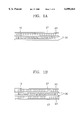
- FIGS. 1A and 1B are cross-sectional views of a flat panel display to which a reinforced substrate according to the present invention is applied, the flat panel display of FIG. 1A having a single reinforced substrate and the flat panel display of FIG. 1B having two reinforced substrates;
- FIG. 2 is a perspective view illustrating a reinforced substrate for a flat panel display according to a first embodiment of the present invention
- FIG. 3 is a perspective view illustrating a reinforced substrate for a flat panel display according to a second embodiment of the present invention.
- FIG. 4 is a perspective view illustrating a reinforced substrate for a flat panel display according to a third embodiment of the present invention.
- FIGS. 1A and 1B are cross-sectional views showing a flat panel display employing a reinforcing structure associated with at least one of two substrates, according to the present invention.
- the flat panel display has a reinforcing structure 23 associated with at least one of two substrates 20 installed on both sides of a display generating portion 10 filled with a display material.
- the display generating portion 10 may be of any type appropriate for the type of visual display which the flat panel display is intended to generate. For example, it may be a liquid crystal display, a plasma display panel or an electroluminescence element.
- a reinforcing structure 23 is installed on the outer surface of one or both substrates 20.
- the flat panel display of FIG. 1A has a reinforcing structure 23 installed on only one of its two substrates 20, while the flat panel display of FIG. 1B has a reinforcing structure 23 installed on each of its two substrates 20.
- the reinforcing structure 23 is an array of hollow polygonal pillars or hollow cylinders made of transparent glass or plastic.
- An electrically conductive film can be coated on one end surface (upper surface) of the array of hollow polygonal pillars or hollow cylinders and be grounded.
- the reinforcing structure 23 is made of an electrically conductive material, the hollow polygonal pillars or hollow cylinders can be grounded.
- a protective member 27 is installed on the upper portion (one end surface) of the reinforcing structure 23. The protective member 27 prevents the inside of the reinforcing structure 23 from collecting contaminants such as dust and protects it from damage.
- the protective member 27 is preferably made of a light, tough and transparent material, such as plastic.
- FIG. 2 shows a reinforced substrate according to a first embodiment of the present invention.
- a reinforced substrate has a substrate and a reinforcing structure 23 attached to the substrate 20 for reinforcing the substrate 20.
- a reinforcing structure can be installed on one surface of one or both substrates in a flat panel display.
- the reinforcing structure 23 is made of a transparent, electrically nonconductive material, such as glass or plastic, and is formed of an array of hollow hexagonal pillars or hollow cylinders. It is preferable that the area of one hexagonal pillar or cylinder corresponds to the area occupied by at least 10 pixels of the flat panel display.
- the reinforcing structure 23 preferably has a protective member 27 made of a light, tough and transparent material, such as plastic, in order to prevent the inside of the reinforcing structure 23 from collecting contaminants such as dust and to protect it from damage.
- the protective member 27 is attached to the side of the reinforcing structure 23 which does not contact the substrate 20.
- FIG. 3 is a perspective view illustrating a reinforced substrate for a flat panel display according to a second embodiment of the present invention.
- a reinforced substrate has a substrate 20 and a reinforcing structure 23 attached to the substrate 20 for reinforcing the substrate 20, and an electrically conductive film 25 coated on one end surface (the upper surface) of the reinforcing structure 23.
- a reinforcing structure can be installed on one surface of one or both substrates in a flat panel display.
- the reinforcing structure 23 is made of a transparent, electrically nonconductive material, such as glass or plastic, and is formed of an array of hollow hexagonal pillars or hollow cylinders.
- the electrically conductive film 25 is coated on the end surface of the reinforcing structure 23 which does not contact the substrate 20, and the reinforcing structure 23 coated with the conductive film 25 is grounded via a ground unit 26, such that electromagnetic waves generated within the flat panel display are blocked.
- the reinforcing structure 23 preferably has a protective member 27 made of a light, tough and transparent material, such as plastic, in order to prevent the inside of the reinforcing structure 23 from collecting contaminants such as dust and to protect it from damage.
- the protective member 27 is attached on the conductive film 25.
- FIG. 4 is a perspective view illustrating a reinforced substrate for a flat panel display according to a third embodiment of the present invention.
- a reinforced substrate has a substrate 20 and a reinforcing structure 24 attached to the substrate 20, which is made of electrically conductive metal and formed of an array of hollow hexagonal pillars or hollow cylinders.
- the reinforcing structure 24 is grounded via a ground unit 26, such that electromagnetic waves generated within the flat panel display are blocked.
- the material of the reinforcing structure 24 preferably has a high electrical conductivity.
- Such a reinforcing structure can be installed on one surface of one or both substrates in a flat panel display.
- the reinforcing structure 24 preferably has a protective member 27 made of a light, tough and transparent material, in order to prevent the inside of the reinforcing structure 24 from collecting contaminants such as dust and to protect it from damage.
- the protective member 27 is attached to one end surface (the upper surface) of the reinforcing structure 24 which does not contact the substrate 20.
- a flat panel display when a flat panel display is manufactured in a large size, its flatness can be maintained simply by using one or two reinforced substrates according to the present invention which includes a reinforcing structure attached to one surface of the substrate, without increasing the thickness of the substrate. Since the large flat panel display uses a reinforced thin substrate rather than a thick substrate as in the prior art, more light is transmitted through the thin substrate. Also, the manufacturing cost of the substrate can be cut down, since the thickness of the substrate does not change. Furthermore, since a ground unit can be attached to the reinforcing structure, the flat panel display can block electromagnetic waves generated from its inside.
Landscapes
- Physics & Mathematics (AREA)
- General Physics & Mathematics (AREA)
- Engineering & Computer Science (AREA)
- Theoretical Computer Science (AREA)
- Devices For Indicating Variable Information By Combining Individual Elements (AREA)
- Liquid Crystal (AREA)
Abstract
Description
Claims (20)
Applications Claiming Priority (2)
| Application Number | Priority Date | Filing Date | Title |
|---|---|---|---|
| KR1019970067423A KR100277630B1 (en) | 1997-12-10 | 1997-12-10 | Flat display |
| KR97-67423 | 1997-12-10 |
Publications (1)
| Publication Number | Publication Date |
|---|---|
| US6090464A true US6090464A (en) | 2000-07-18 |
Family
ID=19526924
Family Applications (1)
| Application Number | Title | Priority Date | Filing Date |
|---|---|---|---|
| US09/070,740 Expired - Lifetime US6090464A (en) | 1997-12-10 | 1998-05-01 | Reinforced substrate and flat panel display employing the same |
Country Status (7)
| Country | Link |
|---|---|
| US (1) | US6090464A (en) |
| JP (2) | JPH11184399A (en) |
| KR (1) | KR100277630B1 (en) |
| CN (1) | CN1146942C (en) |
| FR (1) | FR2772176B1 (en) |
| NL (1) | NL1009037C2 (en) |
| TW (1) | TW479150B (en) |
Cited By (14)
| Publication number | Priority date | Publication date | Assignee | Title |
|---|---|---|---|---|
| US6429832B1 (en) * | 1998-09-11 | 2002-08-06 | Nec Corporation | Plasma display panel unit |
| US20040091672A1 (en) * | 2002-11-05 | 2004-05-13 | Jung-Keun Ahn | Plasma display panel |
| US20040169473A1 (en) * | 2003-01-22 | 2004-09-02 | Cha-Keun Yoon | Plasma display panel having delta pixel arrangement |
| US6837171B1 (en) | 2002-04-29 | 2005-01-04 | Palmer/Snyder Furniture Company | Lightweight table with unitized table top |
| US20050003148A1 (en) * | 2003-07-03 | 2005-01-06 | Myles Peter Robert William | Single panel glass structural panel and method of making same |
| USD533950S1 (en) * | 2004-02-26 | 2006-12-19 | Dan-Pal | Structural panel |
| US20070082138A1 (en) * | 2005-10-10 | 2007-04-12 | Electronics And Telecommunications Research Institute | Surface treatment method of fiber reinforced plastic substrate |
| US20080092788A1 (en) * | 2004-04-06 | 2008-04-24 | Luhao Leng | Kind of Desk |
| US20090117318A1 (en) * | 2004-04-06 | 2009-05-07 | Luhao Leng | Composite Desk |
| US20090256781A1 (en) * | 2008-04-14 | 2009-10-15 | Do-Hyuk Kwon | Film unit and plasma display panel having the same |
| US20110289869A1 (en) * | 2010-05-27 | 2011-12-01 | Paul August Jaster | Thermally insulating fenestration devices and methods |
| US9816675B2 (en) | 2015-03-18 | 2017-11-14 | Solatube International, Inc. | Daylight collectors with diffuse and direct light collection |
| US9816676B2 (en) | 2015-03-18 | 2017-11-14 | Solatube International, Inc. | Daylight collectors with diffuse and direct light collection |
| US20230304296A1 (en) * | 2022-03-22 | 2023-09-28 | Tanager Products, Inc. | Moisture porous building furring strip |
Families Citing this family (5)
| Publication number | Priority date | Publication date | Assignee | Title |
|---|---|---|---|---|
| JP4722082B2 (en) * | 2007-05-17 | 2011-07-13 | シャープ株式会社 | Backlight device and display device |
| JP2010191267A (en) * | 2009-02-19 | 2010-09-02 | Fuji Xerox Co Ltd | Image display medium and image display device |
| EP2610939B1 (en) | 2011-12-30 | 2018-02-07 | Samsung Electronics Co., Ltd. | Display device |
| EP2685444B1 (en) * | 2012-07-13 | 2017-03-08 | LG Electronics, Inc. | Display device using sandwich honeycomb panel |
| KR101966739B1 (en) * | 2012-11-09 | 2019-04-09 | 삼성전자주식회사 | Curved display apparatus |
Citations (7)
| Publication number | Priority date | Publication date | Assignee | Title |
|---|---|---|---|---|
| US3103460A (en) * | 1963-09-10 | Picket | ||
| US3137602A (en) * | 1959-08-21 | 1964-06-16 | Continental Can Co | Ceramic honeycomb |
| US4724010A (en) * | 1986-06-19 | 1988-02-09 | Teijin Limited | Solar cell module |
| US4803108A (en) * | 1987-05-01 | 1989-02-07 | Essex Specialty Products, Inc. | Honeycomb reinforcing sheet for the reinforcement of panels and method of reinforcing panels |
| US5524381A (en) * | 1991-03-19 | 1996-06-11 | Chahroudi; Day | Solar heated building designs for cloudy winters |
| US5796854A (en) * | 1997-03-04 | 1998-08-18 | Compaq Computer Corp. | Thin film speaker apparatus for use in a thin film video monitor device |
| US5831374A (en) * | 1996-01-12 | 1998-11-03 | Matsushita Electric Industrial Co., Ltd. | Plasma display panel, method of fabricating the same, and display apparatus using the plasma display panel |
Family Cites Families (5)
| Publication number | Priority date | Publication date | Assignee | Title |
|---|---|---|---|---|
| JPS5528004A (en) * | 1978-08-18 | 1980-02-28 | Canon Inc | Liquid crystal display element |
| GB8703306D0 (en) * | 1987-02-13 | 1987-03-18 | Ici Plc | Devices |
| JP2861200B2 (en) * | 1990-02-20 | 1999-02-24 | 松下電器産業株式会社 | Ferroelectric liquid crystal device |
| JPH04235527A (en) * | 1991-01-11 | 1992-08-24 | Nitto Denko Corp | Substrate for liquid crystal cell |
| GB2290405B (en) * | 1994-06-11 | 1998-09-16 | Motorola Israel Ltd | Rugged liquid crystal display and method of manufacture |
-
1997
- 1997-12-10 KR KR1019970067423A patent/KR100277630B1/en not_active Expired - Fee Related
-
1998
- 1998-04-10 TW TW087105482A patent/TW479150B/en not_active IP Right Cessation
- 1998-04-15 CN CNB981069983A patent/CN1146942C/en not_active Expired - Fee Related
- 1998-04-29 NL NL1009037A patent/NL1009037C2/en not_active IP Right Cessation
- 1998-04-30 FR FR9805562A patent/FR2772176B1/en not_active Expired - Fee Related
- 1998-05-01 US US09/070,740 patent/US6090464A/en not_active Expired - Lifetime
- 1998-09-24 JP JP10269479A patent/JPH11184399A/en active Pending
-
2006
- 2006-11-24 JP JP2006317643A patent/JP2007058243A/en active Pending
Patent Citations (7)
| Publication number | Priority date | Publication date | Assignee | Title |
|---|---|---|---|---|
| US3103460A (en) * | 1963-09-10 | Picket | ||
| US3137602A (en) * | 1959-08-21 | 1964-06-16 | Continental Can Co | Ceramic honeycomb |
| US4724010A (en) * | 1986-06-19 | 1988-02-09 | Teijin Limited | Solar cell module |
| US4803108A (en) * | 1987-05-01 | 1989-02-07 | Essex Specialty Products, Inc. | Honeycomb reinforcing sheet for the reinforcement of panels and method of reinforcing panels |
| US5524381A (en) * | 1991-03-19 | 1996-06-11 | Chahroudi; Day | Solar heated building designs for cloudy winters |
| US5831374A (en) * | 1996-01-12 | 1998-11-03 | Matsushita Electric Industrial Co., Ltd. | Plasma display panel, method of fabricating the same, and display apparatus using the plasma display panel |
| US5796854A (en) * | 1997-03-04 | 1998-08-18 | Compaq Computer Corp. | Thin film speaker apparatus for use in a thin film video monitor device |
Cited By (21)
| Publication number | Priority date | Publication date | Assignee | Title |
|---|---|---|---|---|
| US6429832B1 (en) * | 1998-09-11 | 2002-08-06 | Nec Corporation | Plasma display panel unit |
| US6837171B1 (en) | 2002-04-29 | 2005-01-04 | Palmer/Snyder Furniture Company | Lightweight table with unitized table top |
| US7291377B2 (en) * | 2002-11-05 | 2007-11-06 | Samsung Sdi Co., Ltd. | Plasma display panel |
| US20040091672A1 (en) * | 2002-11-05 | 2004-05-13 | Jung-Keun Ahn | Plasma display panel |
| US20040169473A1 (en) * | 2003-01-22 | 2004-09-02 | Cha-Keun Yoon | Plasma display panel having delta pixel arrangement |
| US7098594B2 (en) * | 2003-01-22 | 2006-08-29 | Samsung Sdi Co., Ltd. | Plasma display panel having delta pixel arrangement |
| US20050003148A1 (en) * | 2003-07-03 | 2005-01-06 | Myles Peter Robert William | Single panel glass structural panel and method of making same |
| USD533950S1 (en) * | 2004-02-26 | 2006-12-19 | Dan-Pal | Structural panel |
| US20090117318A1 (en) * | 2004-04-06 | 2009-05-07 | Luhao Leng | Composite Desk |
| US20080092788A1 (en) * | 2004-04-06 | 2008-04-24 | Luhao Leng | Kind of Desk |
| US8176858B2 (en) * | 2004-04-06 | 2012-05-15 | New-Tec Integration (Xiamen) Co., Ltd. | Composite desk |
| US20070082138A1 (en) * | 2005-10-10 | 2007-04-12 | Electronics And Telecommunications Research Institute | Surface treatment method of fiber reinforced plastic substrate |
| US7651739B2 (en) | 2005-10-10 | 2010-01-26 | Electronics And Telecommunications Research Institute | Surface treatment method of fiber reinforced plastic substrate |
| US20090256781A1 (en) * | 2008-04-14 | 2009-10-15 | Do-Hyuk Kwon | Film unit and plasma display panel having the same |
| US8227986B2 (en) | 2008-04-14 | 2012-07-24 | Samsung Sdi Co., Ltd. | Film unit and plasma display panel having the same |
| US20110289869A1 (en) * | 2010-05-27 | 2011-12-01 | Paul August Jaster | Thermally insulating fenestration devices and methods |
| US8601757B2 (en) * | 2010-05-27 | 2013-12-10 | Solatube International, Inc. | Thermally insulating fenestration devices and methods |
| US9816675B2 (en) | 2015-03-18 | 2017-11-14 | Solatube International, Inc. | Daylight collectors with diffuse and direct light collection |
| US9816676B2 (en) | 2015-03-18 | 2017-11-14 | Solatube International, Inc. | Daylight collectors with diffuse and direct light collection |
| US20230304296A1 (en) * | 2022-03-22 | 2023-09-28 | Tanager Products, Inc. | Moisture porous building furring strip |
| US12448780B2 (en) * | 2022-03-22 | 2025-10-21 | Tanager Products, Inc. | Moisture porous building furring strip |
Also Published As
| Publication number | Publication date |
|---|---|
| NL1009037C2 (en) | 2000-01-11 |
| JP2007058243A (en) | 2007-03-08 |
| CN1146942C (en) | 2004-04-21 |
| FR2772176A1 (en) | 1999-06-11 |
| KR19990048664A (en) | 1999-07-05 |
| KR100277630B1 (en) | 2001-02-01 |
| NL1009037A1 (en) | 1999-06-11 |
| JPH11184399A (en) | 1999-07-09 |
| TW479150B (en) | 2002-03-11 |
| FR2772176B1 (en) | 2003-03-07 |
| CN1219747A (en) | 1999-06-16 |
Similar Documents
| Publication | Publication Date | Title |
|---|---|---|
| US6090464A (en) | Reinforced substrate and flat panel display employing the same | |
| EP1830336B1 (en) | Flexible substrate suppressed from being plastically deformed, and flexible image display device | |
| KR20190048825A (en) | Flexible Display | |
| US6462803B2 (en) | Display panel structure with a reinforced sealing member | |
| WO2002042838A1 (en) | Visual display screen arrangement | |
| EP1197787A3 (en) | Reflective liquid crystal display device including organic film prevented from being degraded due to moisture absorption | |
| KR950001374A (en) | LCD and its manufacturing method | |
| Hattori et al. | 10.3: Distinguished Paper: Ultra Thin and Flexible Paper‐Like Display using QR‐LPD® Technology | |
| US7479735B2 (en) | Electro-luminescence display device having strength-reinforced packaging plate | |
| EP1279995A3 (en) | Liquid crystal device | |
| KR20030058074A (en) | Liquid crystal display system | |
| US7486007B2 (en) | Flat panel display device | |
| TW200516300A (en) | Liquid display device | |
| EP1225471A3 (en) | Display sheet with composite conductive layer and polymer-dispersed liquid crystal layer | |
| US20060063028A1 (en) | Two sided light emitting device | |
| US20220159111A1 (en) | Protective cap and display device having the same | |
| CA2322598A1 (en) | Reflective liquid crystal display device | |
| Hattori et al. | A quick‐response liquid‐powder display (QR‐LPD®) with plastic substrate | |
| DE69731398D1 (en) | ANODE FOR A FLAT DISPLAY DEVICE | |
| KR20020049812A (en) | Double-sided electro-luminescent display and method for fabricating the same | |
| KR100593646B1 (en) | Reflective LCD | |
| JP2550588Y2 (en) | Display device | |
| JP2000075809A (en) | Display device | |
| JP2004258507A (en) | Liquid crystal display | |
| JPH08334758A (en) | Reflective liquid crystal display |
Legal Events
| Date | Code | Title | Description |
|---|---|---|---|
| AS | Assignment |
Owner name: SAMSUNG DISPLAY DEVICES CO., LTD., KOREA, REPUBLIC Free format text: ASSIGNMENT OF ASSIGNORS INTEREST;ASSIGNOR:YOO, MIN-SUN;REEL/FRAME:009151/0050 Effective date: 19980424 |
|
| STCF | Information on status: patent grant |
Free format text: PATENTED CASE |
|
| FEPP | Fee payment procedure |
Free format text: PAYOR NUMBER ASSIGNED (ORIGINAL EVENT CODE: ASPN); ENTITY STATUS OF PATENT OWNER: LARGE ENTITY |
|
| FPAY | Fee payment |
Year of fee payment: 4 |
|
| FPAY | Fee payment |
Year of fee payment: 8 |
|
| FEPP | Fee payment procedure |
Free format text: PAYER NUMBER DE-ASSIGNED (ORIGINAL EVENT CODE: RMPN); ENTITY STATUS OF PATENT OWNER: LARGE ENTITY Free format text: PAYOR NUMBER ASSIGNED (ORIGINAL EVENT CODE: ASPN); ENTITY STATUS OF PATENT OWNER: LARGE ENTITY |
|
| FPAY | Fee payment |
Year of fee payment: 12 |