US6074917A - LPCVD oxide and RTA for top oxide of ONO film to improve reliability for flash memory devices - Google Patents
LPCVD oxide and RTA for top oxide of ONO film to improve reliability for flash memory devices Download PDFInfo
- Publication number
- US6074917A US6074917A US09/189,227 US18922798A US6074917A US 6074917 A US6074917 A US 6074917A US 18922798 A US18922798 A US 18922798A US 6074917 A US6074917 A US 6074917A
- Authority
- US
- United States
- Prior art keywords
- layer
- oxide
- oxide layer
- forming
- vapor deposition
- Prior art date
- Legal status (The legal status is an assumption and is not a legal conclusion. Google has not performed a legal analysis and makes no representation as to the accuracy of the status listed.)
- Expired - Lifetime
Links
Images

Classifications
-
- H10P14/6334—
-
- H—ELECTRICITY
- H10—SEMICONDUCTOR DEVICES; ELECTRIC SOLID-STATE DEVICES NOT OTHERWISE PROVIDED FOR
- H10D—INORGANIC ELECTRIC SEMICONDUCTOR DEVICES
- H10D30/00—Field-effect transistors [FET]
- H10D30/60—Insulated-gate field-effect transistors [IGFET]
- H10D30/68—Floating-gate IGFETs
- H10D30/6891—Floating-gate IGFETs characterised by the shapes, relative sizes or dispositions of the floating gate electrode
-
- H10D64/01344—
-
- H10D64/01346—
-
- H—ELECTRICITY
- H10—SEMICONDUCTOR DEVICES; ELECTRIC SOLID-STATE DEVICES NOT OTHERWISE PROVIDED FOR
- H10D—INORGANIC ELECTRIC SEMICONDUCTOR DEVICES
- H10D64/00—Electrodes of devices having potential barriers
- H10D64/01—Manufacture or treatment
- H10D64/031—Manufacture or treatment of data-storage electrodes
- H10D64/035—Manufacture or treatment of data-storage electrodes comprising conductor-insulator-conductor-insulator-semiconductor structures
-
- H—ELECTRICITY
- H10—SEMICONDUCTOR DEVICES; ELECTRIC SOLID-STATE DEVICES NOT OTHERWISE PROVIDED FOR
- H10D—INORGANIC ELECTRIC SEMICONDUCTOR DEVICES
- H10D64/00—Electrodes of devices having potential barriers
- H10D64/60—Electrodes characterised by their materials
- H10D64/66—Electrodes having a conductor capacitively coupled to a semiconductor by an insulator, e.g. MIS electrodes
- H10D64/68—Electrodes having a conductor capacitively coupled to a semiconductor by an insulator, e.g. MIS electrodes characterised by the insulator, e.g. by the gate insulator
- H10D64/681—Electrodes having a conductor capacitively coupled to a semiconductor by an insulator, e.g. MIS electrodes characterised by the insulator, e.g. by the gate insulator having a compositional variation, e.g. multilayered
-
- H—ELECTRICITY
- H10—SEMICONDUCTOR DEVICES; ELECTRIC SOLID-STATE DEVICES NOT OTHERWISE PROVIDED FOR
- H10D—INORGANIC ELECTRIC SEMICONDUCTOR DEVICES
- H10D64/00—Electrodes of devices having potential barriers
- H10D64/60—Electrodes characterised by their materials
- H10D64/66—Electrodes having a conductor capacitively coupled to a semiconductor by an insulator, e.g. MIS electrodes
- H10D64/68—Electrodes having a conductor capacitively coupled to a semiconductor by an insulator, e.g. MIS electrodes characterised by the insulator, e.g. by the gate insulator
- H10D64/693—Electrodes having a conductor capacitively coupled to a semiconductor by an insulator, e.g. MIS electrodes characterised by the insulator, e.g. by the gate insulator the insulator comprising nitrogen, e.g. nitrides, oxynitrides or nitrogen-doped materials
-
- H10P14/6529—
-
- H10P14/6682—
-
- H10P14/69215—
-
- H10P14/662—
-
- Y—GENERAL TAGGING OF NEW TECHNOLOGICAL DEVELOPMENTS; GENERAL TAGGING OF CROSS-SECTIONAL TECHNOLOGIES SPANNING OVER SEVERAL SECTIONS OF THE IPC; TECHNICAL SUBJECTS COVERED BY FORMER USPC CROSS-REFERENCE ART COLLECTIONS [XRACs] AND DIGESTS
- Y10—TECHNICAL SUBJECTS COVERED BY FORMER USPC
- Y10S—TECHNICAL SUBJECTS COVERED BY FORMER USPC CROSS-REFERENCE ART COLLECTIONS [XRACs] AND DIGESTS
- Y10S438/00—Semiconductor device manufacturing: process
- Y10S438/954—Making oxide-nitride-oxide device
Definitions
- the present invention generally relates to flash memory devices such as EEPROMs. More particularly, the present invention relates to flash memory devices exhibiting less charge trapping, less charge leakage and increased tunnel oxide reliability.
- Nonvolatile memory devices include flash EEPROMs (electrical erasable programmable read only memory devices).
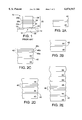
- FIG. 1 represents the relevant portion of a typical flash memory cell 10.
- the memory cell 10 typically includes a source region 12, a drain region 14 and a channel region 16 in a substrate 18; and a stacked gate structure 20 overlying the channel region 16.
- the stacked gate 20 includes a thin gate dielectric layer 22 (commonly referred to as the tunnel oxide) formed on the surface of the substrate 18.
- the stacked gate 20 also includes a polysilicon floating gate 24 which overlies the tunnel oxide 22 and an interpoly dielectric layer 26 which overlies the floating gate 24.
- the interpoly dielectric layer 26 is often a multilayer insulator such as an oxide-nitride-oxide (ONO) layer having two oxide layers 26a and 26b sandwiching a nitride layer 26c.
- a polysilicon control gate 28 overlies the interpoly dielectric layer 26.
- the channel region 16 of the memory cell 10 conducts current between the source region 12 and the drain region 14 in accordance with an electric field developed in the channel region 16 by the stacked gate structure 20.
- a flash memory cell is programmed by inducing hot electron injection from a portion of the substrate, such as the channel section near the drain region, to the floating gate. Electron injection carries negative charge into the floating gate.
- the injection mechanism can be induced by grounding the source region and a bulk portion of the substrate and applying a relatively high positive voltage to the control electrode to create an electron attracting field and applying a positive voltage of moderate magnitude to the drain region in order to generate "hot" (high energy) electrons.
- the negative potential of the floating gate raises the threshold voltage (V th ) of its field effect transistor (FET) and inhibits current flow through the channel region through a subsequent "read" mode.
- the magnitude of the read current is used to determine whether or not a flash memory cell is programmed.
- the act of discharging the floating gate of a flash memory cell is called the erase function.
- the erase function is typically carried out by a Fowler-Nordheim tunneling mechanism between the floating gate and the source region of the transistor (source erase or negative gate erase) or between the floating gate and the substrate (channel erase).
- a source erase operation is induced by applying a high positive voltage to the source region and a 0 V to the control gate and the substrate while floating the drain of the respective memory cell.
- conventional source erase operations for the flash memory cell 10 operate in the following manner.
- the memory cell 10 is programmed by applying a relatively high voltage V G (e.g., approximately 12 volts) to the control gate 28 and a moderately high voltage V D (e.g, approximately 9 volts) to the drain region 14 in order to produce "hot" electrons in the channel region 16 near the drain region 14.
- V G relatively high voltage
- V D moderately high voltage
- the hot electrons accelerate across the tunnel oxide 22 and into the floating gate 24 and become trapped in the floating gate 24 since the floating gate 24 is surrounded by insulators (the interpoly dielectric 26 and the tunnel oxide 22).
- the threshold voltage of the memory cell 10 increases by about 3 to 5 volts. This change in the threshold voltage (and thereby the channel conductance) of the memory cell 10 created by the trapped electrons causes the cell to be programmed.
- a predetermined voltage V G that is greater than the threshold voltage of an unprogrammed cell, but less than the threshold voltage of a programmed cell, is applied to the control gate 28. If the memory cell 10 conducts, then the memory cell 10 has not been programmed (the cell 10 is therefore at a first logic state, e.g., a zero "0"). Likewise, if the memory cell 10 does not conduct, then the memory cell 10 has been programmed (the cell 10 is therefore at a second logic state, e.g., a one "1"). Consequently, it is possible to read each cell 10 to determine whether or not it has been programmed (and therefore identify its logic state).
- V S a relatively high voltage
- V G a ground potential
- the ONO interpoly dielectric layer has a number of important functions including insulating the control gate from the floating gate. Accordingly, it is desirable to form a high quality ONO interpoly dielectric layer.
- ONO interpoly dielectric layer there are a number of concerns. For example, if the top oxide layer is too thick, the required programming voltage increases undesirably. On the other hand, if the top oxide layer is too thin (for example, less than 10 ⁇ ), charge retention time decreases undesirably since the charge tends to leak. Precisely controlling the thickness of the top oxide layer is a notable concern. Moreover, if the nitride layer is too thin, charge leakage from the floating gate to the control gate may be caused, further decreasing charge retention time.
- the top oxide layer of an ONO interpoly dielectric layer is conventionally formed by a high temperature wet oxidation process. Such a process involves oxidizing the nitride layer in steam and oxygen at a temperature of about 950° C. for about 40 minutes. Grown oxides, such as those grown using a wet oxidation process, typically are prone to fewer problems compared with deposited oxides. For example, the undesirable presence of contaminant particles, nonuniform molecular structure, and uneven thickness are problems commonly associated with deposited oxides.
- a number of problems are also associated with forming the top oxide layer using a wet oxidation process.
- One problem is that the process may consume an undesirably large amount of the nitride film. Consequently, the resultant nitride layer is thinned which can cause charge leakage from the floating gate to the control gate.
- Another problem is that the relatively long process time and relatively high temperature may degrade the tunnel oxide. Furthermore, such a process sometimes leads to junction problems at the nitride layer--top oxide layer interface.
- a flash memory cell having improved reliability is obtainable by providing an improved ONO interlayer dielectric layer.
- a top oxide layer having a low defect density and less interface traps despite using a deposition process, charge leakage from the floating gate to the control gate is prevented while Fowler-Nordheim electron tunneling is facilitated.
- forming a top oxide layer in accordance with the present invention does not degrade or deleteriously effect the underlying nitride layer of the ONO interlayer dielectric layer.
- the present invention also makes it possible to precisely control the thickness of the top oxide layer despite using a deposition process.
- Another advantage associated with the present invention is that the nitride layer and the top oxide layer are more compatible thereby minimizing junction problems therebetween.
- the present invention relates to a method of forming a flash memory cell, involving the steps of forming a tunnel oxide on a substrate; forming a first polysilicon layer over the tunnel oxide; forming an insulating layer over the first polysilicon layer, the insulating layer comprising a first oxide layer over the first polysilicon layer, a nitride layer over the first oxide layer, and a second oxide layer over the nitride layer, wherein the second oxide layer is made by forming the second oxide layer by low pressure chemical vapor deposition at a temperature from about 600° C. to about 850° C. using SiH 4 and N 2 O, and annealing in an N 2 O atmosphere at a temperature from about 700° C.
- the present invention relates to a method of forming an ONO insulating layer for a flash memory cell without substantially decreasing nitride layer thickness, involving the steps of depositing a first oxide layer; depositing a nitride layer to a first thickness; and depositing a second oxide layer by low pressure chemical vapor deposition at a temperature from about 600° C. to about 850° C. using SiH 4 and N 2 O, and annealing the second oxide layer in an N 2 O atmosphere at a temperature from about 700° C. to about 950° C., wherein the nitride layer has a second thickness after deposition of the second oxide layer, and the second thickness is at least 95% of the first thickness.
- the present invention relates to a method of decreasing charge leakage from a floating gate to a control gate in a flash memory cell comprising a substrate, a tunnel oxide over the substrate, the floating gate over the tunnel oxide, an ONO insulating layer over the floating gate, and the control gate over the ONO insulating layer, wherein the ONO insulating layer comprises a first oxide layer over the floating gate, a nitride layer over the first oxide layer and a second oxide layer over the nitride layer, involving the steps of forming the second oxide layer by low pressure chemical vapor deposition at a temperature from about 700° C. to about 800° C. using SiH 4 and N 2 O; and annealing in an N 2 O atmosphere at a temperature from about 750° C. to about 900° C.
- FIG. 1 is a cross-sectional view of relevant portions of a conventional memory cell in a flash memory cell.
- FIGS. 2A to 2H are cross-sectional views illustrating a flash memory cell fabrication method according to one embodiment of the present invention.
- the reliability of the interpoly dielectric layer can be increased in flash memory cells. While not wishing to be bound to any theory, it is believed that by forming a top oxide layer according to the present invention, it is consequently possible to prevent charge leakage from the floating gate to the control gate and facilitate Fowler-Nordheim electron tunneling thereby enhancing the erase operation.
- the top oxide layer of an ONO dielectric layer is formed by a two step process.
- the process conditions for forming the top oxide layer involve depositing an oxide by low pressure chemical vapor deposition (LPCVD) followed by a rapid thermal anneal (RTA).
- LPCVD low pressure chemical vapor deposition
- RTA rapid thermal anneal
- Depositing the oxide by LPCVD is conducted at a temperature from about 600° C. to about 850° C. and a pressure from about 400 mTorr to about 750 mTorr. In a preferred embodiment, the temperature is from about 700° C. to about 800° C. and the pressure is from about 500 mTorr to about 700 mTorr.
- the gas flow includes SiH 4 and N 2 O. Although not generally required, the gas flow may optionally include an inert gas such as a noble gas or nitrogen. Nobles gases include He, Ne, Ar, Kr, and Xe. The gas flow generally contains a sufficient amount of SiH 4 and N 2 O to form an oxide layer (an SiO 2 layer). During LPCVD, it is believed that the following chemical reaction takes place.
- the gas flow contains from about 10 standard cubic centimeters per minute (sccm) to about 30 sccm SiH 4 and from about 1 l to about 4 l N 2 O. In another embodiment, the gas flow contains from about 15 sccm to about 25 sccm SiH 4 and from about 1.1 l to about 2 l N 2 O.
- sccm standard cubic centimeters per minute
- the LPCVD is conducted for a time sufficient to form an initial oxide layer of desired thickness wherein the time depends upon the deposition rate.
- the LPCVD deposition rate is from about 3 ⁇ /min to about 6 ⁇ /min.
- the LPCVD deposition rate is from about 3.5 ⁇ /min to about 5.5 ⁇ /min.
- the LPCVD deposition rate is from about 4 ⁇ /min to about 5 ⁇ /min.
- the thickness of the LPCVD oxide is sufficient to provide a resultant top oxide layer (after RTA) having a thickness from about 20 ⁇ to about 80 ⁇ .
- the initial oxide layer (formed by LPCVD in the first step of the two step process) has a thickness from about 20 ⁇ to about 80 ⁇ .
- the initial oxide layer formed by LPCVD has a thickness from about 30 ⁇ to about 60 ⁇ .
- the LPCVD provides an oxide layer having a low defect density without substantially decreasing the thickness or deleteriously effecting the underlying nitride layer.
- the nitride layer after forming the top oxide layer over a nitride layer, retains at least about 95% of its thickness (compared to before LPCVD), and preferably about 100% of its thickness.
- RTA is performed.
- RTA of the oxide layer is preferably conducted in an N 2 O atmosphere.
- An N 2 O atmosphere includes at least about 95% N 2 O (an inert gas constituting any remainder), preferably at least about 99% N 2 O, and more preferably about 100% N 2 O.
- RTA is conducted at a temperature from about 700° C. to about 950° C. In a preferred embodiment, RTA is conducted at a temperature from about 750° C. to about 900° C.
- RTA is conducted for a time from about 40 seconds to about 80 seconds. In a preferred embodiment, RTA is conducted for a time from about 50 seconds to about 70 seconds.
- the RTA serves to decrease the defect density of the oxide layer.
- the RTA also serves to reduce charge trapping in the top oxide layer of the completed flash memory cell. It is believed that at elevated temperatures, N 2 O dissociates into nitrogen gas (N 2 ) and reactive atomic oxygen. It is also believed that the reactive atomic oxygen diffuses into the LPCVD oxide layer repairing oxygen vacancies, thereby reducing the defect density and leakage current.
- the thickness of the resultant top oxide layer formed in accordance with the invention is from about 20 ⁇ to about 80 ⁇ . In another embodiment, the thickness of the resultant top oxide layer formed in accordance with the invention is from about 30 ⁇ to about 60 ⁇ .
- the resultant top oxide layer has a substantially uniform thickness and a low defect density.
- a plurality of flash memory cells can be formed on a semiconductor substrate, such as a silicon die, each with an N-type source region and N-type drain region formed within a P portion of the substrate and a P-type channel region interposed between the source and drain regions in accordance with the present invention.
- a semiconductor substrate such as a silicon die
- N-type source region and N-type drain region formed within a P portion of the substrate and a P-type channel region interposed between the source and drain regions in accordance with the present invention.
- a P-type substrate 40 is provided. Thereafter, a thin tunnel oxide layer 42 is formed over the substrate 40 having a thickness of, for example, about 50 ⁇ to about 150 ⁇ using a thermal growth process in a dry oxidation furnace.
- the tunnel oxide layer 42 can be formed via dry oxidation at a temperature of about 1050° C., under an atmosphere of oxygen at about 1.33 l, HCl at about 70 cc and argon at about 12.61.
- the tunnel oxide can be formed from oxynitride.
- a phosphorus doped polysilicon layer is deposited via CVD to form a doped polysilicon layer 44 at 530° C., 400 mTorr, SiH 4 at 2000 sccm, and a mixture of 1% by weight PH 3 in helium at about 22 sccm. Doping lowers the resistivity of the polysilicon rendering it conductive.
- a multi-layer interpoly dielectric 46 is then formed over the surface of the substrate 40, as illustrated in FIG. 2C.
- This layer 46 is often called the interpoly dielectric since (as will be seen shortly) it is sandwiched between the phosphorus doped polysilicon layer (first polysilicon layer constituting the floating gate for a flash memory cell) and a second polysilicon layer which forms the control gate for the cell.
- the interpoly dielectric 46 is preferably a three layer region of oxide/nitride/oxide (a so called "ONO" layer) and typically has a total thickness of about 120 ⁇ to about 400 ⁇ .
- the ONO layer 46 is formed by repetitive depositions of oxide, nitride and oxide to form a dielectric layer in which the nitride is sandwiched between a bottom oxide layer and top oxide layer.
- a first or bottom oxide layer 46a is deposited using CVD techniques.
- a bottom oxide layer 46a is deposited at a temperature of about 750° C. under SiH 4 at 20 sccm, N 2 O at 1.2 l, and a carrier gas and a pressure of 600 mTorr via LPCVD oxide on the first polysilicon layer.
- the bottom oxide layer may have a suitable thickness, for example, from about 40 ⁇ to about 60 ⁇ , but typically the thickness is about 50 ⁇ .
- a nitride layer 46b is next deposited also using CVD techniques. For example, nitride is deposited at a temperature of about 760° C.
- the nitride layer 46b may have a suitable thickness, for example, from about 60 ⁇ to about 100 ⁇ , preferably from about 70 ⁇ to about 90 ⁇ , but typically the thickness is about 80 ⁇ .
- the second or top oxide layer 46c is formed by initially performing LPCVD at a temperature of about 750° C. and a pressure of about 600 mTorr using a gas flow containing about 1.2 l N 2 O and about 20 sccm SiH 4 for about 9 minutes to provide an LPCVD initial oxide layer having a thickness of about 40 ⁇ .
- RTA of the LPCVD oxide layer is conducted in an N 2 O atmosphere at a temperature of about 800° C. for about 60 seconds.
- the top oxide layer may have a thickness from about 20 ⁇ to about 80 ⁇ , but in this embodiment about 40 ⁇ .
- the thickness of the underlying nitride layer 46b does not substantially decrease during formation of the top oxide layer 46c.
- the nitride layer 46b is deposited at a thickness of 80 ⁇ , after formation of the top oxide layer 46c, the nitride layer 46b has a thickness of at least about 76 ⁇ . In this embodiment, the thickness of the nitride layer 46b is about 80 ⁇ . Also as a result of the conditions used to form the top oxide layer 46c, it is possible to precisely control the thickness of the top oxide layer.
- the second polysilicon layer is deposited.
- a phosphorus doped amorphous polysilicon layer is deposited via CVD to form a doped polysilicon layer 48 at about 530° C., 400 mTorr, SiH 4 at 2,000 sccm, and a mixture of 1% by weight PH 3 in helium at about 75 sccm.
- the second polysilicon layer can be deposited by LPCVD followed by ion implantation of a dopant such as phosphorus. Doping lowers the resistivity of the polysilicon rendering it conductive.
- a tungsten silicide layer 50 is deposited via, for example, LPCVD.
- the tungsten silicide layer 50 provides a lower resistance contact for improved flash memory cell performance.
- Poly-cap layer 52 is deposited over the tungsten silicide layer 50.
- the poly-cap layer 52 is about 500 ⁇ thick, and is formed via, for example, LPCVD.
- the poly-cap layer 52 can be used to prevent any potential peeling or cracking of the underlying tungsten silicide 50.
- a capping layer 54, for example, of SiON is deposited over the poly-cap layer 52.
- the capping silicon oxynitride layer 54 provides an anti-reflective coating at masking and also acts as a masking layer for subsequent etching.
- etching is performed to define one or more pre-stack structures.
- the etching may be achieved by depositing and defining a photoresist masking layer over the entire surface of the substrate using standard lithography procedures. This is generally termed the gate mask and gate etch.
- a number of successive etching steps such as the gate etch and the self aligned etch, are performed to define one or more stack structures 56. This is generally termed the self aligned mask and self aligned etch.
- the gate mask and gate etch are performed as follows. First, a resist (not shown) is applied, selectively exposed to radiation and developed whereby various portions removed (either the exposed or unexposed portions). Next, in one embodiment, the etching steps take place in a multi-chamber etch tool wherein a silicon oxynitride capping layer is selectively etched with a fluorinated chemistry such as CHF 3 --O 2 in an oxide chamber. The exposed poly-cap layer and the tungsten silicide layer are then etched with SF 6 /HBr (or alternatively, SF 6 /Cl 2 or Cl 2 --O 2 ) and the exposed second polysilicon layer is etched with HBr--O 2 in a poly chamber. Etching steps are preferably formed in an integrated process in which the wafers are not exposed to atmosphere when transferring the wafers from one chamber to another.
- a self aligned etch (“SAE") is performed to remove the ONO layer 46 and the phosphorus doped polysilicon layer (first polysilicon layer) 44 in the regions that are not covered by the pre-stack structure (constituted by the unremoved second polysilicon layer, tungsten silicide layer, poly-cap layer and capping layer).
- the SAE etch is a two step etch process in which the ONO layer 46 is first removed using, for example, a CF 4 --O 2 RIE etch, The second phase of the SAE etch is the removal of the exposed first polysilicon layer 44 to thereby further define the floating gate structures for each respective word line.
- the polysilicon etch includes, for example, an HBr--O 2 or a HBr--Cl 2 --O 2 RIE etch chemistry.
- the gate etch and SAE serve to define the stack structure 56.
- the fabrication of the flash memory cells is then completed by forming the source and drain regions by, for example, ion implantation.
- the stacked gate structure 56 serves as a self-aligning mechanism.
- resist 62 is applied and selectively stripped followed by performing a first ion implantation using phosphorus (1 ⁇ 10 14 ions/cm 2 at 60 KeV) to form an N-type source region 64 (double diffused implant).
- resist 62 is removed followed by performing a second ion implantation using arsenic (5 ⁇ 10 14 ions/cm 2 at 40 KeV) to form deep N-type source region 66, shallow N-type source region 68 and N-type drain region 70 (modified drain diffusion). Annealing completes the formation of the source and drain regions.
- arsenic 5 ⁇ 10 14 ions/cm 2 at 40 KeV
- Annealing completes the formation of the source and drain regions.
- the source regions 66 and 68 and the substrate 40 of the memory cell may be tied to a ground via a terminal (not shown), respectively, the drain region 70 is. coupled to a relatively high voltage (for example, between about +5 V to about +9 V) via a terminal (not shown) and the control gate 48 is connected to a relatively high voltage level (for example, above about +10 V) via a terminal (not shown). Electrons are accelerated from the source regions 66 and 68 to the drain region 70 and so-called "hot-electrons" are generated near the drain region 70. Some of the hot electrons are injected through the relatively thin tunnel oxide layer 42 and become trapped in the floating gate 44 thereby providing the floating gate 44 with a negative potential.
- a relatively high voltage for example, between about +5 V to about +9 V
- the control gate 48 is connected to a relatively high voltage level (for example, above about +10 V) via a terminal (not shown). Electrons are accelerated from the source regions 66 and 68 to the drain region 70 and so-
- a high positive voltage (such as above about +12 V) is applied to the source regions 66 and 68 via a source terminal (not shown).
- a ground potential (V g equals 0 V) is applied to the control gate 48 via the control terminal (not shown).
- a similar ground potential (V sub equals 0 V) is applied to the substrate 40 via a substrate terminal (not shown).
- V D of the drain region 70 is permitted to float.
- electrons previously stored during programming in the floating gate 44 pass through tunnel oxide layer 42 by way of Fowler-Nordheim tunneling and travel into the source regions 66 and 68 as a result of the electric field established between the control gate 48 and the source regions 66 and 68 (V GS equals about 12 V). Since the top oxide layer is characterized by reduced charge trapping, Fowler-Nordheim tunneling and travel of electrons from the floating gate 44 to the source regions 66 and 68 are facilitated.
Landscapes
- Semiconductor Memories (AREA)
- Non-Volatile Memory (AREA)
Abstract
Description
SiH.sub.4 +4N.sub.2 O→SiO.sub.2 +2H.sub.2 O+4N.sub.2
Claims (20)
Priority Applications (1)
| Application Number | Priority Date | Filing Date | Title |
|---|---|---|---|
| US09/189,227 US6074917A (en) | 1998-06-16 | 1998-11-11 | LPCVD oxide and RTA for top oxide of ONO film to improve reliability for flash memory devices |
Applications Claiming Priority (2)
| Application Number | Priority Date | Filing Date | Title |
|---|---|---|---|
| US09/098,292 US6063666A (en) | 1998-06-16 | 1998-06-16 | RTCVD oxide and N2 O anneal for top oxide of ONO film |
| US09/189,227 US6074917A (en) | 1998-06-16 | 1998-11-11 | LPCVD oxide and RTA for top oxide of ONO film to improve reliability for flash memory devices |
Related Parent Applications (1)
| Application Number | Title | Priority Date | Filing Date |
|---|---|---|---|
| US09/098,292 Continuation-In-Part US6063666A (en) | 1998-06-16 | 1998-06-16 | RTCVD oxide and N2 O anneal for top oxide of ONO film |
Publications (1)
| Publication Number | Publication Date |
|---|---|
| US6074917A true US6074917A (en) | 2000-06-13 |
Family
ID=46255254
Family Applications (1)
| Application Number | Title | Priority Date | Filing Date |
|---|---|---|---|
| US09/189,227 Expired - Lifetime US6074917A (en) | 1998-06-16 | 1998-11-11 | LPCVD oxide and RTA for top oxide of ONO film to improve reliability for flash memory devices |
Country Status (1)
| Country | Link |
|---|---|
| US (1) | US6074917A (en) |
Cited By (69)
| Publication number | Priority date | Publication date | Assignee | Title |
|---|---|---|---|---|
| US6146929A (en) * | 1998-07-09 | 2000-11-14 | Kabushiki Kaisha Toshiba | Method for manufacturing semiconductor device using multiple steps continuously without exposing substrate to the atmosphere |
| US6162684A (en) * | 1999-03-11 | 2000-12-19 | Advanced Micro Devices, Inc. | Ammonia annealed and wet oxidized LPCVD oxide to replace ono films for high integrated flash memory devices |
| US6265268B1 (en) * | 1999-10-25 | 2001-07-24 | Advanced Micro Devices, Inc. | High temperature oxide deposition process for fabricating an ONO floating-gate electrode in a two bit EEPROM device |
| US6319775B1 (en) * | 1999-10-25 | 2001-11-20 | Advanced Micro Devices, Inc. | Nitridation process for fabricating an ONO floating-gate electrode in a two-bit EEPROM device |
| US6368919B2 (en) * | 1999-01-19 | 2002-04-09 | Micron Technology, Inc. | Method and composite for decreasing charge leakage |
| US6376308B1 (en) * | 2000-01-19 | 2002-04-23 | Advanced Micro Devices, Inc. | Process for fabricating an EEPROM device having a pocket substrate region |
| US20020117731A1 (en) * | 2001-02-23 | 2002-08-29 | Samsung Electronics Co., Ltd. | Method for forming layer for trench isolation structure |
| US6458677B1 (en) * | 1999-10-25 | 2002-10-01 | Advanced Micro Devices, Inc. | Process for fabricating an ONO structure |
| US6537881B1 (en) * | 2000-10-16 | 2003-03-25 | Advanced Micro Devices, Inc. | Process for fabricating a non-volatile memory device |
| US20030071304A1 (en) * | 1999-08-13 | 2003-04-17 | Ogle Robert B. | Method of forming flash memory having pre-interpoly dielectric treatment layer |
| US6709927B1 (en) * | 2000-08-11 | 2004-03-23 | Advanced Micro Devices, Inc. | Process for treating ONO dielectric film of a floating gate memory cell |
| US20040229350A1 (en) * | 2003-05-12 | 2004-11-18 | Nikolai Strelchenko | Morula derived embryonic stem cells |
| US20040228969A1 (en) * | 2003-05-16 | 2004-11-18 | Macronix International Co., Ltd. | Method for forming ONO top oxide in NROM structure |
| US20050110102A1 (en) * | 2003-11-25 | 2005-05-26 | Macronix International Co., Ltd. | Method for forming oxide on ONO structure |
| US20050162922A1 (en) * | 2004-01-27 | 2005-07-28 | Macronix International Co., Ltd. | Circuit and method for programming charge storage memory cells |
| US20050219906A1 (en) * | 2004-01-27 | 2005-10-06 | Macronix International Co., Ltd. | Operation scheme for programming charge trapping non-volatile memory |
| US20050237801A1 (en) * | 2004-04-26 | 2005-10-27 | Macronix International Co., Ltd. | Operation scheme with charge balancing for charge trapping non-volatile memory |
| US20050237813A1 (en) * | 2004-04-26 | 2005-10-27 | Macronix International Co., Ltd. | Method and system for self-convergent erase in charge trapping memory cells |
| US20050237815A1 (en) * | 2004-04-26 | 2005-10-27 | Macronix International Co., Ltd. | Operation scheme with charge balancing erase for charge trapping non-volatile memory |
| US20050237809A1 (en) * | 2004-04-26 | 2005-10-27 | Macronix International Co., Ltd. | Operation scheme with high work function gate and charge balancing for charge trapping non-volatile memory |
| US20050237816A1 (en) * | 2004-04-26 | 2005-10-27 | Macronix International Co., Ltd. | Operation scheme for spectrum shift in charge trapping non-volatile memory |
| US20050281085A1 (en) * | 2004-06-17 | 2005-12-22 | Macronix International Co., Ltd. | Operation scheme for programming charge trapping non-volatile memory |
| US20060007741A1 (en) * | 2004-07-06 | 2006-01-12 | Macronix International Co., Ltd. | Charge trapping non-volatile memory with two trapping locations per gate, and method for operating same |
| US20060007732A1 (en) * | 2004-07-06 | 2006-01-12 | Macronix International Co., Ltd. | Charge trapping non-volatile memory and method for operating same |
| US7001814B1 (en) | 2003-05-16 | 2006-02-21 | Advanced Micro Devices, Inc. | Laser thermal annealing methods for flash memory devices |
| US20060109717A1 (en) * | 2004-11-19 | 2006-05-25 | Macronix International Co., Ltd. | Method and apparatus for programming nonvolatile memory |
| US20060198190A1 (en) * | 2005-01-03 | 2006-09-07 | Macronix International Co., Ltd. | Non-volatile memory cells, memory arrays including the same and methods of operating cells and arrays |
| US20060198189A1 (en) * | 2005-01-03 | 2006-09-07 | Macronix International Co., Ltd. | Non-volatile memory cells, memory arrays including the same and methods of operating cells and arrays |
| US20060202261A1 (en) * | 2005-01-03 | 2006-09-14 | Macronix International Co., Ltd. | Non-volatile memory cells, memory arrays including the same and methods of operating cells and arrays |
| US20060202252A1 (en) * | 2005-01-03 | 2006-09-14 | Macronix International Co., Ltd. | Non-volatile memory cells, memory arrays including the same and methods of operating cells and arrays |
| US20060245246A1 (en) * | 2005-04-29 | 2006-11-02 | Macronix International Co., Ltd. | Inversion bit line, charge trapping non-volatile memory and method of operating same |
| US20060244046A1 (en) * | 1998-12-09 | 2006-11-02 | Kabushiki Kaisha Toshiba | Non-Volatile Semiconductor Memory Device |
| US20060270157A1 (en) * | 2005-05-30 | 2006-11-30 | Hynix Semiconductor Inc. | Method of manufacturing flash memory device |
| US20060281260A1 (en) * | 2005-06-10 | 2006-12-14 | Hang-Ting Lue | Methods of operating p-channel non-volatile memory devices |
| US20060281331A1 (en) * | 2004-11-29 | 2006-12-14 | Macronix International Co., Ltd. | Charge trapping dielectric structure for non-volatile memory |
| US20060292794A1 (en) * | 2005-06-24 | 2006-12-28 | Hynix Semiconductor Inc. | Method of manufacturing dielectric film of flash memory device |
| US20070029625A1 (en) * | 2005-08-04 | 2007-02-08 | Macronix International Co., Ltd. | Non-volatile memory semiconductor device having an oxide-nitride-oxide (ONO) top dielectric layer |
| US20070054449A1 (en) * | 2005-08-23 | 2007-03-08 | Macronix International Co. Ltd. | Methods of forming charge-trapping dielectric layers for semiconductor memory devices |
| US20070134876A1 (en) * | 2005-12-09 | 2007-06-14 | Macronix International Co., Ltd. | Stacked thin film transistor, non-volatile memory devices and methods for fabricating the same |
| US20070134855A1 (en) * | 2005-12-09 | 2007-06-14 | Macronix International Co., Ltd. | A stacked non-volatile memory device and methods for fabricating the same |
| US20070138539A1 (en) * | 2005-12-15 | 2007-06-21 | Macronix International Co., Ltd. | Non-volatile memory device having a nitride-oxide dielectric layer |
| US20070258291A1 (en) * | 2006-05-08 | 2007-11-08 | Macronix International Co., Ltd. | Methods and apparatus for implementing bit-by-bit erase of a flash memory device |
| US20070284620A1 (en) * | 2006-05-23 | 2007-12-13 | Macronix International Co., Ltd. | Structure and Method of Sub-Gate and Architectures Employing Bandgap Engineered SONOS Devices |
| US20070290273A1 (en) * | 2006-06-20 | 2007-12-20 | Macronix International Co., Ltd. | Operating method of non-volatile memory device |
| US20080087946A1 (en) * | 2006-10-11 | 2008-04-17 | Macronix International Co., Ltd. | Vertical channel transistor structure and manufacturing method thereof |
| US20080116506A1 (en) * | 2006-11-20 | 2008-05-22 | Macronix International Co., Ltd. | Charge trapping devices with field distribution layer over tunneling barrier |
| US20090039416A1 (en) * | 2007-08-09 | 2009-02-12 | Macronix International Co., Ltd. | Blocking dielectric engineered charge trapping memory cell with high speed erase |
| US20090059676A1 (en) * | 2007-08-27 | 2009-03-05 | Macronix International Co., Ltd. | HIGH-k CAPPED BLOCKING DIELECTRIC BANDGAP ENGINEERED SONOS AND MONOS |
| US20090103367A1 (en) * | 2007-10-18 | 2009-04-23 | Macronix International Co., Ltd. | One-transistor cell semiconductor on insulator random access memory |
| US20090103370A1 (en) * | 2007-10-18 | 2009-04-23 | Macronix International Co., Ltd. | Efficient erase algorithm for sonos-type nand flash |
| US20090141555A1 (en) * | 2006-05-05 | 2009-06-04 | Macronix International Co., Ltd. | Method of programming and erasing a p-channel be-sonos nand flash memory |
| US20090175089A1 (en) * | 2008-01-08 | 2009-07-09 | Boaz Eitan | Retention in NVM with top or bottom injection |
| US20090262583A1 (en) * | 2008-04-18 | 2009-10-22 | Macronix International Co., Ltd. | Floating gate memory device with interpoly charge trapping structure |
| US20100172183A1 (en) * | 2009-01-02 | 2010-07-08 | Macronix International Co., Ltd. | Method and Apparatus to Suppress Fringing Field Interference of Charge Trapping NAND Memory |
| US7772068B2 (en) | 2006-08-30 | 2010-08-10 | Macronix International Co., Ltd. | Method of manufacturing non-volatile memory |
| US20100227466A1 (en) * | 2006-07-10 | 2010-09-09 | Macronix International Co., Ltd. | Nonvolatile Memory Array Having Modified Channel Region Interface |
| US20100265766A1 (en) * | 2009-04-21 | 2010-10-21 | Macronix International Co., Ltd. | Bandgap engineered charge trapping memory in two-transistor nor architecture |
| US7838923B2 (en) | 2007-08-09 | 2010-11-23 | Macronix International Co., Ltd. | Lateral pocket implant charge trapping devices |
| US7851848B2 (en) | 2006-11-01 | 2010-12-14 | Macronix International Co., Ltd. | Cylindrical channel charge trapping devices with effectively high coupling ratios |
| US7948799B2 (en) | 2006-05-23 | 2011-05-24 | Macronix International Co., Ltd. | Structure and method of sub-gate NAND memory with bandgap engineered SONOS devices |
| US8223540B2 (en) | 2007-02-02 | 2012-07-17 | Macronix International Co., Ltd. | Method and apparatus for double-sided biasing of nonvolatile memory |
| US8482052B2 (en) | 2005-01-03 | 2013-07-09 | Macronix International Co., Ltd. | Silicon on insulator and thin film transistor bandgap engineered split gate memory |
| US8772858B2 (en) | 2006-10-11 | 2014-07-08 | Macronix International Co., Ltd. | Vertical channel memory and manufacturing method thereof and operating method using the same |
| US8987098B2 (en) | 2012-06-19 | 2015-03-24 | Macronix International Co., Ltd. | Damascene word line |
| US9099538B2 (en) | 2013-09-17 | 2015-08-04 | Macronix International Co., Ltd. | Conductor with a plurality of vertical extensions for a 3D device |
| US9240405B2 (en) | 2011-04-19 | 2016-01-19 | Macronix International Co., Ltd. | Memory with off-chip controller |
| US9379126B2 (en) | 2013-03-14 | 2016-06-28 | Macronix International Co., Ltd. | Damascene conductor for a 3D device |
| US9559113B2 (en) | 2014-05-01 | 2017-01-31 | Macronix International Co., Ltd. | SSL/GSL gate oxide in 3D vertical channel NAND |
| CN112106173A (en) * | 2018-07-31 | 2020-12-18 | 应用材料公司 | CVD-based spacer deposition with zero loading |
Citations (11)
| Publication number | Priority date | Publication date | Assignee | Title |
|---|---|---|---|---|
| US4698787A (en) * | 1984-11-21 | 1987-10-06 | Exel Microelectronics, Inc. | Single transistor electrically programmable memory device and method |
| US5231299A (en) * | 1992-03-24 | 1993-07-27 | International Business Machines Corporation | Structure and fabrication method for EEPROM memory cell with selective channel implants |
| US5397720A (en) * | 1994-01-07 | 1995-03-14 | The Regents Of The University Of Texas System | Method of making MOS transistor having improved oxynitride dielectric |
| US5420060A (en) * | 1988-11-14 | 1995-05-30 | Texas Instruments Incorporated | Method of making contract-free floating-gate memory array with silicided buried bitlines and with single-step defined floating gates |
| US5457336A (en) * | 1994-10-13 | 1995-10-10 | Advanced Micro Devices, Inc. | Non-volatile memory structure including protection and structure for maintaining threshold stability |
| US5467308A (en) * | 1994-04-05 | 1995-11-14 | Motorola Inc. | Cross-point eeprom memory array |
| US5496756A (en) * | 1994-04-29 | 1996-03-05 | Motorola Inc. | Method for forming a nonvolatile memory device |
| US5512505A (en) * | 1990-12-18 | 1996-04-30 | Sandisk Corporation | Method of making dense vertical programmable read only memory cell structure |
| US5591681A (en) * | 1994-06-03 | 1997-01-07 | Advanced Micro Devices, Inc. | Method for achieving a highly reliable oxide film |
| US5654217A (en) * | 1994-05-25 | 1997-08-05 | Sandisk Corporation | Dense flash EEPROM cell array and peripheral supporting circuits formed in deposited field oxide with the use of spacers |
| US5674788A (en) * | 1995-06-06 | 1997-10-07 | Advanced Micro Devices, Inc. | Method of forming high pressure silicon oxynitride gate dielectrics |
-
1998
- 1998-11-11 US US09/189,227 patent/US6074917A/en not_active Expired - Lifetime
Patent Citations (12)
| Publication number | Priority date | Publication date | Assignee | Title |
|---|---|---|---|---|
| US4698787A (en) * | 1984-11-21 | 1987-10-06 | Exel Microelectronics, Inc. | Single transistor electrically programmable memory device and method |
| US5420060A (en) * | 1988-11-14 | 1995-05-30 | Texas Instruments Incorporated | Method of making contract-free floating-gate memory array with silicided buried bitlines and with single-step defined floating gates |
| US5512505A (en) * | 1990-12-18 | 1996-04-30 | Sandisk Corporation | Method of making dense vertical programmable read only memory cell structure |
| US5231299A (en) * | 1992-03-24 | 1993-07-27 | International Business Machines Corporation | Structure and fabrication method for EEPROM memory cell with selective channel implants |
| US5397720A (en) * | 1994-01-07 | 1995-03-14 | The Regents Of The University Of Texas System | Method of making MOS transistor having improved oxynitride dielectric |
| US5541436A (en) * | 1994-01-07 | 1996-07-30 | The Regents Of The University Of Texas System | MOS transistor having improved oxynitride dielectric |
| US5467308A (en) * | 1994-04-05 | 1995-11-14 | Motorola Inc. | Cross-point eeprom memory array |
| US5496756A (en) * | 1994-04-29 | 1996-03-05 | Motorola Inc. | Method for forming a nonvolatile memory device |
| US5654217A (en) * | 1994-05-25 | 1997-08-05 | Sandisk Corporation | Dense flash EEPROM cell array and peripheral supporting circuits formed in deposited field oxide with the use of spacers |
| US5591681A (en) * | 1994-06-03 | 1997-01-07 | Advanced Micro Devices, Inc. | Method for achieving a highly reliable oxide film |
| US5457336A (en) * | 1994-10-13 | 1995-10-10 | Advanced Micro Devices, Inc. | Non-volatile memory structure including protection and structure for maintaining threshold stability |
| US5674788A (en) * | 1995-06-06 | 1997-10-07 | Advanced Micro Devices, Inc. | Method of forming high pressure silicon oxynitride gate dielectrics |
Non-Patent Citations (4)
| Title |
|---|
| Olivo et al. Charge Trapping and Retention in Ultra Thin ONOStructures, Solid State Electronics, 1991. * |
| Olivo et al. Charge Trapping and Retention in Ultra-Thin ONOStructures, Solid State Electronics, 1991. |
| Olivo, P., Z.A. Weinberg, K.J. Stein and D.S. Wen, "Charge Trapping And Retention In Ultra-Thin Oxide-Nitride-Oxide Structures", Solid State Electronics, vol. 34, No. 6, pp. 609-611, 1991, no month. |
| Olivo, P., Z.A. Weinberg, K.J. Stein and D.S. Wen, Charge Trapping And Retention In Ultra Thin Oxide Nitride Oxide Structures , Solid State Electronics, vol. 34, No. 6, pp. 609 611, 1991, no month. * |
Cited By (165)
| Publication number | Priority date | Publication date | Assignee | Title |
|---|---|---|---|---|
| US6372083B1 (en) | 1998-07-09 | 2002-04-16 | Kabushiki Kaisha Toshiba | Method of manufacturing semiconductor device and apparatus for manufacturing the same |
| US6146929A (en) * | 1998-07-09 | 2000-11-14 | Kabushiki Kaisha Toshiba | Method for manufacturing semiconductor device using multiple steps continuously without exposing substrate to the atmosphere |
| US20060244046A1 (en) * | 1998-12-09 | 2006-11-02 | Kabushiki Kaisha Toshiba | Non-Volatile Semiconductor Memory Device |
| US20060249780A1 (en) * | 1998-12-09 | 2006-11-09 | Kabushiki Kaisha Toshiba. | Non-Volatile Semiconductor Memory Device |
| US20060249781A1 (en) * | 1998-12-09 | 2006-11-09 | Kabushiki Kaisha Toshiba | Non-Volatile Semiconductor Memory Device |
| US6521945B2 (en) | 1999-01-19 | 2003-02-18 | Micron Technology, Inc. | Method and composite for decreasing charge leakage |
| US6746922B2 (en) | 1999-01-19 | 2004-06-08 | Micron Technology, Inc. | Method and composite for decreasing charge leakage |
| US20020093063A1 (en) * | 1999-01-19 | 2002-07-18 | Micron Technology, Inc. | Method and composite for decreasing charge leakage |
| US6368919B2 (en) * | 1999-01-19 | 2002-04-09 | Micron Technology, Inc. | Method and composite for decreasing charge leakage |
| US7087490B2 (en) | 1999-01-19 | 2006-08-08 | Micron Technology, Inc. | Method and composite for decreasing charge leakage |
| US20050026370A1 (en) * | 1999-01-19 | 2005-02-03 | Micron Technology, Inc. | Method and composite for decreasing charge leakage |
| US6803280B2 (en) | 1999-01-19 | 2004-10-12 | Micron Technology, Inc. | Method and composite for decreasing charge leakage |
| US6791148B2 (en) | 1999-01-19 | 2004-09-14 | Micron Technology, Inc. | Method and composite for decreasing charge leakage |
| US6162684A (en) * | 1999-03-11 | 2000-12-19 | Advanced Micro Devices, Inc. | Ammonia annealed and wet oxidized LPCVD oxide to replace ono films for high integrated flash memory devices |
| US6716702B2 (en) * | 1999-08-13 | 2004-04-06 | Advanced Micro Devices, Inc. | Method of forming flash memory having pre-interpoly dielectric treatment layer |
| US20030071304A1 (en) * | 1999-08-13 | 2003-04-17 | Ogle Robert B. | Method of forming flash memory having pre-interpoly dielectric treatment layer |
| US6319775B1 (en) * | 1999-10-25 | 2001-11-20 | Advanced Micro Devices, Inc. | Nitridation process for fabricating an ONO floating-gate electrode in a two-bit EEPROM device |
| US6265268B1 (en) * | 1999-10-25 | 2001-07-24 | Advanced Micro Devices, Inc. | High temperature oxide deposition process for fabricating an ONO floating-gate electrode in a two bit EEPROM device |
| US6458677B1 (en) * | 1999-10-25 | 2002-10-01 | Advanced Micro Devices, Inc. | Process for fabricating an ONO structure |
| US6376308B1 (en) * | 2000-01-19 | 2002-04-23 | Advanced Micro Devices, Inc. | Process for fabricating an EEPROM device having a pocket substrate region |
| US6709927B1 (en) * | 2000-08-11 | 2004-03-23 | Advanced Micro Devices, Inc. | Process for treating ONO dielectric film of a floating gate memory cell |
| US6537881B1 (en) * | 2000-10-16 | 2003-03-25 | Advanced Micro Devices, Inc. | Process for fabricating a non-volatile memory device |
| US7714325B2 (en) | 2001-02-23 | 2010-05-11 | Samsung Electronics Co., Ltd. | Trench isolation structure |
| US20020117731A1 (en) * | 2001-02-23 | 2002-08-29 | Samsung Electronics Co., Ltd. | Method for forming layer for trench isolation structure |
| US20070210305A1 (en) * | 2001-02-23 | 2007-09-13 | Samsung Electronics Co., Ltd. | Method for forming layer for trench isolation structure |
| US7387943B2 (en) * | 2001-02-23 | 2008-06-17 | Samsung Electronics Co., Ltd. | Method for forming layer for trench isolation structure |
| US20040229350A1 (en) * | 2003-05-12 | 2004-11-18 | Nikolai Strelchenko | Morula derived embryonic stem cells |
| US6962728B2 (en) | 2003-05-16 | 2005-11-08 | Macronix International Co., Ltd. | Method for forming ONO top oxide in NROM structure |
| US20040228969A1 (en) * | 2003-05-16 | 2004-11-18 | Macronix International Co., Ltd. | Method for forming ONO top oxide in NROM structure |
| US7001814B1 (en) | 2003-05-16 | 2006-02-21 | Advanced Micro Devices, Inc. | Laser thermal annealing methods for flash memory devices |
| US20050110102A1 (en) * | 2003-11-25 | 2005-05-26 | Macronix International Co., Ltd. | Method for forming oxide on ONO structure |
| US7919372B2 (en) | 2003-11-25 | 2011-04-05 | Macronix International, Co. Ltd. | Method for forming oxide on ONO structure |
| US7183166B2 (en) | 2003-11-25 | 2007-02-27 | Macronix International Co., Ltd. | Method for forming oxide on ONO structure |
| US20070117353A1 (en) * | 2003-11-25 | 2007-05-24 | Macronix International Co., Ltd. | Method for Forming Oxide on Ono Structure |
| US20050162922A1 (en) * | 2004-01-27 | 2005-07-28 | Macronix International Co., Ltd. | Circuit and method for programming charge storage memory cells |
| US6937511B2 (en) | 2004-01-27 | 2005-08-30 | Macronix International Co., Ltd. | Circuit and method for programming charge storage memory cells |
| US20050219906A1 (en) * | 2004-01-27 | 2005-10-06 | Macronix International Co., Ltd. | Operation scheme for programming charge trapping non-volatile memory |
| US7151692B2 (en) | 2004-01-27 | 2006-12-19 | Macronix International Co., Ltd. | Operation scheme for programming charge trapping non-volatile memory |
| US20050237816A1 (en) * | 2004-04-26 | 2005-10-27 | Macronix International Co., Ltd. | Operation scheme for spectrum shift in charge trapping non-volatile memory |
| US7164603B2 (en) | 2004-04-26 | 2007-01-16 | Yen-Hao Shih | Operation scheme with high work function gate and charge balancing for charge trapping non-volatile memory |
| US7187590B2 (en) | 2004-04-26 | 2007-03-06 | Macronix International Co., Ltd. | Method and system for self-convergent erase in charge trapping memory cells |
| US7209390B2 (en) | 2004-04-26 | 2007-04-24 | Macronix International Co., Ltd. | Operation scheme for spectrum shift in charge trapping non-volatile memory |
| US20050237809A1 (en) * | 2004-04-26 | 2005-10-27 | Macronix International Co., Ltd. | Operation scheme with high work function gate and charge balancing for charge trapping non-volatile memory |
| US20050237815A1 (en) * | 2004-04-26 | 2005-10-27 | Macronix International Co., Ltd. | Operation scheme with charge balancing erase for charge trapping non-volatile memory |
| US20050237813A1 (en) * | 2004-04-26 | 2005-10-27 | Macronix International Co., Ltd. | Method and system for self-convergent erase in charge trapping memory cells |
| US7133313B2 (en) | 2004-04-26 | 2006-11-07 | Macronix International Co., Ltd. | Operation scheme with charge balancing for charge trapping non-volatile memory |
| US20050237801A1 (en) * | 2004-04-26 | 2005-10-27 | Macronix International Co., Ltd. | Operation scheme with charge balancing for charge trapping non-volatile memory |
| US7075828B2 (en) | 2004-04-26 | 2006-07-11 | Macronix International Co., Intl. | Operation scheme with charge balancing erase for charge trapping non-volatile memory |
| US20050281085A1 (en) * | 2004-06-17 | 2005-12-22 | Macronix International Co., Ltd. | Operation scheme for programming charge trapping non-volatile memory |
| US7190614B2 (en) | 2004-06-17 | 2007-03-13 | Macronix International Co., Ltd. | Operation scheme for programming charge trapping non-volatile memory |
| US7106625B2 (en) | 2004-07-06 | 2006-09-12 | Macronix International Co, Td | Charge trapping non-volatile memory with two trapping locations per gate, and method for operating same |
| US20060007732A1 (en) * | 2004-07-06 | 2006-01-12 | Macronix International Co., Ltd. | Charge trapping non-volatile memory and method for operating same |
| US20060007741A1 (en) * | 2004-07-06 | 2006-01-12 | Macronix International Co., Ltd. | Charge trapping non-volatile memory with two trapping locations per gate, and method for operating same |
| US7133317B2 (en) | 2004-11-19 | 2006-11-07 | Macronix International Co., Ltd. | Method and apparatus for programming nonvolatile memory |
| US20060109717A1 (en) * | 2004-11-19 | 2006-05-25 | Macronix International Co., Ltd. | Method and apparatus for programming nonvolatile memory |
| US20060281331A1 (en) * | 2004-11-29 | 2006-12-14 | Macronix International Co., Ltd. | Charge trapping dielectric structure for non-volatile memory |
| US7879738B2 (en) | 2004-11-29 | 2011-02-01 | Macronix International Co., Ltd. | Charge trapping dielectric structure for non-volatile memory |
| US20080291726A1 (en) * | 2005-01-03 | 2008-11-27 | Macronix International Co., Ltd. | Bandgap engineered split gate memory |
| US7426140B2 (en) | 2005-01-03 | 2008-09-16 | Macronix International Co., Ltd. | Bandgap engineered split gate memory |
| US20100155823A1 (en) * | 2005-01-03 | 2010-06-24 | Macronix International Co., Ltd. | Depletion mode bandgap engineered memory |
| US20060198190A1 (en) * | 2005-01-03 | 2006-09-07 | Macronix International Co., Ltd. | Non-volatile memory cells, memory arrays including the same and methods of operating cells and arrays |
| US8094497B2 (en) | 2005-01-03 | 2012-01-10 | Macronix International Co., Ltd. | Multi-gate bandgap engineered memory |
| US7529137B2 (en) | 2005-01-03 | 2009-05-05 | Macronix International Co., Ltd. | Methods of operating bandgap engineered memory |
| US7688626B2 (en) | 2005-01-03 | 2010-03-30 | Macronix International Co., Ltd. | Depletion mode bandgap engineered memory |
| US7642585B2 (en) | 2005-01-03 | 2010-01-05 | Macronix International Co., Ltd. | Non-volatile memory cells, memory arrays including the same and methods of operating cells and arrays |
| US8264028B2 (en) | 2005-01-03 | 2012-09-11 | Macronix International Co., Ltd. | Non-volatile memory cells, memory arrays including the same and methods of operating cells and arrays |
| US20060202261A1 (en) * | 2005-01-03 | 2006-09-14 | Macronix International Co., Ltd. | Non-volatile memory cells, memory arrays including the same and methods of operating cells and arrays |
| USRE47311E1 (en) | 2005-01-03 | 2019-03-19 | Macronix International Co., Ltd. | Silicon on insulator and thin film transistor bandgap engineered split gate memory |
| US20070267687A1 (en) * | 2005-01-03 | 2007-11-22 | Macronix International Co., Ltd. | Bandgap engineered split gate memory |
| US20070268753A1 (en) * | 2005-01-03 | 2007-11-22 | Macronix International Co., Ltd. | Methods of operating bandgap engineered memory |
| US8937340B2 (en) | 2005-01-03 | 2015-01-20 | Macronix International Co., Ltd. | Silicon on insulator and thin film transistor bandgap engineered split gate memory |
| US8730726B2 (en) | 2005-01-03 | 2014-05-20 | Macronix International Co., Ltd. | Multi-gate bandgap engineered memory |
| US7315474B2 (en) | 2005-01-03 | 2008-01-01 | Macronix International Co., Ltd | Non-volatile memory cells, memory arrays including the same and methods of operating cells and arrays |
| US8482052B2 (en) | 2005-01-03 | 2013-07-09 | Macronix International Co., Ltd. | Silicon on insulator and thin film transistor bandgap engineered split gate memory |
| US8315095B2 (en) | 2005-01-03 | 2012-11-20 | Macronix International Co., Ltd. | Multi-gate bandgap engineered memory |
| US20060198189A1 (en) * | 2005-01-03 | 2006-09-07 | Macronix International Co., Ltd. | Non-volatile memory cells, memory arrays including the same and methods of operating cells and arrays |
| US20060202252A1 (en) * | 2005-01-03 | 2006-09-14 | Macronix International Co., Ltd. | Non-volatile memory cells, memory arrays including the same and methods of operating cells and arrays |
| US20060245246A1 (en) * | 2005-04-29 | 2006-11-02 | Macronix International Co., Ltd. | Inversion bit line, charge trapping non-volatile memory and method of operating same |
| US7158420B2 (en) | 2005-04-29 | 2007-01-02 | Macronix International Co., Ltd. | Inversion bit line, charge trapping non-volatile memory and method of operating same |
| US7374997B2 (en) | 2005-05-30 | 2008-05-20 | Hynix Semiconductor Inc. | Method of manufacturing flash memory device |
| US20060270157A1 (en) * | 2005-05-30 | 2006-11-30 | Hynix Semiconductor Inc. | Method of manufacturing flash memory device |
| US7636257B2 (en) | 2005-06-10 | 2009-12-22 | Macronix International Co., Ltd. | Methods of operating p-channel non-volatile memory devices |
| US7986556B2 (en) | 2005-06-10 | 2011-07-26 | Macronix International Co., Ltd. | Methods of operating non-volatile memory devices |
| US20060281260A1 (en) * | 2005-06-10 | 2006-12-14 | Hang-Ting Lue | Methods of operating p-channel non-volatile memory devices |
| US7393744B2 (en) * | 2005-06-24 | 2008-07-01 | Hynix Semiconductor Inc. | Method of manufacturing dielectric film of flash memory device |
| US20060292794A1 (en) * | 2005-06-24 | 2006-12-28 | Hynix Semiconductor Inc. | Method of manufacturing dielectric film of flash memory device |
| US7576386B2 (en) | 2005-08-04 | 2009-08-18 | Macronix International Co., Ltd. | Non-volatile memory semiconductor device having an oxide-nitride-oxide (ONO) top dielectric layer |
| US20070029625A1 (en) * | 2005-08-04 | 2007-02-08 | Macronix International Co., Ltd. | Non-volatile memory semiconductor device having an oxide-nitride-oxide (ONO) top dielectric layer |
| US8153491B2 (en) | 2005-08-04 | 2012-04-10 | Macronix International Co., Ltd. | Non-volatile memory semiconductor device having an oxide-nitride-oxide (ONO) top dielectric layer |
| US20070054449A1 (en) * | 2005-08-23 | 2007-03-08 | Macronix International Co. Ltd. | Methods of forming charge-trapping dielectric layers for semiconductor memory devices |
| CN100477130C (en) * | 2005-08-23 | 2009-04-08 | 旺宏电子股份有限公司 | Method for forming charge trapping dielectric layer of semiconductor memory |
| US7704865B2 (en) * | 2005-08-23 | 2010-04-27 | Macronix International Co., Ltd. | Methods of forming charge-trapping dielectric layers for semiconductor memory devices |
| US7709334B2 (en) | 2005-12-09 | 2010-05-04 | Macronix International Co., Ltd. | Stacked non-volatile memory device and methods for fabricating the same |
| US20090096017A1 (en) * | 2005-12-09 | 2009-04-16 | Macronix International Co., Ltd. | Stacked thin film transistor, non-volatile memory devices and methods for fabricating the same |
| US7977735B2 (en) | 2005-12-09 | 2011-07-12 | Macronix International Co., Ltd. | Stacked non-volatile memory device and methods for fabricating the same |
| US8324681B2 (en) | 2005-12-09 | 2012-12-04 | Macronix International Co., Ltd. | Stacked non-volatile memory device and methods for fabricating the same |
| US7999295B2 (en) | 2005-12-09 | 2011-08-16 | Macronix International Co., Ltd. | Stacked thin film transistor, non-volatile memory devices and methods for fabricating the same |
| US20100155821A1 (en) * | 2005-12-09 | 2010-06-24 | Macronix International Co., Ltd. | Stacked non-volatile memory device and methods for fabricating the same |
| US20070134855A1 (en) * | 2005-12-09 | 2007-06-14 | Macronix International Co., Ltd. | A stacked non-volatile memory device and methods for fabricating the same |
| US7473589B2 (en) | 2005-12-09 | 2009-01-06 | Macronix International Co., Ltd. | Stacked thin film transistor, non-volatile memory devices and methods for fabricating the same |
| US20070134876A1 (en) * | 2005-12-09 | 2007-06-14 | Macronix International Co., Ltd. | Stacked thin film transistor, non-volatile memory devices and methods for fabricating the same |
| US20100311217A1 (en) * | 2005-12-15 | 2010-12-09 | Macronix International Co., Ltd. | Non-Volatile Memory Device Having A Nitride-Oxide Dielectric Layer |
| US7763927B2 (en) | 2005-12-15 | 2010-07-27 | Macronix International Co., Ltd. | Non-volatile memory device having a nitride-oxide dielectric layer |
| US20070138539A1 (en) * | 2005-12-15 | 2007-06-21 | Macronix International Co., Ltd. | Non-volatile memory device having a nitride-oxide dielectric layer |
| US8481388B2 (en) | 2005-12-15 | 2013-07-09 | Macronix International Co., Ltd. | Non-volatile memory device having a nitride-oxide dielectric layer |
| US20090141555A1 (en) * | 2006-05-05 | 2009-06-04 | Macronix International Co., Ltd. | Method of programming and erasing a p-channel be-sonos nand flash memory |
| US7839696B2 (en) | 2006-05-05 | 2010-11-23 | Macronix International Co., Ltd. | Method of programming and erasing a p-channel BE-SONOS NAND flash memory |
| US7907450B2 (en) | 2006-05-08 | 2011-03-15 | Macronix International Co., Ltd. | Methods and apparatus for implementing bit-by-bit erase of a flash memory device |
| US20070258291A1 (en) * | 2006-05-08 | 2007-11-08 | Macronix International Co., Ltd. | Methods and apparatus for implementing bit-by-bit erase of a flash memory device |
| US7948799B2 (en) | 2006-05-23 | 2011-05-24 | Macronix International Co., Ltd. | Structure and method of sub-gate NAND memory with bandgap engineered SONOS devices |
| US7414889B2 (en) | 2006-05-23 | 2008-08-19 | Macronix International Co., Ltd. | Structure and method of sub-gate and architectures employing bandgap engineered SONOS devices |
| US20070284620A1 (en) * | 2006-05-23 | 2007-12-13 | Macronix International Co., Ltd. | Structure and Method of Sub-Gate and Architectures Employing Bandgap Engineered SONOS Devices |
| US20090065851A1 (en) * | 2006-06-20 | 2009-03-12 | Macronix International Co., Ltd | Operating method of non-volatile memory device |
| US8149628B2 (en) | 2006-06-20 | 2012-04-03 | Macronix International Co., Ltd. | Operating method of non-volatile memory device |
| US7463530B2 (en) | 2006-06-20 | 2008-12-09 | Macronix International Co., Ltd. | Operating method of non-volatile memory device |
| US20070290273A1 (en) * | 2006-06-20 | 2007-12-20 | Macronix International Co., Ltd. | Operating method of non-volatile memory device |
| US8765553B2 (en) | 2006-07-10 | 2014-07-01 | Macronix International Co., Ltd. | Nonvolatile memory array having modified channel region interface |
| US20100227466A1 (en) * | 2006-07-10 | 2010-09-09 | Macronix International Co., Ltd. | Nonvolatile Memory Array Having Modified Channel Region Interface |
| US7772068B2 (en) | 2006-08-30 | 2010-08-10 | Macronix International Co., Ltd. | Method of manufacturing non-volatile memory |
| US8772858B2 (en) | 2006-10-11 | 2014-07-08 | Macronix International Co., Ltd. | Vertical channel memory and manufacturing method thereof and operating method using the same |
| US20080087946A1 (en) * | 2006-10-11 | 2008-04-17 | Macronix International Co., Ltd. | Vertical channel transistor structure and manufacturing method thereof |
| US9246015B2 (en) | 2006-10-11 | 2016-01-26 | Macronix International Co., Ltd. | Vertical channel transistor structure and manufacturing method thereof |
| US20110012192A1 (en) * | 2006-10-11 | 2011-01-20 | Macronix International Co., Ltd. | Vertical Channel Transistor Structure and Manufacturing Method Thereof |
| US7811890B2 (en) | 2006-10-11 | 2010-10-12 | Macronix International Co., Ltd. | Vertical channel transistor structure and manufacturing method thereof |
| US7851848B2 (en) | 2006-11-01 | 2010-12-14 | Macronix International Co., Ltd. | Cylindrical channel charge trapping devices with effectively high coupling ratios |
| US8101989B2 (en) | 2006-11-20 | 2012-01-24 | Macronix International Co., Ltd. | Charge trapping devices with field distribution layer over tunneling barrier |
| US8889509B2 (en) | 2006-11-20 | 2014-11-18 | Macronix International Co., Ltd. | Charge trapping devices with field distribution layer over tunneling barrier |
| US20080116506A1 (en) * | 2006-11-20 | 2008-05-22 | Macronix International Co., Ltd. | Charge trapping devices with field distribution layer over tunneling barrier |
| US8223540B2 (en) | 2007-02-02 | 2012-07-17 | Macronix International Co., Ltd. | Method and apparatus for double-sided biasing of nonvolatile memory |
| US8030166B2 (en) | 2007-08-09 | 2011-10-04 | Macronix International Co., Ltd. | Lateral pocket implant charge trapping devices |
| US7838923B2 (en) | 2007-08-09 | 2010-11-23 | Macronix International Co., Ltd. | Lateral pocket implant charge trapping devices |
| US7737488B2 (en) | 2007-08-09 | 2010-06-15 | Macronix International Co., Ltd. | Blocking dielectric engineered charge trapping memory cell with high speed erase |
| US20100193859A1 (en) * | 2007-08-09 | 2010-08-05 | Macronix International Co., Ltd. | Blocking dielectric engineered charge trapping memory cell with high speed erase |
| US8343840B2 (en) | 2007-08-09 | 2013-01-01 | Macronix International Co., Ltd. | Blocking dielectric engineered charge trapping memory cell with high speed erase |
| US20110039386A1 (en) * | 2007-08-09 | 2011-02-17 | Macronix International Co., Ltd. | Lateral pocket implant charge trapping devices |
| US20090039416A1 (en) * | 2007-08-09 | 2009-02-12 | Macronix International Co., Ltd. | Blocking dielectric engineered charge trapping memory cell with high speed erase |
| US7816727B2 (en) | 2007-08-27 | 2010-10-19 | Macronix International Co., Ltd. | High-κ capped blocking dielectric bandgap engineered SONOS and MONOS |
| US8330210B2 (en) | 2007-08-27 | 2012-12-11 | Macronix International Co., Ltd. | High-κ capped blocking dielectric bandgap engineered SONOS and MONOS |
| US20110003452A1 (en) * | 2007-08-27 | 2011-01-06 | Macronix International Co., Ltd. | HIGH-k CAPPED BLOCKING DIELECTRIC BANDGAP ENGINEERED SONOS AND MONOS |
| US8119481B2 (en) | 2007-08-27 | 2012-02-21 | Macronix International Co., Ltd. | High-κ capped blocking dielectric bandgap engineered SONOS and MONOS |
| US20090059676A1 (en) * | 2007-08-27 | 2009-03-05 | Macronix International Co., Ltd. | HIGH-k CAPPED BLOCKING DIELECTRIC BANDGAP ENGINEERED SONOS AND MONOS |
| US7643349B2 (en) | 2007-10-18 | 2010-01-05 | Macronix International Co., Ltd. | Efficient erase algorithm for SONOS-type NAND flash |
| US7848148B2 (en) | 2007-10-18 | 2010-12-07 | Macronix International Co., Ltd. | One-transistor cell semiconductor on insulator random access memory |
| US20090103370A1 (en) * | 2007-10-18 | 2009-04-23 | Macronix International Co., Ltd. | Efficient erase algorithm for sonos-type nand flash |
| US7924626B2 (en) | 2007-10-18 | 2011-04-12 | Macronix International Co., Ltd. | Efficient erase algorithm for SONOS-type NAND flash |
| US20110095353A1 (en) * | 2007-10-18 | 2011-04-28 | Macronix International Co., Ltd. | One-transistor cell semiconductor on insulator random access memory |
| US20090103367A1 (en) * | 2007-10-18 | 2009-04-23 | Macronix International Co., Ltd. | One-transistor cell semiconductor on insulator random access memory |
| US8705278B2 (en) | 2007-10-18 | 2014-04-22 | Macronix International Co., Ltd. | One-transistor cell semiconductor on insulator random access memory |
| US20100067309A1 (en) * | 2007-10-18 | 2010-03-18 | Macronix International Co., Ltd. | Efficient erase algorithm for sonos-type nand flash |
| US8208300B2 (en) | 2008-01-08 | 2012-06-26 | Spansion Israel Ltd | Non-volatile memory cell with injector |
| US20090175089A1 (en) * | 2008-01-08 | 2009-07-09 | Boaz Eitan | Retention in NVM with top or bottom injection |
| US8189397B2 (en) | 2008-01-08 | 2012-05-29 | Spansion Israel Ltd | Retention in NVM with top or bottom injection |
| US20090201741A1 (en) * | 2008-01-08 | 2009-08-13 | Boaz Eitan | Non-volatile memory cell with injector |
| US8068370B2 (en) | 2008-04-18 | 2011-11-29 | Macronix International Co., Ltd. | Floating gate memory device with interpoly charge trapping structure |
| US20090262583A1 (en) * | 2008-04-18 | 2009-10-22 | Macronix International Co., Ltd. | Floating gate memory device with interpoly charge trapping structure |
| US8081516B2 (en) | 2009-01-02 | 2011-12-20 | Macronix International Co., Ltd. | Method and apparatus to suppress fringing field interference of charge trapping NAND memory |
| US20100172183A1 (en) * | 2009-01-02 | 2010-07-08 | Macronix International Co., Ltd. | Method and Apparatus to Suppress Fringing Field Interference of Charge Trapping NAND Memory |
| US20100265766A1 (en) * | 2009-04-21 | 2010-10-21 | Macronix International Co., Ltd. | Bandgap engineered charge trapping memory in two-transistor nor architecture |
| US8861273B2 (en) | 2009-04-21 | 2014-10-14 | Macronix International Co., Ltd. | Bandgap engineered charge trapping memory in two-transistor nor architecture |
| US9240405B2 (en) | 2011-04-19 | 2016-01-19 | Macronix International Co., Ltd. | Memory with off-chip controller |
| US8987098B2 (en) | 2012-06-19 | 2015-03-24 | Macronix International Co., Ltd. | Damascene word line |
| US9379126B2 (en) | 2013-03-14 | 2016-06-28 | Macronix International Co., Ltd. | Damascene conductor for a 3D device |
| US9099538B2 (en) | 2013-09-17 | 2015-08-04 | Macronix International Co., Ltd. | Conductor with a plurality of vertical extensions for a 3D device |
| US9559113B2 (en) | 2014-05-01 | 2017-01-31 | Macronix International Co., Ltd. | SSL/GSL gate oxide in 3D vertical channel NAND |
| CN112106173A (en) * | 2018-07-31 | 2020-12-18 | 应用材料公司 | CVD-based spacer deposition with zero loading |
Similar Documents
| Publication | Publication Date | Title |
|---|---|---|
| US6074917A (en) | LPCVD oxide and RTA for top oxide of ONO film to improve reliability for flash memory devices | |
| US6063666A (en) | RTCVD oxide and N2 O anneal for top oxide of ONO film | |
| US7989870B2 (en) | Use of dilute steam ambient for improvement of flash devices | |
| US5599727A (en) | Method for producing a floating gate memory device including implanting ions through an oxidized portion of the silicon film from which the floating gate is formed | |
| US6541816B2 (en) | Planar structure for non-volatile memory devices | |
| US6815805B2 (en) | Method of fabricating an integrated circuit with a dielectric layer exposed to a hydrogen-bearing nitrogen source | |
| US6309927B1 (en) | Method of forming high K tantalum pentoxide Ta2O5 instead of ONO stacked films to increase coupling ratio and improve reliability for flash memory devices | |
| US6455372B1 (en) | Nucleation for improved flash erase characteristics | |
| US20050214996A1 (en) | Method of manufacturing a nonvolatile semiconductor memory device | |
| US7084032B2 (en) | Manufacturing process of an interpoly dielectric structure for non-volatile semiconductor integrated memories | |
| US7419918B2 (en) | Methods of forming a thin-film structure, methods of manufacturing non-volatile semiconductor devices using the same, and resulting non-volatile semiconductor devices | |
| US6380029B1 (en) | Method of forming ono stacked films and DCS tungsten silicide gate to improve polycide gate performance for flash memory devices | |
| US6984562B2 (en) | Method for forming dielectric layer between gates in flash memory device | |
| US6635530B2 (en) | Methods of forming gated semiconductor assemblies | |
| US5981339A (en) | Narrower erase distribution for flash memory by smaller poly grain size | |
| US6162684A (en) | Ammonia annealed and wet oxidized LPCVD oxide to replace ono films for high integrated flash memory devices | |
| CN1222987C (en) | Non-volatile memory with source side boron implantation | |
| US6355522B1 (en) | Effect of doped amorphous Si thickness on better poly 1 contact resistance performance for nand type flash memory devices | |
| KR20040055360A (en) | Manufacturing method of flash memory semiconductor device | |
| US6114230A (en) | Nitrogen ion implanted amorphous silicon to produce oxidation resistant and finer grain polysilicon based floating gates | |
| US6140246A (en) | In-situ P doped amorphous silicon by NH3 to form oxidation resistant and finer grain floating gates | |
| US7060627B2 (en) | Method of decreasing charging effects in oxide-nitride-oxide (ONO) memory arrays | |
| CN1293617C (en) | Non-volatile memory with source side boron implantation | |
| US6184084B1 (en) | Method to elimate silicide cracking for nand type flash memory devices by implanting a polish rate improver into the second polysilicon layer and polishing it | |
| US20030181007A1 (en) | Method for reducing random bit failures of flash memories |
Legal Events
| Date | Code | Title | Description |
|---|---|---|---|
| AS | Assignment |
Owner name: ADVANCED MICRO DEVICES, INC., CALIFORNIA Free format text: ASSIGNMENT OF ASSIGNORS INTEREST;ASSIGNORS:SUN, CHIN-YANG;CHANG, KENT KUOHUA;CHI, DAVID;REEL/FRAME:014943/0482;SIGNING DATES FROM 19981109 TO 19981110 |
|
| STCF | Information on status: patent grant |
Free format text: PATENTED CASE |
|
| FPAY | Fee payment |
Year of fee payment: 4 |
|
| AS | Assignment |
Owner name: ADVANCED MICRO DEVICES, INC., CALIFORNIA Free format text: ASSIGNMENT OF ASSIGNORS INTEREST;ASSIGNORS:CHANG, KENT KUOHUA;CHI, DAVID;SUN, CHIN-YANG;REEL/FRAME:015000/0607;SIGNING DATES FROM 19981109 TO 19981110 |
|
| AS | Assignment |
Owner name: SPANSION INC., CALIFORNIA Free format text: ASSIGNMENT OF ASSIGNORS INTEREST;ASSIGNOR:ADVANCED MICRO DEVICES, INC.;REEL/FRAME:019028/0656 Effective date: 20070131 |
|
| AS | Assignment |
Owner name: SPANSION LLC, CALIFORNIA Free format text: ASSIGNMENT OF ASSIGNORS INTEREST;ASSIGNOR:SPANSION INC.;REEL/FRAME:019069/0094 Effective date: 20070131 |
|
| FPAY | Fee payment |
Year of fee payment: 8 |
|
| AS | Assignment |
Owner name: BARCLAYS BANK PLC,NEW YORK Free format text: SECURITY AGREEMENT;ASSIGNORS:SPANSION LLC;SPANSION INC.;SPANSION TECHNOLOGY INC.;AND OTHERS;REEL/FRAME:024522/0338 Effective date: 20100510 Owner name: BARCLAYS BANK PLC, NEW YORK Free format text: SECURITY AGREEMENT;ASSIGNORS:SPANSION LLC;SPANSION INC.;SPANSION TECHNOLOGY INC.;AND OTHERS;REEL/FRAME:024522/0338 Effective date: 20100510 |
|
| FPAY | Fee payment |
Year of fee payment: 12 |
|
| AS | Assignment |
Owner name: SPANSION INC., CALIFORNIA Free format text: RELEASE BY SECURED PARTY;ASSIGNOR:BARCLAYS BANK PLC;REEL/FRAME:035201/0159 Effective date: 20150312 Owner name: SPANSION LLC, CALIFORNIA Free format text: RELEASE BY SECURED PARTY;ASSIGNOR:BARCLAYS BANK PLC;REEL/FRAME:035201/0159 Effective date: 20150312 Owner name: SPANSION TECHNOLOGY LLC, CALIFORNIA Free format text: RELEASE BY SECURED PARTY;ASSIGNOR:BARCLAYS BANK PLC;REEL/FRAME:035201/0159 Effective date: 20150312 |
|
| AS | Assignment |
Owner name: MORGAN STANLEY SENIOR FUNDING, INC., NEW YORK Free format text: SECURITY INTEREST;ASSIGNORS:CYPRESS SEMICONDUCTOR CORPORATION;SPANSION LLC;REEL/FRAME:035240/0429 Effective date: 20150312 |
|
| AS | Assignment |
Owner name: CYPRESS SEMICONDUCTOR CORPORATION, CALIFORNIA Free format text: ASSIGNMENT OF ASSIGNORS INTEREST;ASSIGNOR:SPANSION, LLC;REEL/FRAME:036017/0473 Effective date: 20150601 |
|
| AS | Assignment |
Owner name: SPANSION LLC, CALIFORNIA Free format text: PARTIAL RELEASE OF SECURITY INTEREST IN PATENTS;ASSIGNOR:MORGAN STANLEY SENIOR FUNDING, INC., AS COLLATERAL AGENT;REEL/FRAME:039708/0001 Effective date: 20160811 Owner name: CYPRESS SEMICONDUCTOR CORPORATION, CALIFORNIA Free format text: PARTIAL RELEASE OF SECURITY INTEREST IN PATENTS;ASSIGNOR:MORGAN STANLEY SENIOR FUNDING, INC., AS COLLATERAL AGENT;REEL/FRAME:039708/0001 Effective date: 20160811 |
|
| AS | Assignment |
Owner name: MONTEREY RESEARCH, LLC, CALIFORNIA Free format text: ASSIGNMENT OF ASSIGNORS INTEREST;ASSIGNOR:CYPRESS SEMICONDUCTOR CORPORATION;REEL/FRAME:040911/0238 Effective date: 20160811 |
|
| AS | Assignment |
Owner name: MORGAN STANLEY SENIOR FUNDING, INC., NEW YORK Free format text: CORRECTIVE ASSIGNMENT TO CORRECT THE 8647899 PREVIOUSLY RECORDED ON REEL 035240 FRAME 0429. ASSIGNOR(S) HEREBY CONFIRMS THE SECURITY INTERST;ASSIGNORS:CYPRESS SEMICONDUCTOR CORPORATION;SPANSION LLC;REEL/FRAME:058002/0470 Effective date: 20150312 |