US5986606A - Planar printed-circuit antenna with short-circuited superimposed elements - Google Patents
Planar printed-circuit antenna with short-circuited superimposed elements Download PDFInfo
- Publication number
- US5986606A US5986606A US08/911,776 US91177697A US5986606A US 5986606 A US5986606 A US 5986606A US 91177697 A US91177697 A US 91177697A US 5986606 A US5986606 A US 5986606A
- Authority
- US
- United States
- Prior art keywords
- patch
- antenna
- short
- patches
- ground plane
- Prior art date
- Legal status (The legal status is an assumption and is not a legal conclusion. Google has not performed a legal analysis and makes no representation as to the accuracy of the status listed.)
- Expired - Fee Related
Links
- 239000000758 substrate Substances 0.000 claims abstract description 16
- 230000005540 biological transmission Effects 0.000 claims abstract description 3
- 239000003989 dielectric material Substances 0.000 claims description 2
- 230000005855 radiation Effects 0.000 description 9
- 229910052751 metal Inorganic materials 0.000 description 5
- 230000010287 polarization Effects 0.000 description 5
- 239000002184 metal Substances 0.000 description 4
- 239000002356 single layer Substances 0.000 description 3
- PEZNEXFPRSOYPL-UHFFFAOYSA-N (bis(trifluoroacetoxy)iodo)benzene Chemical compound FC(F)(F)C(=O)OI(OC(=O)C(F)(F)F)C1=CC=CC=C1 PEZNEXFPRSOYPL-UHFFFAOYSA-N 0.000 description 1
- 238000000034 method Methods 0.000 description 1
- 238000005457 optimization Methods 0.000 description 1
Images
Classifications
-
- H—ELECTRICITY
- H01—ELECTRIC ELEMENTS
- H01Q—ANTENNAS, i.e. RADIO AERIALS
- H01Q9/00—Electrically-short antennas having dimensions not more than twice the operating wavelength and consisting of conductive active radiating elements
- H01Q9/04—Resonant antennas
- H01Q9/0407—Substantially flat resonant element parallel to ground plane, e.g. patch antenna
- H01Q9/0414—Substantially flat resonant element parallel to ground plane, e.g. patch antenna in a stacked or folded configuration
-
- H—ELECTRICITY
- H01—ELECTRIC ELEMENTS
- H01Q—ANTENNAS, i.e. RADIO AERIALS
- H01Q9/00—Electrically-short antennas having dimensions not more than twice the operating wavelength and consisting of conductive active radiating elements
- H01Q9/04—Resonant antennas
- H01Q9/0407—Substantially flat resonant element parallel to ground plane, e.g. patch antenna
- H01Q9/0421—Substantially flat resonant element parallel to ground plane, e.g. patch antenna with a shorting wall or a shorting pin at one end of the element
Definitions
- the field of the invention is that of small-sized electromagnetic antennas which, depending on their geometry, are capable of working at frequencies of some hundreds of MHz to some GHz.
- the invention relates to a small-sized plane printed-circuit antenna.
- Small-sized antennas have numerous applications such as, for example, communications with mobile units (the antennas are, in this case, placed in portable radiomobile terminals working together with terrestrial or satellite-based communications networks), close-range communications (between computers or inside a building for example), for identification devices etc.
- wire antennas of the dipole type or derived therefrom, generally working at frequencies of below 1 GHz.
- planar (or printed-circuit) antennas working at frequencies of above 0.5 GHz. They are constituted by a metal patch parallel to a ground plane. The patch is also called a "patch”.
- planar antennas include the quarter-wave antenna, the PIFA or "Planar Inverted F Antenna", the monolayer C type antenna and the H antenna.
- the invention is aimed especially at overcoming these different drawbacks of the prior art.
- one of the aims of the present invention is to provide a very compact planar printed-circuit antenna, namely an antenna that is very small-sized in relation to the operating wavelength.
- the invention is also aimed at providing a small-sized antenna of this kind having a wide passband.
- Another aim of the invention is to provide a small-sized two-band antenna.
- planar printed-circuit antenna for the transmission and/or reception of microwave signals of the type comprising, in particular:
- At least one second patch that is substantially identical to said first patch, said second patch being superimposed on said first patch and being substantially parallel to said ground plane,
- At least one first short-circuit connects said first and second patches to each other
- At least one of said first and second patches comprises at least one slot.
- the general principal of the invention therefore consists in introducing a short-circuit between two superimposed patches, at least one one of which comprising one (or more) slot(s).
- the invention relates to the introduction of slots into the geometry of the patches. Indeed, the presence of appropriately placed slots (or apertures) is liable to lengthen the electrical current lines and thus enable:
- the widening of the passband is obtained by the superimposition of metallic elements.
- the present invention allows to obtain different structures of very small-sized antennas (typically 35 mm ⁇ 35 mm) capable of working in the region of 2 GHz. It is clear that, with even smaller dimensions, they may work at higher frequencies.
- At least one second short-circuit connects said first patch with said ground plane.
- said first dielectric substrate and/or said second dielectric substrate belong to the group comprising air and the other dielectric materials.
- each of said first and second patches possesses a C shape and comprises a slot defining a first free end and a second free end
- This advantageous embodiment of the invention is known as the short-circuited multilayer C type antenna.
- multilayer indicates the presence of two superimposed patches.
- each of said first and second patches possesses a shape identical to that of a patch of a monolayer C type antenna.
- the short-circuited multilayer C type antenna of the invention for its part, is obtained by "folding" the dipole around its plane of symmetry.
- the invention runs completely counter to the technique used here above since both the half antennas thus obtained are kept and not just one of them.
- these two half antennas which are identical and superimposed, constitute the two patches.
- the metal strip that connects them is the first short-circuit between the two patches.
- the short-circuited multilayer C type antenna appears to use the first mode (usually the non-radiating mode) of the folded dipole. Assuming that the current distribution of the first mode of the folded dipole is maintained, the two half antennas obtained, kept superimposed, have similar patterns of current distribution and their values of radiation are added together. Thus, the radiation is created while at the same time reducing the surface area of the antenna by a ratio of 2.
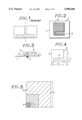
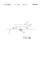
- FIG. 1 shows a top view of a known folded dipole of the prior art
- FIGS. 2, 3 and 4 each present a view in perspective, a side view and a top view respectively of a particular embodiment of the antenna according to the invention, called a short-circuited multilayer C type antenna;
- FIG. 3b presents a side view of an alternative embodiment of the invention.
- FIG. 5 enables the dimensions of the antennas according to the particular embodiment of the invention to be compared with those of conventional antennas
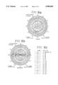
- FIGS. 6(a) and 6(b) each show a radiation pattern of an exemplary short-circuited multilayer C type antenna such as the one shown in FIGS. 2, 3 and 4, for main polarization (FIG. 6(a)) and crossed polarization (FIG. 6(b)) respectively;
- FIG. 6(c) shows a table of correspondence of the references of the contour lines of FIGS. 6(a) and 6(b).
- the invention therefore relates to a small-sized planar antenna comprising, in particular, two conductive elements or patches that are superimposed (so as to be parallel to the ground plane) and short-circuited with respect to each other.
- the lower patch and the ground plane may also be short-circuited.
- the two patches may have one or more slots.
- FIGS. 2, 3 and 4 each present a view in perspective, a side view and a top view respectively of this short-circuited multilayer C type antenna according to the invention.
- This antenna comprises a ground plane 1 and two superimposed patches 2, 3 (called the lower patch 2 and the upper patch 3). It also includes a coaxial supply 4.
- the lower patch 2 and the upper patch 3 are identical. Each has a "C" shape, a slot 5, 5' made in an initially square shape defining a first free end 6, 6' and a second free end 7, 7'.
- the first free ends 6, 6' of the two patches 2, 3 are connected by a short-circuit 8.
- FIG. 3b shows an alternative embodiment of the invention, similar to FIG. 3, but further including a second short circuit 10 which connects the lower patch 2 with the ground plane 1.
- FIG. 1 shows a top view of a folded dipole known in the prior art.
- the short-circuited multilayer C type antenna of the invention is obtained by "folding" this folded dipole about its axis of symmetry xx'. It is the two half antennas obtained, which are identical and superimposed, that constitute the lower patch 2 and upper patch 3.
- the metal strip that joins them constitutes the short circuit 8 between the two patches 2, 3.
- the short-circuited multilayer C type antenna appears to use the first mode (usually the non-radiating mode) of the folded dipole. If it is assumed that the current distribution of the first embodiment of the first dipole is maintained, then the two half antennas obtained, which are now superimposed, have similar patterns of current distribution and their values of radiation are added together. Thus, the radiation is created while, at the same time, the surface area of the antenna is reduced in a ratio of 2.
- the antenna is entirely metallic.
- the antenna has a thickness of 6 mm (h 1 +h 2 ), and a total space requirement of 20 ⁇ 20 ⁇ 6 mm.
- the antenna has a thickness of 3 mm (h 1 +h 2 ), and a total space requirement of 13.5 ⁇ 13.5 ⁇ 6 mm.
- a resonance at a frequency of 1.2 GHz is obtained.
- a standard square-shaped element at the same frequency would have dimensions six times greater.
- the passband obtained is 2.5% for an S.W.R. of less than 2.
- FIGS. 6(a) and 6(b) each show a radiation pattern of this first exemplary short-circuited multilayer C type antenna, for the main polarization (FIG. 6(a)) and the crossed polarization (FIG. 6(b)) respectively.
- FIG. 6(c) shows a table of correspondence of the references of the contour lines of FIGS. 6(a) and 6(b).
- the antenna of the second example (comprising substrate) has a resonance at a frequency of 1.47 GHz, with a passband of 0.3% at an S.W.R. equal to 2.
- FIG. 5 enables the dimensions of the antennas according to the different embodiments of the invention to be compared with those of the standard antennas.
- the square 91 with a side ⁇ /12, with ⁇ as the operating wavelength of the antenna corresponds to the dimensions of the superimposed and short-circuited patches of the multilayer C type antenna of the invention.
- this multilayer C type antenna is the smallest that has been made. Its small passband (2.5%) could be increased by the optimization of its geometry.
- the square 93 with a side ⁇ /2 recalls the dimensions of the single patch used in standard antennas.
- the position and shape of the slot(s) or of the partial short-circuit(s) can be determined by:
Landscapes
- Waveguide Aerials (AREA)
- Details Of Aerials (AREA)
Abstract
Description
              TABLE I
______________________________________
Type of h.sub.1
               h.sub.2        l.sub.1
                                   l.sub.2
                                        l.sub.3
                                             w.sub.1
                                                  w.sub.2
antenna (mm)   (mm)   ε.sub.r1
                          ε.sub.r2
                              (mm) (mm) (mm) (mm) (mm)
______________________________________
without 3      3      1   1   12   4    4    4    16
substrate
with    1.5    1.5    1   2.2  7   3.5  3    3.5  10
substrate
______________________________________
Claims (4)
Applications Claiming Priority (2)
| Application Number | Priority Date | Filing Date | Title |
|---|---|---|---|
| FR9610459 | 1996-08-21 | ||
| FR9610459A FR2752646B1 (en) | 1996-08-21 | 1996-08-21 | FLAT PRINTED ANTENNA WITH SHORT-LAYERED ELEMENTS |
Publications (1)
| Publication Number | Publication Date |
|---|---|
| US5986606A true US5986606A (en) | 1999-11-16 |
Family
ID=9495216
Family Applications (1)
| Application Number | Title | Priority Date | Filing Date |
|---|---|---|---|
| US08/911,776 Expired - Fee Related US5986606A (en) | 1996-08-21 | 1997-08-15 | Planar printed-circuit antenna with short-circuited superimposed elements |
Country Status (6)
| Country | Link |
|---|---|
| US (1) | US5986606A (en) |
| EP (1) | EP0825673B1 (en) |
| CN (1) | CN1174522C (en) |
| CA (1) | CA2213155A1 (en) |
| DE (1) | DE69740078D1 (en) |
| FR (1) | FR2752646B1 (en) |
Cited By (64)
| Publication number | Priority date | Publication date | Assignee | Title |
|---|---|---|---|---|
| US6195051B1 (en) * | 1999-04-08 | 2001-02-27 | Motorola, Inc. | Microstrip antenna and method of forming same |
| US6195048B1 (en) * | 1997-12-01 | 2001-02-27 | Kabushiki Kaisha Toshiba | Multifrequency inverted F-type antenna |
| US6218991B1 (en) | 1999-08-27 | 2001-04-17 | Mohamed Sanad | Compact planar inverted F antenna |
| US6268831B1 (en) * | 2000-04-04 | 2001-07-31 | Ericsson Inc. | Inverted-f antennas with multiple planar radiating elements and wireless communicators incorporating same |
| WO2001063690A3 (en) * | 2000-02-22 | 2002-01-31 | Ericsson Telefon Ab L M | Small-size broad-band printed antenna with parasitic element |
| US6421014B1 (en) | 1999-10-12 | 2002-07-16 | Mohamed Sanad | Compact dual narrow band microstrip antenna |
| US6429819B1 (en) | 2001-04-06 | 2002-08-06 | Tyco Electronics Logistics Ag | Dual band patch bowtie slot antenna structure |
| US6556812B1 (en) * | 1998-11-04 | 2003-04-29 | Nokia Mobile Phones Limited | Antenna coupler and arrangement for coupling a radio telecommunication device to external apparatuses |
| US6573867B1 (en) | 2002-02-15 | 2003-06-03 | Ethertronics, Inc. | Small embedded multi frequency antenna for portable wireless communications |
| US20030201942A1 (en) * | 2002-04-25 | 2003-10-30 | Ethertronics, Inc. | Low-profile, multi-frequency, multi-band, capacitively loaded magnetic dipole antenna |
| US20030222826A1 (en) * | 2002-05-31 | 2003-12-04 | Ethertronics, Inc. | Multi-band, low-profile, capacitively loaded antennas with integrated filters |
| US6680704B2 (en) * | 2001-05-03 | 2004-01-20 | Telefonaktiebolaget Lm Ericsson(Publ) | Built-in patch antenna |
| US20040032368A1 (en) * | 2002-08-19 | 2004-02-19 | Spittler Shelly D. | Compact stacked quarter-wave circularly polarized SDS patch antenna |
| US20040095281A1 (en) * | 2002-11-18 | 2004-05-20 | Gregory Poilasne | Multi-band reconfigurable capacitively loaded magnetic dipole |
| US20040125026A1 (en) * | 2002-12-17 | 2004-07-01 | Ethertronics, Inc. | Antennas with reduced space and improved performance |
| US20040145523A1 (en) * | 2003-01-27 | 2004-07-29 | Jeff Shamblin | Differential mode capacitively loaded magnetic dipole antenna |
| US20040155823A1 (en) * | 2001-06-12 | 2004-08-12 | Georges Kossiavas | Compact multiband antenna |
| US20040183730A1 (en) * | 2001-06-08 | 2004-09-23 | Bernard Jecko | Omnidirectional resonant antenna |
| US20050030239A1 (en) * | 2002-07-26 | 2005-02-10 | Amphenol Socapex | Antenna of small dimensions |
| US6859175B2 (en) | 2002-12-03 | 2005-02-22 | Ethertronics, Inc. | Multiple frequency antennas with reduced space and relative assembly |
| US20050110698A1 (en) * | 2003-11-24 | 2005-05-26 | Sandbridge Technologies Inc. | Modified printed dipole antennas for wireless multi-band communication systems |
| US20050110696A1 (en) * | 2003-11-24 | 2005-05-26 | Sandbridge Technologies Inc. | Modified printed dipole antennas for wireless multi-band communication systems |
| US20050248488A1 (en) * | 2004-05-05 | 2005-11-10 | Tdk Corporation | Planar antenna |
| US7012568B2 (en) | 2001-06-26 | 2006-03-14 | Ethertronics, Inc. | Multi frequency magnetic dipole antenna structures and methods of reusing the volume of an antenna |
| US7123209B1 (en) | 2003-02-26 | 2006-10-17 | Ethertronics, Inc. | Low-profile, multi-frequency, differential antenna structures |
| KR100688648B1 (en) | 2005-12-30 | 2007-03-02 | 아로 주식회사 | Multiband internal antenna for mobile communication terminal using short stub |
| US7203533B1 (en) * | 2001-08-15 | 2007-04-10 | Bellsouth Intellectual Property Corp. | Multipurpose antenna accessory for protection of portable wireless communication devices |
| EP2495809A1 (en) * | 2011-03-03 | 2012-09-05 | Nxp B.V. | Multiband antenna |
| CN102800928A (en) * | 2011-05-27 | 2012-11-28 | 三星电子株式会社 | Antenna structure and electronic device including the antenna structure |
| US8466756B2 (en) | 2007-04-19 | 2013-06-18 | Pulse Finland Oy | Methods and apparatus for matching an antenna |
| US8473017B2 (en) | 2005-10-14 | 2013-06-25 | Pulse Finland Oy | Adjustable antenna and methods |
| US8564485B2 (en) | 2005-07-25 | 2013-10-22 | Pulse Finland Oy | Adjustable multiband antenna and methods |
| US8618990B2 (en) | 2011-04-13 | 2013-12-31 | Pulse Finland Oy | Wideband antenna and methods |
| US8629813B2 (en) | 2007-08-30 | 2014-01-14 | Pusle Finland Oy | Adjustable multi-band antenna and methods |
| US8648752B2 (en) | 2011-02-11 | 2014-02-11 | Pulse Finland Oy | Chassis-excited antenna apparatus and methods |
| US8786499B2 (en) | 2005-10-03 | 2014-07-22 | Pulse Finland Oy | Multiband antenna system and methods |
| US8847833B2 (en) | 2009-12-29 | 2014-09-30 | Pulse Finland Oy | Loop resonator apparatus and methods for enhanced field control |
| US8866689B2 (en) | 2011-07-07 | 2014-10-21 | Pulse Finland Oy | Multi-band antenna and methods for long term evolution wireless system |
| US8988296B2 (en) | 2012-04-04 | 2015-03-24 | Pulse Finland Oy | Compact polarized antenna and methods |
| US9123990B2 (en) | 2011-10-07 | 2015-09-01 | Pulse Finland Oy | Multi-feed antenna apparatus and methods |
| US9203154B2 (en) | 2011-01-25 | 2015-12-01 | Pulse Finland Oy | Multi-resonance antenna, antenna module, radio device and methods |
| US9246210B2 (en) | 2010-02-18 | 2016-01-26 | Pulse Finland Oy | Antenna with cover radiator and methods |
| US9350081B2 (en) | 2014-01-14 | 2016-05-24 | Pulse Finland Oy | Switchable multi-radiator high band antenna apparatus |
| US9406998B2 (en) | 2010-04-21 | 2016-08-02 | Pulse Finland Oy | Distributed multiband antenna and methods |
| US9450291B2 (en) | 2011-07-25 | 2016-09-20 | Pulse Finland Oy | Multiband slot loop antenna apparatus and methods |
| US9461371B2 (en) | 2009-11-27 | 2016-10-04 | Pulse Finland Oy | MIMO antenna and methods |
| US9484619B2 (en) | 2011-12-21 | 2016-11-01 | Pulse Finland Oy | Switchable diversity antenna apparatus and methods |
| US9531058B2 (en) | 2011-12-20 | 2016-12-27 | Pulse Finland Oy | Loosely-coupled radio antenna apparatus and methods |
| US9590308B2 (en) | 2013-12-03 | 2017-03-07 | Pulse Electronics, Inc. | Reduced surface area antenna apparatus and mobile communications devices incorporating the same |
| US9634383B2 (en) | 2013-06-26 | 2017-04-25 | Pulse Finland Oy | Galvanically separated non-interacting antenna sector apparatus and methods |
| US9647338B2 (en) | 2013-03-11 | 2017-05-09 | Pulse Finland Oy | Coupled antenna structure and methods |
| US9673507B2 (en) | 2011-02-11 | 2017-06-06 | Pulse Finland Oy | Chassis-excited antenna apparatus and methods |
| US9680212B2 (en) | 2013-11-20 | 2017-06-13 | Pulse Finland Oy | Capacitive grounding methods and apparatus for mobile devices |
| US9722308B2 (en) | 2014-08-28 | 2017-08-01 | Pulse Finland Oy | Low passive intermodulation distributed antenna system for multiple-input multiple-output systems and methods of use |
| US9761951B2 (en) | 2009-11-03 | 2017-09-12 | Pulse Finland Oy | Adjustable antenna apparatus and methods |
| US9906260B2 (en) | 2015-07-30 | 2018-02-27 | Pulse Finland Oy | Sensor-based closed loop antenna swapping apparatus and methods |
| US9948002B2 (en) | 2014-08-26 | 2018-04-17 | Pulse Finland Oy | Antenna apparatus with an integrated proximity sensor and methods |
| US9973228B2 (en) | 2014-08-26 | 2018-05-15 | Pulse Finland Oy | Antenna apparatus with an integrated proximity sensor and methods |
| US9979078B2 (en) | 2012-10-25 | 2018-05-22 | Pulse Finland Oy | Modular cell antenna apparatus and methods |
| US10069209B2 (en) | 2012-11-06 | 2018-09-04 | Pulse Finland Oy | Capacitively coupled antenna apparatus and methods |
| US10079428B2 (en) | 2013-03-11 | 2018-09-18 | Pulse Finland Oy | Coupled antenna structure and methods |
| US20200168995A1 (en) * | 2018-11-27 | 2020-05-28 | Inventec (Pudong) Technology Corporation | Metal-inteference-resisting dipole antenna |
| US20250062531A1 (en) * | 2022-01-12 | 2025-02-20 | Sony Group Corporation | Antenna device, antenna module, and radio device |
| US12407112B2 (en) * | 2022-03-24 | 2025-09-02 | Honor Device Co., Ltd. | Antenna, ultra wide band antenna array, and electronic device |
Families Citing this family (4)
| Publication number | Priority date | Publication date | Assignee | Title |
|---|---|---|---|---|
| KR100483043B1 (en) * | 2002-04-11 | 2005-04-18 | 삼성전기주식회사 | Multi band built-in antenna |
| CN103098302B (en) * | 2010-09-15 | 2016-01-27 | 迪睿合电子材料有限公司 | Antenna assembly and communicator |
| WO2012129901A1 (en) * | 2011-04-01 | 2012-10-04 | 深圳光启高等理工研究院 | Antenna and mimo antenna having the antenna |
| CN102760941B (en) * | 2011-04-29 | 2015-11-18 | 深圳光启高等理工研究院 | A kind of radiofrequency antenna made of metamaterial with multi layer substrate and preparation method thereof |
Citations (7)
| Publication number | Priority date | Publication date | Assignee | Title |
|---|---|---|---|---|
| US4162499A (en) * | 1977-10-26 | 1979-07-24 | The United States Of America As Represented By The Secretary Of The Army | Flush-mounted piggyback microstrip antenna |
| JPS6058704A (en) * | 1983-09-09 | 1985-04-04 | Nippon Telegr & Teleph Corp <Ntt> | Double resonance type inverted-f antenna |
| FR2552938A1 (en) * | 1983-10-04 | 1985-04-05 | Dassault Electronique | RADIANT DEVICE WITH IMPROVED MICRO-TAPE STRUCTURE AND APPLICATION TO AN ADAPTIVE ANTENNA |
| JPS6141205A (en) * | 1984-08-01 | 1986-02-27 | Nippon Telegr & Teleph Corp <Ntt> | Antenna for wide-band transmission line |
| US5621571A (en) * | 1994-02-14 | 1997-04-15 | Minnesota Mining And Manufacturing Company | Integrated retroreflective electronic display |
| US5680144A (en) * | 1996-03-13 | 1997-10-21 | Nokia Mobile Phones Limited | Wideband, stacked double C-patch antenna having gap-coupled parasitic elements |
| US5703601A (en) * | 1996-09-09 | 1997-12-30 | The United States Of America As Represented By The Secretary Of The Army | Double layer circularly polarized antenna with single feed |
Family Cites Families (3)
| Publication number | Priority date | Publication date | Assignee | Title |
|---|---|---|---|---|
| US4131893A (en) * | 1977-04-01 | 1978-12-26 | Ball Corporation | Microstrip radiator with folded resonant cavity |
| FR2718292B1 (en) * | 1994-04-01 | 1996-06-28 | Christian Sabatier | Antenna for transmitting and / or receiving electromagnetic signals, in particular microwave frequencies, and device using such an antenna. |
| DE59708915D1 (en) * | 1996-03-13 | 2003-01-23 | Ascom Systec Ag Maegenwil | Flat three-dimensional antenna |
-
1996
- 1996-08-21 FR FR9610459A patent/FR2752646B1/en not_active Expired - Lifetime
-
1997
- 1997-08-14 DE DE69740078T patent/DE69740078D1/en not_active Expired - Lifetime
- 1997-08-14 EP EP97460030A patent/EP0825673B1/en not_active Expired - Lifetime
- 1997-08-15 US US08/911,776 patent/US5986606A/en not_active Expired - Fee Related
- 1997-08-18 CA CA002213155A patent/CA2213155A1/en not_active Abandoned
- 1997-08-21 CN CNB971192952A patent/CN1174522C/en not_active Expired - Lifetime
Patent Citations (7)
| Publication number | Priority date | Publication date | Assignee | Title |
|---|---|---|---|---|
| US4162499A (en) * | 1977-10-26 | 1979-07-24 | The United States Of America As Represented By The Secretary Of The Army | Flush-mounted piggyback microstrip antenna |
| JPS6058704A (en) * | 1983-09-09 | 1985-04-04 | Nippon Telegr & Teleph Corp <Ntt> | Double resonance type inverted-f antenna |
| FR2552938A1 (en) * | 1983-10-04 | 1985-04-05 | Dassault Electronique | RADIANT DEVICE WITH IMPROVED MICRO-TAPE STRUCTURE AND APPLICATION TO AN ADAPTIVE ANTENNA |
| JPS6141205A (en) * | 1984-08-01 | 1986-02-27 | Nippon Telegr & Teleph Corp <Ntt> | Antenna for wide-band transmission line |
| US5621571A (en) * | 1994-02-14 | 1997-04-15 | Minnesota Mining And Manufacturing Company | Integrated retroreflective electronic display |
| US5680144A (en) * | 1996-03-13 | 1997-10-21 | Nokia Mobile Phones Limited | Wideband, stacked double C-patch antenna having gap-coupled parasitic elements |
| US5703601A (en) * | 1996-09-09 | 1997-12-30 | The United States Of America As Represented By The Secretary Of The Army | Double layer circularly polarized antenna with single feed |
Cited By (84)
| Publication number | Priority date | Publication date | Assignee | Title |
|---|---|---|---|---|
| US6195048B1 (en) * | 1997-12-01 | 2001-02-27 | Kabushiki Kaisha Toshiba | Multifrequency inverted F-type antenna |
| US6556812B1 (en) * | 1998-11-04 | 2003-04-29 | Nokia Mobile Phones Limited | Antenna coupler and arrangement for coupling a radio telecommunication device to external apparatuses |
| US6195051B1 (en) * | 1999-04-08 | 2001-02-27 | Motorola, Inc. | Microstrip antenna and method of forming same |
| US6218991B1 (en) | 1999-08-27 | 2001-04-17 | Mohamed Sanad | Compact planar inverted F antenna |
| US6421014B1 (en) | 1999-10-12 | 2002-07-16 | Mohamed Sanad | Compact dual narrow band microstrip antenna |
| WO2001063690A3 (en) * | 2000-02-22 | 2002-01-31 | Ericsson Telefon Ab L M | Small-size broad-band printed antenna with parasitic element |
| US6268831B1 (en) * | 2000-04-04 | 2001-07-31 | Ericsson Inc. | Inverted-f antennas with multiple planar radiating elements and wireless communicators incorporating same |
| US6429819B1 (en) | 2001-04-06 | 2002-08-06 | Tyco Electronics Logistics Ag | Dual band patch bowtie slot antenna structure |
| US6680704B2 (en) * | 2001-05-03 | 2004-01-20 | Telefonaktiebolaget Lm Ericsson(Publ) | Built-in patch antenna |
| US20040183730A1 (en) * | 2001-06-08 | 2004-09-23 | Bernard Jecko | Omnidirectional resonant antenna |
| US7170448B2 (en) * | 2001-06-08 | 2007-01-30 | Centre National De La Recherche Scientifique (C.N.R.S.) | Omnidirectional resonant antenna |
| JP2004529592A (en) * | 2001-06-12 | 2004-09-24 | アルカテル | Small multi-band antenna |
| US20040155823A1 (en) * | 2001-06-12 | 2004-08-12 | Georges Kossiavas | Compact multiband antenna |
| US6930642B2 (en) * | 2001-06-12 | 2005-08-16 | Alcatel | Compact multiband antenna |
| US7012568B2 (en) | 2001-06-26 | 2006-03-14 | Ethertronics, Inc. | Multi frequency magnetic dipole antenna structures and methods of reusing the volume of an antenna |
| US7203533B1 (en) * | 2001-08-15 | 2007-04-10 | Bellsouth Intellectual Property Corp. | Multipurpose antenna accessory for protection of portable wireless communication devices |
| US6573867B1 (en) | 2002-02-15 | 2003-06-03 | Ethertronics, Inc. | Small embedded multi frequency antenna for portable wireless communications |
| US20030201942A1 (en) * | 2002-04-25 | 2003-10-30 | Ethertronics, Inc. | Low-profile, multi-frequency, multi-band, capacitively loaded magnetic dipole antenna |
| US6943730B2 (en) | 2002-04-25 | 2005-09-13 | Ethertronics Inc. | Low-profile, multi-frequency, multi-band, capacitively loaded magnetic dipole antenna |
| US20030222826A1 (en) * | 2002-05-31 | 2003-12-04 | Ethertronics, Inc. | Multi-band, low-profile, capacitively loaded antennas with integrated filters |
| US20050030239A1 (en) * | 2002-07-26 | 2005-02-10 | Amphenol Socapex | Antenna of small dimensions |
| US20040032368A1 (en) * | 2002-08-19 | 2004-02-19 | Spittler Shelly D. | Compact stacked quarter-wave circularly polarized SDS patch antenna |
| US6995709B2 (en) * | 2002-08-19 | 2006-02-07 | Raytheon Company | Compact stacked quarter-wave circularly polarized SDS patch antenna |
| US20040095281A1 (en) * | 2002-11-18 | 2004-05-20 | Gregory Poilasne | Multi-band reconfigurable capacitively loaded magnetic dipole |
| US6911940B2 (en) | 2002-11-18 | 2005-06-28 | Ethertronics, Inc. | Multi-band reconfigurable capacitively loaded magnetic dipole |
| US6859175B2 (en) | 2002-12-03 | 2005-02-22 | Ethertronics, Inc. | Multiple frequency antennas with reduced space and relative assembly |
| US7084813B2 (en) | 2002-12-17 | 2006-08-01 | Ethertronics, Inc. | Antennas with reduced space and improved performance |
| US20040125026A1 (en) * | 2002-12-17 | 2004-07-01 | Ethertronics, Inc. | Antennas with reduced space and improved performance |
| US20040145523A1 (en) * | 2003-01-27 | 2004-07-29 | Jeff Shamblin | Differential mode capacitively loaded magnetic dipole antenna |
| US6919857B2 (en) | 2003-01-27 | 2005-07-19 | Ethertronics, Inc. | Differential mode capacitively loaded magnetic dipole antenna |
| US7123209B1 (en) | 2003-02-26 | 2006-10-17 | Ethertronics, Inc. | Low-profile, multi-frequency, differential antenna structures |
| US7034769B2 (en) | 2003-11-24 | 2006-04-25 | Sandbridge Technologies, Inc. | Modified printed dipole antennas for wireless multi-band communication systems |
| US7095382B2 (en) | 2003-11-24 | 2006-08-22 | Sandbridge Technologies, Inc. | Modified printed dipole antennas for wireless multi-band communications systems |
| US20060208956A1 (en) * | 2003-11-24 | 2006-09-21 | Emanoil Surducan | Modified printed dipole antennas for wireless multi-band communication systems |
| US20050110698A1 (en) * | 2003-11-24 | 2005-05-26 | Sandbridge Technologies Inc. | Modified printed dipole antennas for wireless multi-band communication systems |
| US20050110696A1 (en) * | 2003-11-24 | 2005-05-26 | Sandbridge Technologies Inc. | Modified printed dipole antennas for wireless multi-band communication systems |
| US7042402B2 (en) * | 2004-05-05 | 2006-05-09 | Tdk Corporation | Planar antenna |
| US20050248488A1 (en) * | 2004-05-05 | 2005-11-10 | Tdk Corporation | Planar antenna |
| US8564485B2 (en) | 2005-07-25 | 2013-10-22 | Pulse Finland Oy | Adjustable multiband antenna and methods |
| US8786499B2 (en) | 2005-10-03 | 2014-07-22 | Pulse Finland Oy | Multiband antenna system and methods |
| US8473017B2 (en) | 2005-10-14 | 2013-06-25 | Pulse Finland Oy | Adjustable antenna and methods |
| KR100688648B1 (en) | 2005-12-30 | 2007-03-02 | 아로 주식회사 | Multiband internal antenna for mobile communication terminal using short stub |
| US8466756B2 (en) | 2007-04-19 | 2013-06-18 | Pulse Finland Oy | Methods and apparatus for matching an antenna |
| US8629813B2 (en) | 2007-08-30 | 2014-01-14 | Pusle Finland Oy | Adjustable multi-band antenna and methods |
| US9761951B2 (en) | 2009-11-03 | 2017-09-12 | Pulse Finland Oy | Adjustable antenna apparatus and methods |
| US9461371B2 (en) | 2009-11-27 | 2016-10-04 | Pulse Finland Oy | MIMO antenna and methods |
| US8847833B2 (en) | 2009-12-29 | 2014-09-30 | Pulse Finland Oy | Loop resonator apparatus and methods for enhanced field control |
| US9246210B2 (en) | 2010-02-18 | 2016-01-26 | Pulse Finland Oy | Antenna with cover radiator and methods |
| US9406998B2 (en) | 2010-04-21 | 2016-08-02 | Pulse Finland Oy | Distributed multiband antenna and methods |
| US9203154B2 (en) | 2011-01-25 | 2015-12-01 | Pulse Finland Oy | Multi-resonance antenna, antenna module, radio device and methods |
| US9673507B2 (en) | 2011-02-11 | 2017-06-06 | Pulse Finland Oy | Chassis-excited antenna apparatus and methods |
| US8648752B2 (en) | 2011-02-11 | 2014-02-11 | Pulse Finland Oy | Chassis-excited antenna apparatus and methods |
| US9917346B2 (en) | 2011-02-11 | 2018-03-13 | Pulse Finland Oy | Chassis-excited antenna apparatus and methods |
| EP2495809A1 (en) * | 2011-03-03 | 2012-09-05 | Nxp B.V. | Multiband antenna |
| US9190719B2 (en) | 2011-03-03 | 2015-11-17 | Nxp B.V. | Multiband antenna |
| US8618990B2 (en) | 2011-04-13 | 2013-12-31 | Pulse Finland Oy | Wideband antenna and methods |
| US9123994B2 (en) * | 2011-05-27 | 2015-09-01 | Samsung Electronics Co., Ltd. | Antenna structure |
| AU2012263216B2 (en) * | 2011-05-27 | 2016-04-28 | Samsung Electronics Co., Ltd. | Antenna structure |
| CN102800928B (en) * | 2011-05-27 | 2017-05-03 | 三星电子株式会社 | Antenna structure and electronic device comprising the same |
| US20120299783A1 (en) * | 2011-05-27 | 2012-11-29 | Samsung Electronics Co., Ltd. | Antenna structure |
| CN102800928A (en) * | 2011-05-27 | 2012-11-28 | 三星电子株式会社 | Antenna structure and electronic device including the antenna structure |
| US8866689B2 (en) | 2011-07-07 | 2014-10-21 | Pulse Finland Oy | Multi-band antenna and methods for long term evolution wireless system |
| US9450291B2 (en) | 2011-07-25 | 2016-09-20 | Pulse Finland Oy | Multiband slot loop antenna apparatus and methods |
| US9123990B2 (en) | 2011-10-07 | 2015-09-01 | Pulse Finland Oy | Multi-feed antenna apparatus and methods |
| US9531058B2 (en) | 2011-12-20 | 2016-12-27 | Pulse Finland Oy | Loosely-coupled radio antenna apparatus and methods |
| US9484619B2 (en) | 2011-12-21 | 2016-11-01 | Pulse Finland Oy | Switchable diversity antenna apparatus and methods |
| US9509054B2 (en) | 2012-04-04 | 2016-11-29 | Pulse Finland Oy | Compact polarized antenna and methods |
| US8988296B2 (en) | 2012-04-04 | 2015-03-24 | Pulse Finland Oy | Compact polarized antenna and methods |
| US9979078B2 (en) | 2012-10-25 | 2018-05-22 | Pulse Finland Oy | Modular cell antenna apparatus and methods |
| US10069209B2 (en) | 2012-11-06 | 2018-09-04 | Pulse Finland Oy | Capacitively coupled antenna apparatus and methods |
| US9647338B2 (en) | 2013-03-11 | 2017-05-09 | Pulse Finland Oy | Coupled antenna structure and methods |
| US10079428B2 (en) | 2013-03-11 | 2018-09-18 | Pulse Finland Oy | Coupled antenna structure and methods |
| US9634383B2 (en) | 2013-06-26 | 2017-04-25 | Pulse Finland Oy | Galvanically separated non-interacting antenna sector apparatus and methods |
| US9680212B2 (en) | 2013-11-20 | 2017-06-13 | Pulse Finland Oy | Capacitive grounding methods and apparatus for mobile devices |
| US9590308B2 (en) | 2013-12-03 | 2017-03-07 | Pulse Electronics, Inc. | Reduced surface area antenna apparatus and mobile communications devices incorporating the same |
| US9350081B2 (en) | 2014-01-14 | 2016-05-24 | Pulse Finland Oy | Switchable multi-radiator high band antenna apparatus |
| US9948002B2 (en) | 2014-08-26 | 2018-04-17 | Pulse Finland Oy | Antenna apparatus with an integrated proximity sensor and methods |
| US9973228B2 (en) | 2014-08-26 | 2018-05-15 | Pulse Finland Oy | Antenna apparatus with an integrated proximity sensor and methods |
| US9722308B2 (en) | 2014-08-28 | 2017-08-01 | Pulse Finland Oy | Low passive intermodulation distributed antenna system for multiple-input multiple-output systems and methods of use |
| US9906260B2 (en) | 2015-07-30 | 2018-02-27 | Pulse Finland Oy | Sensor-based closed loop antenna swapping apparatus and methods |
| US20200168995A1 (en) * | 2018-11-27 | 2020-05-28 | Inventec (Pudong) Technology Corporation | Metal-inteference-resisting dipole antenna |
| US10784580B2 (en) * | 2018-11-27 | 2020-09-22 | Inventec (Pudong) Technology Corporation | Metal-inteference-resisting dipole antenna |
| US20250062531A1 (en) * | 2022-01-12 | 2025-02-20 | Sony Group Corporation | Antenna device, antenna module, and radio device |
| US12407112B2 (en) * | 2022-03-24 | 2025-09-02 | Honor Device Co., Ltd. | Antenna, ultra wide band antenna array, and electronic device |
Also Published As
| Publication number | Publication date |
|---|---|
| EP0825673B1 (en) | 2010-12-15 |
| FR2752646A1 (en) | 1998-02-27 |
| CA2213155A1 (en) | 1998-02-21 |
| CN1174522C (en) | 2004-11-03 |
| FR2752646B1 (en) | 1998-11-13 |
| DE69740078D1 (en) | 2011-01-27 |
| EP0825673A1 (en) | 1998-02-25 |
| CN1180947A (en) | 1998-05-06 |
Similar Documents
| Publication | Publication Date | Title |
|---|---|---|
| US5986606A (en) | Planar printed-circuit antenna with short-circuited superimposed elements | |
| US11575206B2 (en) | Self-filtering wideband millimeter wave antenna | |
| US5410323A (en) | Planar antenna | |
| US5568155A (en) | Antenna devices having double-resonance characteristics | |
| US6741210B2 (en) | Dual band printed antenna | |
| US4083046A (en) | Electric monomicrostrip dipole antennas | |
| Mao et al. | Multimode resonator-fed dual-polarized antenna array with enhanced bandwidth and selectivity | |
| US6337667B1 (en) | Multiband, single feed antenna | |
| EP1590857B1 (en) | Low profile dual frequency dipole antenna structure | |
| US4613868A (en) | Method and apparatus for matched impedance feeding of microstrip-type radio frequency antenna structure | |
| US5914695A (en) | Omnidirectional dipole antenna | |
| EP1251588A2 (en) | Method for tuning an antenna and an antenna | |
| US7642981B2 (en) | Wide-band slot antenna apparatus with constant beam width | |
| DE60123963T2 (en) | ANTENNA AND RADIO COMMUNICATION DEVICE WITH SUCH ANTENNA | |
| KR100449396B1 (en) | Patch antenna and electronic equipment using the same | |
| US20220224017A1 (en) | Capacitive-coupled comb-line microstrip array antenna and method of manufacturing the same | |
| US4167010A (en) | Terminated microstrip antenna | |
| EP4075601B1 (en) | Antenna structure and wireless communication device | |
| Ghaloua et al. | Mutual coupling reduction and miniaturization arrays antennas using new structure of EBG | |
| DE60122698T2 (en) | Multi-band antenna | |
| EP0519508B1 (en) | Printed antenna | |
| US4660047A (en) | Microstrip antenna with resonator feed | |
| CN111628287A (en) | Broadband circularly polarized patch antenna | |
| Carrasquillo-Rivera et al. | Tunable and dual-band rectangular slot-ring antenna | |
| Naresh Kumar | Asymmetric CPW fed miniaturized dual polarized monopole antenna for WLAN/WiMAX applications |
Legal Events
| Date | Code | Title | Description |
|---|---|---|---|
| AS | Assignment |
Owner name: FRANCE TELECOM, FRANCE Free format text: ASSIGNMENT OF ASSIGNORS INTEREST;ASSIGNORS:KOSSIAVAS, GEORGES;PAPIERNIK, ALBERT;BRACHAT, PATRICE;AND OTHERS;REEL/FRAME:009286/0713 Effective date: 19970815 |
|
| FEPP | Fee payment procedure |
Free format text: PAYOR NUMBER ASSIGNED (ORIGINAL EVENT CODE: ASPN); ENTITY STATUS OF PATENT OWNER: LARGE ENTITY |
|
| FEPP | Fee payment procedure |
Free format text: PAYER NUMBER DE-ASSIGNED (ORIGINAL EVENT CODE: RMPN); ENTITY STATUS OF PATENT OWNER: LARGE ENTITY |
|
| FPAY | Fee payment |
Year of fee payment: 4 |
|
| REMI | Maintenance fee reminder mailed | ||
| FEPP | Fee payment procedure |
Free format text: PAYER NUMBER DE-ASSIGNED (ORIGINAL EVENT CODE: RMPN); ENTITY STATUS OF PATENT OWNER: LARGE ENTITY Free format text: PAYOR NUMBER ASSIGNED (ORIGINAL EVENT CODE: ASPN); ENTITY STATUS OF PATENT OWNER: LARGE ENTITY |
|
| FPAY | Fee payment |
Year of fee payment: 8 |
|
| FEPP | Fee payment procedure |
Free format text: PAYER NUMBER DE-ASSIGNED (ORIGINAL EVENT CODE: RMPN); ENTITY STATUS OF PATENT OWNER: LARGE ENTITY Free format text: PAYOR NUMBER ASSIGNED (ORIGINAL EVENT CODE: ASPN); ENTITY STATUS OF PATENT OWNER: LARGE ENTITY |
|
| AS | Assignment |
Owner name: GULA CONSULTING LIMITED LIABILITY COMPANY, DELAWAR Free format text: ASSIGNMENT OF ASSIGNORS INTEREST;ASSIGNOR:FRANCE TELECOM SA;REEL/FRAME:022354/0124 Effective date: 20081202 |
|
| REMI | Maintenance fee reminder mailed | ||
| LAPS | Lapse for failure to pay maintenance fees | ||
| STCH | Information on status: patent discontinuation |
Free format text: PATENT EXPIRED DUE TO NONPAYMENT OF MAINTENANCE FEES UNDER 37 CFR 1.362 |
|
| FP | Lapsed due to failure to pay maintenance fee |
Effective date: 20111116 |
|
| AS | Assignment |
Owner name: HANGER SOLUTIONS, LLC, GEORGIA Free format text: ASSIGNMENT OF ASSIGNORS INTEREST;ASSIGNOR:INTELLECTUAL VENTURES ASSETS 158 LLC;REEL/FRAME:051486/0425 Effective date: 20191206 |
|
| AS | Assignment |
Owner name: INTELLECTUAL VENTURES ASSETS 158 LLC, DELAWARE Free format text: ASSIGNMENT OF ASSIGNORS INTEREST;ASSIGNOR:GULA CONSULTING LIMITED LIABILITY COMPANY;REEL/FRAME:052159/0463 Effective date: 20191126 |