US5973934A - Printed circuit board latching mechanism - Google Patents
Printed circuit board latching mechanism Download PDFInfo
- Publication number
- US5973934A US5973934A US09/099,592 US9959298A US5973934A US 5973934 A US5973934 A US 5973934A US 9959298 A US9959298 A US 9959298A US 5973934 A US5973934 A US 5973934A
- Authority
- US
- United States
- Prior art keywords
- printed circuit
- circuit board
- set forth
- engageable
- cage
- Prior art date
- Legal status (The legal status is an assumption and is not a legal conclusion. Google has not performed a legal analysis and makes no representation as to the accuracy of the status listed.)
- Expired - Lifetime
Links
Images


Classifications
-
- H—ELECTRICITY
- H05—ELECTRIC TECHNIQUES NOT OTHERWISE PROVIDED FOR
- H05K—PRINTED CIRCUITS; CASINGS OR CONSTRUCTIONAL DETAILS OF ELECTRIC APPARATUS; MANUFACTURE OF ASSEMBLAGES OF ELECTRICAL COMPONENTS
- H05K7/00—Constructional details common to different types of electric apparatus
- H05K7/14—Mounting supporting structure in casing or on frame or rack
- H05K7/1401—Mounting supporting structure in casing or on frame or rack comprising clamping or extracting means
- H05K7/1402—Mounting supporting structure in casing or on frame or rack comprising clamping or extracting means for securing or extracting printed circuit boards
- H05K7/1409—Mounting supporting structure in casing or on frame or rack comprising clamping or extracting means for securing or extracting printed circuit boards by lever-type mechanisms
Definitions
- This invention relates generally to a mechanism for mounting a printed circuit board, and, more particularly, to a mechanism for latching a printed circuit board into an electrical connector.
- the individual metallic tabs are necessarily reduced in width to accommodate more metallic tabs.
- state-of-the-art microprocessor printed circuit boards have over 300 metallic tabs that measure 50 thousandths of an inch wide.
- the tabs are arranged in a tiered configuration with three tabs every 100 thousandths of an inch.
- These densely packed contacts can become misaligned with their corresponding edge connector by a relatively minor displacement of only 20 thousandths of an inch. That is, the printed circuit board can become uncoupled or disconnected from its corresponding electrical connector relatively easily. Disconnection, of course, prevents the electrical signals from being properly delivered to other printed circuit boards in the electrical system, which prevents proper operation of the system. Moreover, this relatively minor displacement is difficult to visually detect, and, thus, faulty operation is difficult to diagnose.
- the present invention is directed to overcoming, or at least reducing the effects of, one or more of the problems set forth above.
- an apparatus for coupling a printed circuit board within a printed circuit board cage.
- the apparatus includes a first portion coupled to the printed circuit board cage.
- the first portion has a bore formed therein.
- a second portion is rotatably coupled to the printed circuit board, and includes a cam surface formed on a first end portion thereof. The cam surface is engageable with an interior surface of the bore of the first portion to urge the second portion and the printed circuit board from a first position to a second position.
- the second portion also includes a latch formed on a second end portion thereof. The latch is engageable with a corresponding latch on the printed circuit board in response to the second portion being located in the second position.
- FIG. 1 illustrates a perspective of a personal computer, such as a server
- FIG. 2 illustrates a perspective view of a portion of a microprocessor cage and latching mechanism within the server of FIG. 1;
- FIG. 3 illustrates an exploded perspective view of a portion of the microprocessor cage and latching mechanism within the server of FIG. 1;
- FIGS. 4A and 4B respectively illustrate top views of a printed circuit board released and held in place by the latching mechanism of FIG. 3;
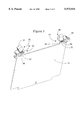
- FIG. 5 illustrates a perspective view of the latching mechanism of FIG. 3.
- FIG. 1 a perspective view of a personal computer, such as a server 10 is shown.
- the server 10 has a side access panel (not shown) removed, exposing a microprocessor cage 12 mounted to a motherboard (not shown).
- the microprocessor cage 12 houses a plurality of printed circuit boards 16.
- the printed circuit boards 16 are of two general types, a microprocessor printed circuit board assembly 18 and a voltage regulator module 20.
- the microprocessor printed circuit board assembly 18 contains a microprocessor (not shown), such as an Intel Pentium II, its associated circuitry (not shown), and a heat pipe 24.
- the voltage regulator module 20 is positioned adjacent the microprocessor printed circuit board assembly 18, generally providing the function of controlling voltages delivered to the microprocessor board assembly 18.
- four microprocessor printed circuit board assemblies 18 and four voltage regulator modules 20 are included within the microprocessor cage 12.
- the illustrated embodiment includes four microprocessor printed circuit board assemblies 18 and four voltage regulator modules 20, the invention is applicable to any number of microprocessor printed circuit board assemblies 18 and voltage regulator modules 20.
- the microprocessor cage 12 is mounted to the motherboard (not shown), which is vertically mounted within the server 10.
- the cage 12, the microprocessor printed circuit board assemblies 18, and the voltage regulator modules 20 are relatively heavy, and, accordingly, are mounted to a support member (not shown) connected to a frame (not shown) of the server 10, rather than only to the motherboard (not shown).
- latching mechanisms 26 are included for both locating the printed circuit boards 16 within their matching electrical connector (not shown), and helping to maintain the printed circuit boards 16 securely seated within their electrical connectors (not shown) during normal operation and shipping.
- a first type of latching mechanism 28 is associated with the voltage regulator modules 20, and a second type of latching mechanism 30 is associated with the microprocessor printed circuit board assemblies 18.
- the latching mechanism 28 associated with the voltage regulator modules 20 are discussed in more detail throughout this specification.
- the second type of latching mechanism 30 associated with the microprocessor printed circuit board assembly 18 is discussed in detail in co-pending application Ser. No. 09/009,585 filed contemporaneously with the current application, and subject to assignment to a common assignee.
- FIG. 2 a perspective view of the microprocessor cage 12 with the latching mechanism 28 of the voltage regulator module 20 installed therein is shown.
- the latching mechanism 28 includes a first pivoting portion 32 rotatably attached to the voltage regulator module 20, and a second fixed portion 34 coupled to the microprocessor cage 12.
- the rotating portion 32 is pivotable to a first position (as shown in FIG. 2) in which it engages the fixed portion 34 to removably couple the voltage regulator module 20 into its connector (not shown) and into the microprocessor cage 12.
- the rotating portion 32 is also used to assist in removing the voltage regulator module 20 from its connector (not shown) and the microprocessor cage 12. Pivoting the rotating portion 32 causes it to engage the fixed portion 34 and apply an outward force, urging the voltage regulator module 20 to decouple from its connector (not shown) and slide out from microprocessor cage 12 along a track (not shown) formed in the side of the microprocessor cage 12.
- FIG. 3 illustrates the voltage regulator module 20 being removed from the microprocessor cage 12, and the rotating portions 32 pivoted to their decoupling position.
- FIG. 4A a partial cross sectional top view of the voltage regulator module 20 and microprocessor cage 12 is shown.
- the voltage regulator module 20 is shown with the metallic tabs 40 of its edge connector 42 spaced from a connector 44, in position to be inserted into or removed from the connector 42.
- the fixed portion 34 is coupled to the microprocessor cage 12 by a pair of pawls 50, 52 extending through openings 54, 56 in the side of the microprocessor cage 12.
- a cantilever 58 locks the fixed portion 34 against removal from the microprocessor cage 12. That is, during assembly, the fixed portion 34 is positioned on the side of the microprocessor cage 12 with its pawls 50, 52 extending through the openings 54, 56.
- the fixed portion 34 is then moved longitudinally in a direction indicated by an arrow 57 to engage enlarged portions 51 of the pawls 50, 52 with the back and edge of the openings 54, 56.
- the cantilever 58 which by its construction is spring loaded in a direction toward the microprocessor cage 12, slides into an opening 60. With the cantilever 58 positioned in the opening 60, reverse longitudinal movement of the fixed portion 34 is prevented.
- a frustoconically shaped alignment pin 46 located on the back of the fixed portion 34 extends through a similarly sized opening 48 in the microprocessor cage 12 when the fixed portion 34 is moved to its final longitudinal position.
- the alignment pin 46 assists in locating the fixed portion 34 at its proper location to engage the rotating portion 32 of the latching mechanism 28.
- the fixed portion 34 has a bore 70 formed in an end portion 72 thereof.
- the bore 70 opens onto the end portion 72, removably receiving the rotating portion 32 therein.
- the bore 70 may be defined in a portion of the cage, obviating the need for a separate fixed portion 34.
- the rotating portion 32 has an opening 74 therein, through which the rotating portion 32 is coupled to the voltage regulator module 20 by, for example, a pin 76.
- the pin 76 can take on any of a variety of well-known configurations, such a screw, rivet, brad, split pin, or the like.
- a first end portion 78 of the rotating portion 34 has a first cam surface 80 formed thereon.
- a second end portion 82 of the rotating portion 34 is manually engageable to assist in inserting the voltage regulator module 20.
- the first end portion 78 is received in the bore 70 of the fixed portion 34 with the cam surface 80 engaging the interior wall of the bore 70. Urging the second end portion 82 in a direction indicated by an arrow 84 forces the cam surface 80 against the interior surface of the bore 70, moving the voltage regulator module 20 in the direction indicated by the arrow 57 and engaging the edge connector 42 with the connector 44.
- the latch 90 includes an opening 92 formed in the voltage regulator module 20 and an inclined and spring loaded surface 94 on the second end portion 82 of the rotating portion 32, as is more clearly illustrated in FIG. 5.
- the inclined surface 94 engages the voltage regulator module 20, causing the inclined surface 94 to be compressed until it aligns with the opening 92.
- the inclined surface 94 aligns with the opening 92, the inclined surface decompresses, extending into the opening 92.
- an end surface 96 engages a sidewall of the opening 92, preventing reverse movement of the voltage regulator module 20 unless the inclined surface 94 is manually compressed.
- compression of the inclined surface 94 is accomplished in the illustrated embodiment by deforming a U-shaped cross section 95 of the second end portion 82.
- the inclined surface 94 is attached to one leg of the U-shaped cross section 95 such that when the legs of the U-shaped section 95 are urged toward one another, the inclined surface 94 is withdrawn from the opening 92.
- the voltage regulator module 20 may also be inserted into the connector 44 by manually pushing on an end portion 86 of the voltage regulator module 20 in the direction indicated by the arrow 57.
- the rotating portion 32 is positioned with the first end portion 78 directed toward the connector 44, overlying at least a portion of the voltage regulator module 20.
- the first end portion 78 is split in two substantially similar halves that overly a portion of the front and back surfaces of the voltage regulator module 20. That is, the voltage regulator module 20 fits between the halves of the first end portion 78 when the first portion 32 is positioned in the insertion orientation.
- the rotating portion 32 has a tab 99 formed on the first end portion 78.
- the tab 99 engages a top surface 101 of the fixed portion 34 during installation of the voltage regulator module 20.
- the tab 99 is rotated about the pin 76 by contact with the top surface 101 of the fixed portion 34.
- Rotation of the rotating portion 32 causes its first end portion 78 to be inserted into the bore 70 of the fixed portion 34.
- the first end portion 78 of the rotating portion 32 has a second cam surface 100 that may engage an opposite interior surface of the bore 70, as compared to the interior surface engaged by the first cam surface 80. With the second cam surface 100 engaging the bore 70 of the fixed portion 34, the second end portion 82 of the rotating portion 32 is forced to move in the direction indicated by the arrow 84 until the edge connector 42 is seated in the connector 44 and the latch 90 is engaged.
- the second cam surface 100 also serves a second function. That is, the second cam surface 100 is used to disengage the edge connector 42 from the connector 44. The inclined surface 94 is compressed to remove it from the opening 92. Next, the second end portion 82 is rotated in a direction opposite to that indicated by the arrow 84, engaging the second cam surface 100 with the bore 70 of the fixed portion 34. A force exerted by the cam surface 100 on the bore 70 urges the voltage regulator module 20 in a direction opposite to that indicated by the arrow 57, removing the edge connector 42 from the connector 44. The tab 99 also contacts the top surface 101 of the fixed portion 32 to provide additional removing force.
- the relative positions of the fixed and rotating portions 34, 32 may be reversed without departing from the spirit and scope of the instant invention. That is, the fixed portion 34, with appropriate modifications, may be coupled to the voltage regulator module 20, and the rotating portion 32, with appropriate modifications, may be coupled to the microprocessor cage 12.
Landscapes
- Engineering & Computer Science (AREA)
- Microelectronics & Electronic Packaging (AREA)
- Coupling Device And Connection With Printed Circuit (AREA)
Abstract
Description
Claims (26)
Priority Applications (1)
| Application Number | Priority Date | Filing Date | Title |
|---|---|---|---|
| US09/099,592 US5973934A (en) | 1998-06-18 | 1998-06-18 | Printed circuit board latching mechanism |
Applications Claiming Priority (1)
| Application Number | Priority Date | Filing Date | Title |
|---|---|---|---|
| US09/099,592 US5973934A (en) | 1998-06-18 | 1998-06-18 | Printed circuit board latching mechanism |
Publications (1)
| Publication Number | Publication Date |
|---|---|
| US5973934A true US5973934A (en) | 1999-10-26 |
Family
ID=22275749
Family Applications (1)
| Application Number | Title | Priority Date | Filing Date |
|---|---|---|---|
| US09/099,592 Expired - Lifetime US5973934A (en) | 1998-06-18 | 1998-06-18 | Printed circuit board latching mechanism |
Country Status (1)
| Country | Link |
|---|---|
| US (1) | US5973934A (en) |
Cited By (6)
| Publication number | Priority date | Publication date | Assignee | Title |
|---|---|---|---|---|
| US6046913A (en) * | 1998-04-24 | 2000-04-04 | Lucent Technologies Inc. | Panel mounted power module with adaptor mounting bracket |
| US6293636B1 (en) | 1999-12-30 | 2001-09-25 | Gateway, Inc. | Device retention assembly |
| US6456489B1 (en) | 2000-05-25 | 2002-09-24 | Gateway, Inc. | Device retention apparatus |
| US6885550B1 (en) | 1999-08-26 | 2005-04-26 | Axxion Group Corporation | Screw less clip mounted computer drive |
| US20070058354A1 (en) * | 2005-09-13 | 2007-03-15 | International Business Machines Corporation | System and method for insertion, retention and extraction of a card-let printed circuit board, without protective hardware into and from a motherboard |
| US20140293568A1 (en) * | 2013-03-28 | 2014-10-02 | Wistron Corporation | Fixing mechanism and electronic device thereof |
Citations (2)
| Publication number | Priority date | Publication date | Assignee | Title |
|---|---|---|---|---|
| US5673172A (en) * | 1996-01-05 | 1997-09-30 | Compaq Computer Corporation | Apparatus for electromagnetic interference and electrostatic discharge shielding of hot plug-connected hard disk drives |
| US5828546A (en) * | 1995-03-20 | 1998-10-27 | Emc Corporation | Device cover and ejection apparatus and method |
-
1998
- 1998-06-18 US US09/099,592 patent/US5973934A/en not_active Expired - Lifetime
Patent Citations (2)
| Publication number | Priority date | Publication date | Assignee | Title |
|---|---|---|---|---|
| US5828546A (en) * | 1995-03-20 | 1998-10-27 | Emc Corporation | Device cover and ejection apparatus and method |
| US5673172A (en) * | 1996-01-05 | 1997-09-30 | Compaq Computer Corporation | Apparatus for electromagnetic interference and electrostatic discharge shielding of hot plug-connected hard disk drives |
Cited By (8)
| Publication number | Priority date | Publication date | Assignee | Title |
|---|---|---|---|---|
| US6046913A (en) * | 1998-04-24 | 2000-04-04 | Lucent Technologies Inc. | Panel mounted power module with adaptor mounting bracket |
| US6885550B1 (en) | 1999-08-26 | 2005-04-26 | Axxion Group Corporation | Screw less clip mounted computer drive |
| US7212411B2 (en) | 1999-08-26 | 2007-05-01 | Axxion Group Corporation | Screwless clip mounted computer drive |
| US6293636B1 (en) | 1999-12-30 | 2001-09-25 | Gateway, Inc. | Device retention assembly |
| US6456489B1 (en) | 2000-05-25 | 2002-09-24 | Gateway, Inc. | Device retention apparatus |
| US20070058354A1 (en) * | 2005-09-13 | 2007-03-15 | International Business Machines Corporation | System and method for insertion, retention and extraction of a card-let printed circuit board, without protective hardware into and from a motherboard |
| US20140293568A1 (en) * | 2013-03-28 | 2014-10-02 | Wistron Corporation | Fixing mechanism and electronic device thereof |
| US9192073B2 (en) * | 2013-03-28 | 2015-11-17 | Wistron Corporation | Fixing mechanism and electronic device thereof |
Similar Documents
| Publication | Publication Date | Title |
|---|---|---|
| US6111754A (en) | Circuit board mounting assembly and method | |
| US6625014B1 (en) | System and method for situating a disk drive | |
| US7292457B2 (en) | Folding latching mechanism | |
| US7746665B2 (en) | Systems and methods for providing a grounded card in an information handling system | |
| US6951466B2 (en) | Attachment plate for directly mating circuit boards | |
| US6522532B2 (en) | Cable docking system and method for a computer | |
| US7295447B2 (en) | Component cam handle | |
| US10840643B1 (en) | Lateral electrical connector | |
| US5978233A (en) | Swell-latch printed circuit board latching and ejecting mechanism | |
| US6501659B1 (en) | Method and system for identifying an industrial personal computer in a rack | |
| US6724628B2 (en) | Blindmate heat sink assembly | |
| US5273463A (en) | Test connector for electronic circuit units | |
| US5973934A (en) | Printed circuit board latching mechanism | |
| JPH0854973A (en) | Device for attaching drive device to computer and method of manufacturing computer having drive device | |
| US6267614B1 (en) | Low profile/high leverage electronic computer book latching system | |
| US7381074B1 (en) | Locking and activation mechanism for a hot swappable daughter card | |
| US6628516B2 (en) | Apparatuses and methods for preventing disengagement of electrical connectors in the assembly of computers | |
| EP0425191A2 (en) | Improved planar board support structure | |
| US6282099B1 (en) | Structure for mounting and method for installing a circuit card | |
| US6338650B1 (en) | Rotatable card connector | |
| US6351373B1 (en) | Cam and hinge mechanism for angular insertion | |
| US20060234540A1 (en) | System and method for connecting electronic components | |
| US6167613B1 (en) | Mechanism for engaging and disengaging electrical connector halves | |
| US6796804B2 (en) | Circuit card package including a parent card and capable of accommodating at least one child card | |
| US5588866A (en) | Connector system with a roller latching mechanism |
Legal Events
| Date | Code | Title | Description |
|---|---|---|---|
| AS | Assignment |
Owner name: COMPAQ COMPUTER CORPORATION, TEXAS Free format text: ASSIGNMENT OF ASSIGNORS INTEREST;ASSIGNOR:ROSCOE, BRETT;REEL/FRAME:009687/0537 Effective date: 19981210 |
|
| STCF | Information on status: patent grant |
Free format text: PATENTED CASE |
|
| FEPP | Fee payment procedure |
Free format text: PAYOR NUMBER ASSIGNED (ORIGINAL EVENT CODE: ASPN); ENTITY STATUS OF PATENT OWNER: LARGE ENTITY |
|
| AS | Assignment |
Owner name: COMPAQ INFORMATION TECHNOLOGIES GROUP, L.P., TEXAS Free format text: ASSIGNMENT OF ASSIGNORS INTEREST;ASSIGNOR:COMPAQ COMPUTER CORPORATION;REEL/FRAME:012418/0222 Effective date: 20010620 |
|
| FPAY | Fee payment |
Year of fee payment: 4 |
|
| AS | Assignment |
Owner name: HEWLETT-PACKARD DEVELOPMENT COMPANY, L.P., TEXAS Free format text: CHANGE OF NAME;ASSIGNOR:COMPAQ INFORMATION TECHNOLOGIES GROUP, LP;REEL/FRAME:015000/0305 Effective date: 20021001 |
|
| FPAY | Fee payment |
Year of fee payment: 8 |
|
| FEPP | Fee payment procedure |
Free format text: PAYOR NUMBER ASSIGNED (ORIGINAL EVENT CODE: ASPN); ENTITY STATUS OF PATENT OWNER: LARGE ENTITY Free format text: PAYER NUMBER DE-ASSIGNED (ORIGINAL EVENT CODE: RMPN); ENTITY STATUS OF PATENT OWNER: LARGE ENTITY |
|
| FPAY | Fee payment |
Year of fee payment: 12 |
|
| AS | Assignment |
Owner name: HEWLETT PACKARD ENTERPRISE DEVELOPMENT LP, TEXAS Free format text: ASSIGNMENT OF ASSIGNORS INTEREST;ASSIGNOR:HEWLETT-PACKARD DEVELOPMENT COMPANY, L.P.;REEL/FRAME:037079/0001 Effective date: 20151027 |