US5956265A - Boolean digital multiplier - Google Patents
Boolean digital multiplier Download PDFInfo
- Publication number
- US5956265A US5956265A US08/863,588 US86358897A US5956265A US 5956265 A US5956265 A US 5956265A US 86358897 A US86358897 A US 86358897A US 5956265 A US5956265 A US 5956265A
- Authority
- US
- United States
- Prior art keywords
- sub
- bit
- multiplier
- product
- operand
- Prior art date
- Legal status (The legal status is an assumption and is not a legal conclusion. Google has not performed a legal analysis and makes no representation as to the accuracy of the status listed.)
- Expired - Lifetime
Links
- 230000006870 function Effects 0.000 claims abstract description 19
- 239000000872 buffer Substances 0.000 claims abstract description 12
- 238000000034 method Methods 0.000 claims description 72
- 230000014509 gene expression Effects 0.000 claims description 68
- 230000000295 complement effect Effects 0.000 claims description 65
- 230000001934 delay Effects 0.000 claims description 19
- 239000000047 product Substances 0.000 description 136
- 238000013461 design Methods 0.000 description 51
- 241001442055 Vipera berus Species 0.000 description 35
- 238000004422 calculation algorithm Methods 0.000 description 24
- 230000008569 process Effects 0.000 description 23
- 238000007792 addition Methods 0.000 description 21
- 230000009467 reduction Effects 0.000 description 14
- 238000011160 research Methods 0.000 description 13
- 238000003491 array Methods 0.000 description 12
- 238000004519 manufacturing process Methods 0.000 description 11
- 238000013459 approach Methods 0.000 description 10
- 238000012937 correction Methods 0.000 description 10
- PCTMTFRHKVHKIS-BMFZQQSSSA-N (1s,3r,4e,6e,8e,10e,12e,14e,16e,18s,19r,20r,21s,25r,27r,30r,31r,33s,35r,37s,38r)-3-[(2r,3s,4s,5s,6r)-4-amino-3,5-dihydroxy-6-methyloxan-2-yl]oxy-19,25,27,30,31,33,35,37-octahydroxy-18,20,21-trimethyl-23-oxo-22,39-dioxabicyclo[33.3.1]nonatriaconta-4,6,8,10 Chemical compound C1C=C2C[C@@H](OS(O)(=O)=O)CC[C@]2(C)[C@@H]2[C@@H]1[C@@H]1CC[C@H]([C@H](C)CCCC(C)C)[C@@]1(C)CC2.O[C@H]1[C@@H](N)[C@H](O)[C@@H](C)O[C@H]1O[C@H]1/C=C/C=C/C=C/C=C/C=C/C=C/C=C/[C@H](C)[C@@H](O)[C@@H](C)[C@H](C)OC(=O)C[C@H](O)C[C@H](O)CC[C@@H](O)[C@H](O)C[C@H](O)C[C@](O)(C[C@H](O)[C@H]2C(O)=O)O[C@H]2C1 PCTMTFRHKVHKIS-BMFZQQSSSA-N 0.000 description 8
- 230000001419 dependent effect Effects 0.000 description 6
- 238000012545 processing Methods 0.000 description 6
- 230000008901 benefit Effects 0.000 description 5
- 238000007667 floating Methods 0.000 description 5
- 230000006872 improvement Effects 0.000 description 5
- 238000013528 artificial neural network Methods 0.000 description 4
- 230000001413 cellular effect Effects 0.000 description 4
- 238000005516 engineering process Methods 0.000 description 4
- 239000012467 final product Substances 0.000 description 4
- 239000011159 matrix material Substances 0.000 description 4
- 230000004154 complement system Effects 0.000 description 3
- 238000004590 computer program Methods 0.000 description 3
- 238000004458 analytical method Methods 0.000 description 2
- 230000000694 effects Effects 0.000 description 2
- 230000008030 elimination Effects 0.000 description 2
- 238000003379 elimination reaction Methods 0.000 description 2
- 238000007620 mathematical function Methods 0.000 description 2
- 238000012986 modification Methods 0.000 description 2
- 230000004048 modification Effects 0.000 description 2
- 241000272168 Laridae Species 0.000 description 1
- 238000004364 calculation method Methods 0.000 description 1
- 230000008859 change Effects 0.000 description 1
- 238000006243 chemical reaction Methods 0.000 description 1
- 238000011960 computer-aided design Methods 0.000 description 1
- 239000012141 concentrate Substances 0.000 description 1
- 239000004020 conductor Substances 0.000 description 1
- 238000010276 construction Methods 0.000 description 1
- 230000003247 decreasing effect Effects 0.000 description 1
- 230000009977 dual effect Effects 0.000 description 1
- 230000010354 integration Effects 0.000 description 1
- 238000011835 investigation Methods 0.000 description 1
- 230000001788 irregular Effects 0.000 description 1
- 230000007246 mechanism Effects 0.000 description 1
- 238000004806 packaging method and process Methods 0.000 description 1
- 230000001902 propagating effect Effects 0.000 description 1
- 230000008707 rearrangement Effects 0.000 description 1
- 238000004088 simulation Methods 0.000 description 1
- 238000012795 verification Methods 0.000 description 1
Images
Classifications
-
- G—PHYSICS
- G06—COMPUTING; CALCULATING OR COUNTING
- G06F—ELECTRIC DIGITAL DATA PROCESSING
- G06F7/00—Methods or arrangements for processing data by operating upon the order or content of the data handled
- G06F7/38—Methods or arrangements for performing computations using exclusively denominational number representation, e.g. using binary, ternary, decimal representation
- G06F7/48—Methods or arrangements for performing computations using exclusively denominational number representation, e.g. using binary, ternary, decimal representation using non-contact-making devices, e.g. tube, solid state device; using unspecified devices
- G06F7/52—Multiplying; Dividing
- G06F7/523—Multiplying only
- G06F7/53—Multiplying only in parallel-parallel fashion, i.e. both operands being entered in parallel
Definitions
- the invention relates to digital multipliers, and more particularly, to Boolean multipliers.
- Multiplication, and its inverse, division, require numerous gate delays per bit of output and are rarely capable of producing a result in a single processor clock cycle. To allow for this delay, modern RISC processors utilize a pipeline architecture that breaks the multiplication process into roughly equal tasks that can be completed in a clock cycle. A new multiplication can be launched into the pipeline each clock cycle, and one result retrieved each cycle. When programs require large numbers of multiplications to be performed sequentially, the arithmetic pipeline output approaches one operation per cycle if there are no data dependencies.
- multipliers are derivatives of the parallel multiplier (discussed in greater detail belwo). These designs, while combinational in practice, are essentially based on multiplication algorithms rather than Boolean logic.
- the Boolean expression for the multiplication function has historically been overlooked, possibly because of high gate count requirements and complex Boolean expressions required to realize a Boolean multiplier.
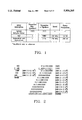
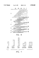
- FIG. 1 gives an idea of the size of 8-bit multipliers. With VLSI (Very Large Scale Integration) systems becoming commonplace and multi-million transistor circuits no longer rare, the problem has been reduced to that of mastering the Boolean expressions.
- Modern digital computers are often rated by how many mathematical operations they can perform in a given time (e.g. MFLOPS, or Millions of Floating Point operations per second). Of these millions of operations, multiplication and division are the most time consuming. In counting normalized floating point operations per second, multiplication is given a weight of 4 times that of addition.
- C. S. Wallace claimed that the arithmetic unit of a computer "used for scientific computations, will spend nearly half of its time multiplying or dividing".
- C. S. Wallace "A Suggestion for a Fast Multiplier," IEEE Transactions on Electronic Computers, Volume 13, pp. 14-17, February 1964. The processes of multiplication and division have remained key topics for research throughout the history of the computer.
- the first multiplication methods used with computers and calculating machines were, in nature, algorithms.
- the iterative addition method simply adds the multiplicand to itself as many times as the multiplier dictates. This method requires minimal code to implement and only one carry bit per iteration.
- Mechanical accounting machines utilized a hardware realization of this method for multiplication. Obviously this process can be extremely slow for large numbers.
- the second method is based on the system used for multiplying decimal numbers.
- Each digit of the multiplier operates on the entire multiplicand to produce intermediate terms (partial products).
- the partial products from each operation are shifted to the proper location with respect to the exponent value of the multiplier digit, then all the intermediate terms are added to produce the final product.
- C. H. Chen ed.
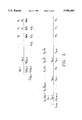
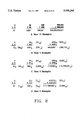
- FIG. 2 demonstrates this technique in identical multiplications, one in decimal, the other in binary.
- This "left shift" multiplication technique requires a more complex algorithm for implementation but offers a great increase in speed over the iterative method since the number of operations is always equal to the number of bits in the operands.
- Left shift arrays can be easily constructed in two parts, a partial product generator; which is simply an array of logical AND gates, and the addition array; which combines all partial products to obtain the final result. Notice, however, that the sign bit is not actually generated by this technique, but must be calculated separately.
- This organizational requirement led Booth, in 1951, A. D. Booth, "A Signed Binary Multiplication Technique," to develop a method that returned the correct two's complement value. Quarterly Journal of Mechanics and Applied Mathematics, Volume 4, number 2, pp. 236-240, 1951.
- Booth's process amounts to adjusting for the correction factor during the multiplication process.
- His correction scheme works by treating each pair of bits as if they represent a magnitude and a sign bit. Using only this idea the algorithm must obey the following conditions: if the more significant of the two bits is a zero, the multiplication is treated as a positive integer multiplication; if the more significant bit is one the multiplication is treated as if needing two's complement correction. The algorithm must also account for the case when two's complement correction occurs unnecessarily. If the more significant bit is zero and the lessor bit is one, the algorithm adjusts for incorrect two's complement correction by adding r back to the sum.
- MacSorley's modified Booths algorithm consists of the following conditions:
- MacSorley's modified algorithm obviously requires only half the iterations as Booth's original algorithm, but suffers from the same constraints.
- an even larger multiplexor must be used for each stage, and each stage depends on the completion of the previous stage.
- FIG. 3 shows the Baugh-Wooley multiplication algorithm.
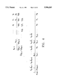
- Wallace first insight was to connect these adders to combine three partial product bits and produce a sum and carry bit that would be reduced in the next addition cycle.
- Pryor to Wallace's work half adders were used to add two partial product bits producing a carry bit and a sum bit. These sum and carry bits would then be added to the correct magnitude bits from the next partial product using full adders (each full adder receiving one carry and two sum inputs). The resulting sum and carries were combined with the next partial product until all terms had been combined. This re-arrangement of the full adder input bits, by itself, reduces the time to add the partial products by a factor of 1.5.
- FIG. 6 shows the reduction of 12-bit partial products using a Wallace tree compose of full and half adders. The brackets at the right denote the terms to be combined each cycle. This example reduces the partial products to two terms for final addition in a CLA in 5 cycles.
- the problem of multiplying binary numbers in computing machines has been studied in great detail in the last fifty years and is well understood.
- the basic binary multiplication technique is similar to the method for multiplying decimal numbers.
- the technique includes the generation of partial products followed by the addition of the partial products to produce the final product.
- Algorithms have been developed to handle 2's complement numbers and to speed the process of adding the partial products.
- all the techniques that have been documented for binary multiplication include the production of partial products and the reduction, or addition, of these intermediate terms to produce the final product.
- a need continues to exist for a multiplier capable of functioning in the quickest manner possible.
- the present invention provides such a multiplier.
- FIG. 1 is a Comparison of 8-bit by 8-bit Multipliers.
- FIG. 2 is a Decimal and Binary "Left-Shift" Multiplication.
- FIG. 3 is a Baugh-Wooley Multiplication Algorithm.
- FIG. 4 is a Modified Baugh-Wooley Multiplication Algorithm.
- FIG. 5 is a Fully Modified Baugh-Wooley Multiplication Algorithm.
- FIG. 6 is a Reduction of Partial Products using a Wallace Tree.
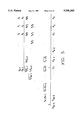
- FIG. 7 is a Generalized Dadda Counters.
- FIG. 8 is an Example of Greatest Magnitude n-digit Multiplication.
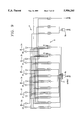
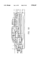
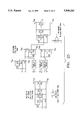
- FIGS. 9-14 are a schematic of an unsigned 4-bit by 4-bit multiplier.
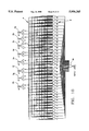
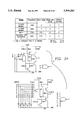
- FIGS. 15-17 are a schematic of the most significant portion of the two's complement (signed multiplier).
- FIG. 18 is a 10-bit by 10-bit Binary Multiplication and Matrix Representation.
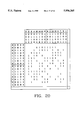
- FIG. 19 is an Alternative Karnaugh Map Example.
- FIG. 20 is a Modified Gray-code Alternative Karnaugh Map Example.
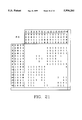
- FIG. 21 is a Two's Complement Alternative Karnaugh Map Example.
- FIG. 22 is a 4-bit Parallel Multiplier without Wallace/Dadda Reduction.
- FIG. 23 is a Comparison of Boolean Multiplier to Baseline Designs.
- FIG. 24 is a Comparison of 2-input and 8-input TTL Gates.
- FIG. 25 is a Comparison of 2-input and 8-input CMOS Gates.
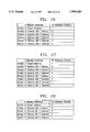
- FIG. 26 is a table of Instances of 4 Element Subterms in 4-bit Unsigned Multiplier.
- FIG. 27 is a table of Instances of 3 Element Subterms in 4-bit Unsigned Multiplier.
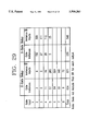
- FIG. 28 is a table of Instances of 2 Element Subterms in 4-bit Unsigned Multiplier.
- FIG. 29 is a labbe of comparison of economy of 2-gate delay and 3-gate delay multiplier.
- the boolean multiplier includes a plurality of input buffers for storing a first operand and a second operand.
- the multiplier also includes a first set of gates coupled to the input buffers, the first set of gates respectively combining the first operand and the second operand with Boolean function to produce logical products.
- the multiplier further includes a second set of gates coupled to the first set of gates, the second set of gates respectively combining the logical products with Boolean functions to produce specific product bits.
- the product bits of a digital multiplier can be produced as Boolean combinations of the inputs (i. e. operand bits).
- the present invention uses these Boolean representation as a method of multiplication, i.e. a Boolean multiplier.
- each output bit is produced independently of, and in parallel with, the production of all other product bits.
- the Boolean multiplier is analogous to the carry-look-ahead adder.
- Boolean method is used to produce a maximum speed multiplier, that is a multiplier with only two gate delays from operand input to product output (not counting term inverters and buffers).
- the 4-bit by 4-bit case (8-bit product), both 2's complement and unsigned binary, are studied to demonstrate the process.
- n-digit number in base x can be expressed as a polynomial of the form:
- a 0 , a 1 , a 2 , ⁇ , a n-1 are digit values in the range 0 ⁇ a ⁇ x-1.
- the polynomial thus formed is:
- x 2n is greater than the result of the greatest magnitude n-digit by n-digit multiplication. Note that this is exclusively greater than. Since we are dealing with integers, the largest term of the n-digit multiplication product is not greater than (x-1)x 2n-1 . Since the largest product term is of the order x 2n-1 , the product of an n-digit by n-digit multiplication is at most 2n digits in size.
- the zeroth or least significant digit is one (1)
- the nth digit (or digit in the x n column) is x-2,
- m represents an (n-1) digit number
- k represents an (n-1) digit number
- k+1 represents a positive number in x's complement format
- a positive number in x's complement format always has a zero as the most significant digit.
- the greatest magnitude positive value that can be expressed in an n-digit x's complement number is x n-1 -1; so that exactly x n-1 -1 positive values can be represented.
- n the total number of values, d, that can be represented is the number of positive values (x n-1 -1) plus the number of negative values (x n-1 ) plus the one zero value which sum to 2 n-1 .
- the number of discrete values in x's complement format, d, is defined in equation (1.8).
- m is an (n-1) bit value.
- the two's complement format as a subset of the x's complement system, is not actually a sign-magnitude format, but a weighted system with the MSB having a negative weight.
- the Multiplicand, A, and Multiplier, B are treated as identical operands.
- the bits of each operand are noted as a 0 , a 1 , . . . a n-1 and b 0 , b 1 , . . . b n-1 , respectively where the subscript refers to the power of 2 so that the least significant bit (LSB) of A is a 0 , and the most significant bit MSB of an n-bit operand B is b n-1 .
- the product, or result is referenced as P with bits p 0 , p 1 , . . . p 2n-1 for the 2n-bit product of an n-bit by n-bit multiplication.
- a dual subscript system is employed where the first subscript refers to the bit size of the word and the second subscript refers to the specific bit.
- b 16 .8 represents the eighth bit of a 16-bit multiplier
- p 32 .7 represents the seventh bit of a 32-bit product (the product of two 16 bit multiplicands).
- the LSB of each operand or product, x 0 will be referred to as the zeroth bit and the x 1 term will be referred to as the first bit, where the subscript refers to the respective exponent of two.
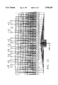
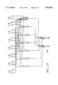
- FIGS. 9-14 are schematics of a multiplier manufactures in accordance with the present invention.
- the schematic demonstrates a multiplier for an unsigned 4-bit by 4-bit multiplier. Accordingly, a 3 , a 2 , a 1 and a 0 respectively represent the input bits of operand A and b 3 , b 2 , b 1 and b 0 respectively represent the input bits.
- the product bits are respectively represented by p 7 , p 6 , p 5 , p 4 , p 3 , p 2 , p 1 and p 0 .
- the multiplier could readily be extended to handle higher level operandi without departing from the spirit of the present invention.
- input signals are provided to input buffers 2a-2h.
- the bits provided to the input buffers are transmitted on a bus 4 to a first set of NAND Gates 6. After passing through the first set of NAND Gates the processed bits are transmitted to a second set of NAND Gates 8a-8g where the bits are final processed to produce specific product bits.
- the NAND/NAND multiplier could be converted to a AND/OR multiplier by replacing the first set of NAND Gates with AND Gates and replacing the second set of NAND Gates to OR Gates. While this conversion would alter the logic of the present invention, it is considered to be within the spirit of the present invention.
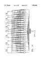
- FIGS. 15-17 disclose a schematic for the most significant portion of the two's complement multiplier (signed multiplier).
- the two's complement includes input buffers for input bits a 3 , a 2 , a 1 , a 0 , b 3 , b 2 , b 1 and b 0 .
- the multiplier also includes first set of NAND Gates and a second set of NAND Gates.
- the second set of NAND Gates produce product bits p 7 , p 6 , p 5 , and p 4 .
- P 3 -P 0 are produced in the same manner as with p 3 -p 0 of the unsigned multiplier shown in FIGS. 9-14. As such, your attention is particularly directed to FIGS. 9-11.
- each term is produced in the 10-bit by 10-bit multiplication example from FIG. 8.
- the example is reproduced in FIG. 18 in binary and matrix representation.
- the matrix representation allows straight forward analysis of the multiplication process and the resulting hardware realization.
- the black dots in the matrix representation denote single bit terms.
- each dot is an input bit (a i or b i ).
- each dot represents the logical AND of two of the input bits.
- the first partial product (for this 9-bit case) is:
- Boolean exclusive-OR (XOR, ⁇ ) function produces the sum bit for each addition.
- Each product bit can then be produced by the XORing of the pertinent intermediate term bits and the proper carry information. This is not necessary for p 0 . Since there is no addition involved in its production; the algorithm still applies to this case.
- the product bits can be expressed as
- Equations (3.2) and (3.4) are sufficient for p 0 and p 1 for any size multiplier, whether 2's complement or unsigned binary.
- Gaskill utilizes equations (3.2), (3.4), and (3.6) for the first three product terms, but never explicitly states equation (3.1). Gaskill also does not attempt to produce the expression in 2-gate delay form. J. R. Gaskill Jr., L. R. Weill, "Four-by-four bit Multiplier Module having Three Stages of Logic Cells," U.S. Pat. No. 3,914,589, October 1975.
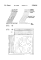
- the K-map generating programs produced a single map for each output term by computing each multiplication and then examining the state of the pertinent bit in the result. For this research, each multiplication was repeated for each K-map. A more efficient approach would have been to compute each multiplication and then extract all the output values before proceeding to the next operation. This alternative method would have required producing multiple output files simultaneously, one for each K-map. Considering the limited number of reasonably sized maps required, the method of producing each K-map separately was acceptable. (More on the size of Karnaugh maps and number of minterms in the Results and Findings section.)
- Equations (3.9)-(3.12) are denoted as p 8 ,y because they each represent a Boolean expression for the yth bit of an 8-bit product (i.e. the product of a 4-bit by 4-bit multiplication). These terms are subsets of expressions for multiplications of higher order. Because of this fact, the equations for the products of order less than n in an n-bit by n-bit multiplication, are universal (equations (3.2), (3.4), (3.7), and (3.8)).
- Equation (3.16) represents the sign bit of the product and are determined by the following rules for multiplying signed numbers:
- the next most significant bit, 2n-2 contains sign extension bits from the MSB and the product term from the most significant negative number multiplication as discussed previously. Because of this, the 2n-2 product bit of an n-bit by n-bit two's complement multiplication can be expressed as:
- Equations (3.17) and (3.18) can be combined to produce a simplified expression for bit 2n-2 of the two's complement product.
- Section D of this section documents a related finding from this research, a mathematical curiosity involving the p 1 bit of the output.
- the Boolean expressions describing this fast multiplier represent a non-cellular, non-symmetrical design.
- the design is also difficult to verify because of the irregular nature of the Boolean expressions.
- These facts describe a complex design when compared to the simple parallel multiplier design.
- the parallel multiplier without Wallace tree reduction, is both cellular and symmetrical but represents a gate delay on the order of 4n for designs using exclusively 2-input gates. This is due to one the gate delay for the partial products, then three gates delays for each carry, propagating from the least significant addition (not the LSB) to the addition that produces the MSB of the product. (A parallel multiplier utlizing three-input gates can be designed with only 3n gate delays.)
- FIG. 22 does not clearly show the symmetry of the parallel multiplier but does confirm that the 4-bit by 4-bit case requires 80 two-input logic gates and produces a delay of at least 16-gates.
- the delay problem in traditional multipliers is complicated by the fact that the most significant digits suffer the longest delay. In multipliers using Wallace/Dadda reduction, the delay is decreased but the most significant bits still have the longest delay. This problem is notable in floating point ALUs (Arithmetic Logic Unit) where bits of lessor significance may be discarded.
- ALUs Arimetic Logic Unit
- a slow (7,3) counter requires at least four times the circuitry and chip area as a (3,2) counter.
- a relatively fast (7, 3) counter requires the XOR of all inputs to product the least significant output (s 0 ), the XOR of 21 two-digit AND terms for s 1 , and the OR of 35 four digit AND terms for s 2 . This problem has led to research in the area of majority gates. The decision for designers to consider is not between slow, low gate count parallel multipliers and the Boolean design, but between fast complex pipelined multipliers and the larger, faster Boolean multiplier design.
- the Boolean multiplier depends upon the use of up to 2n-input AND gates with large OR gate combinations. These devices exist and are at least as space efficient (per input) as two-input gates. Eight-input TTL gates do not require much more space than two-input versions because of the use of diodes to the input transistor (see FIG. 24).
- an eight-input gate requires approximately 30-50% more space than a two-input gate of the same function (a 300% increase in capability).
- CMOS grows nearly linearly with the addition of inputs to a gate (see FIG. 25).
- CMOS Logic Data pp 6-5 to 6-11, Motorola Inc., Phoenix, Ariz., 1991.
- the average transistor count is four transistors per input. An approximation of four transistors per input per gate is reasonable based on these comparisons. Propagation delays are the same, in both CMOS and TTL, for large (eight-input) or small (two-input) gates of the same function.
- Timing delays for this work are based on switching propagation delay of logical gates being constant. Within a logic technology, this assumption is usually accepted.
- a subterm be the part of a logical term that is contributed from one operand.
- a 3 a 2 is the a-subterm
- b 3 b 2 b 0 is the b-subterm.
- the Boolean expressions defined in equations (3.7) through (3.16) can be expressed as sets of ANDed subterms, thus adding one gate delay and eliminating the need for AND gates with more than five inputs.
- FIGS. 26-28 show the results of investigating the occurrences of the various subterms. In these tables, all the possible subterms for the element size are accounted for and categorized by the number of instances. The number of instances of each subtem dictates the area economy to be gained by grouping terms.
- a comparison of transistor count was produced using the approximation of four transistors per input per gate and compared to baseline designs in FIG. 23.
- the multipliers listed in FIG. 1 were used as baseline for existing designs.
- the two logic level Boolean multiplier would require 4,156 transistors to realize, or slightly more than triple the chip area.
- the three logic level Boolean multiplier requires 2,864 transistors or more than double the area of the baseline designs. Both baseline designs rely on pipelining to achieve high throughput and actually have a gate delay of order 4n, for an n-bit input, for the first multiplication product. Table 4.5 directly compares the designs.
- Another useful approach is to incorporate selected parts of the Boolean multiplier into a conventional multiplier. If the Boolean expressions are used only for the most significant digits, a moderate speed increase can be realized without as great an increase in area as using the full Boolean approach. Hybridizing the multiplier is attractive because of the great improvement in returning the MSB.
- a Karnaugh map accounts for every possible input combination for a set of digital inputs. For an n-bit by n-bit multiplier, there are 2n inputs and 2n outputs. Each output bit represents one expression and therefore one Karnaugh map.
- the number of inputs for a term, and its related K-map, is determined either by the multiplier size or the significance of the product bit, whichever is larger. Where x is the number of input bits for product term p i :
- n-1 lessor order bits are either defined from multipliers with lower bit count, or can be derived with a smaller K-map.
- this discussion will concentrate on the n+1 maps with 2n inputs, also referred to as complete maps.
- Each of these maps display 2 2n minterms, requiring 2 2n multiplications to complete.
- the number of multiplications required and the size of the maps is trivial.
- the 8-bit cases were computed, although the Boolean expressions have not been derived for this case. The problem of magnitude becomes obvious when considering the 8-bit Kamaugh maps with 65536 minterms each. Even this magnitude seems insignificant when compared to a 32-bit multiplier that requires over 18 ⁇ 10 18 multiplications just to populate the K-maps.
- each complete product term, p n is the sum of n+1 partial product bits and .left brkt-bot.log 2 n.right brkt-bot. carry terms.
- the minimum number of product terms, t n to be ORed together in the flattened expression is:
- Equation (4.6) is based on the expansion of the XOR operation on simple terms.
- the carry terms usually have multiple elements ORed together, each element having multiple subterms.
- a possible alternative is to pursue four logic level Boolean multiplier designs, or even designs with more than four gate delays.
- Splitting a long XOR expression before flattening yields two much more efficient expressions to be XORed for the final output (three logic levels).
- Dividing a large product expression (based on equation (3.1)) into four manageable pieces reduces the complexity of the circuit by orders of magnitude while only adding two gate delays. Because of the relationship of the number of XORs to the number of terms in the final expression, flattening pieces of the total product expression reduces complexity significantly for each level of delay added.
- Boolean multipliers with more logic levels can still achieve the goal of a single-cycle multiplier. Techniques and algorithms for producing the most efficient four gate delay expression would have to be developed.
- This theorem makes designing a digital squaring device a little simpler.
- the PIC series of microprocessors produced by Microchip Corporation has not included a device with a multiplier until recently. Even when the need for built-in multiplication capability arises, designs exist for 8-bit multipliers that can produce a result in a single clock cycle at 5 MHz (200 ns).
- MCM Multi-Chip Modules
- systolic arrays and digital neural networks could realize an improvement in throughput due to the heavy dependence on multipliers in these systems.
- the Boolean multiplier, or a hybrid multiplier could even find a niche in engineering workstations and high-end personal computers.
- Applications like finite element analysis (FEA) and computer automated design (CAD) often contain routines that may take hours to run.
- FEA finite element analysis
- CAD computer automated design
- most of the delay is created by the iterative nature of the algorithms adjusting each element to reflect the values of its immediate neighbors, a process that is heavily multiplication dependent.
- Boolean multipliers once developed, could reside on a separate chip inside an MCM with the processor. MCMs are now being experimented with as a possible packaging standard for future processors.
- the inverse of multiplication is a prime candidate for reduction to Boolean terms. Division, although not usually considered a discrete operation, actually also has a finite number of possibilities for and n-bit by n-bit input. If the most significant digits of the operands are aligned, the number of possibilities is reduced by eliminating leading zeros (or leading ones for negative two's complement numbers). Karnaugh maps can be produced for small word size dividers just as easily as for small word size multipliers. Additional bits of accuracy is only a matter of producing more K-maps.
- division is a compare and subtract process, where multiplication is based on an AND then add process. Because of this, the problem of Boolean division probably explodes in the same manner as Boolean multiplication.
- a Boolean equation generating program is also be possible for division.
- Carry-Look-Ahead adders are prime candidates for true Boolean representation.
- An n-bit by n-bit adder only requires n+1 outputs and therefore only n+1 Karnaugh maps, with only the two most significant having 2 2n terms.
- a two gate delay adder could be used not only as an improved adder, but also to improve Wallace tree reduction of partial products in state of the art multipliers.
- This design is a fast digital multiplier for 4-bit (or smaller) binary numbers, both unsigned and signed numbers (in two's complement format) may be multiplied by the two designed described.
- the designs share the least significant nibble (LSN), but have different most significant nibbles (MSN).
- This design represents the fastest possible multiplier (two gate delays, or two logic levels) for 4-bit by 4-bit multiplication. Because of the limits of basic Boolean functions and digital logic gates, a one gate delay multiplier is impossible, hence, this design represents the fastest possible multiplier.
- the part of this device that produces the least significant nibble product (the four lesser significant bit products, expressed as p 0 , p 1 , p 2 and p 3 ) is valid for all unsigned multiplications, regardless of operand size and is valid for all two's complement multiplications with operandi of 4-bit size and larger. This allows this part of the device to be used in larger bit size fast multipliers.
- Equations are defined that describe the construction of fastest possible devices to produce the MSB (Most Significant Bit) and NMSB (Next Most Significant Bit) products for all two's complement multipliers. This part of the multiplier is applicable to all two's complement multipliers. (This claim may not be patentable based on the Gaskill patent. Gaskill gave similar equations, but the Gaskill equations are not correct
- This device produces the multiplication products without generating partial products and produces every product bit independently. This allows parts of the device to be used to produce individual product bits, if necessary, without producing unneeded terms and partial products.
- the device represents a divergence from current design methodology in that partial products are not generated and then added. Instead, the device is based on the Boolean expression for each product bit.
Landscapes
- Physics & Mathematics (AREA)
- General Physics & Mathematics (AREA)
- Computational Mathematics (AREA)
- Mathematical Analysis (AREA)
- Mathematical Optimization (AREA)
- Pure & Applied Mathematics (AREA)
- Engineering & Computer Science (AREA)
- Theoretical Computer Science (AREA)
- Computing Systems (AREA)
- General Engineering & Computer Science (AREA)
- Complex Calculations (AREA)
Abstract
Description
-m=2.sup.n -m (1.1)
m×r=mr (2.1)
(-m)×r=r(2.sup.n -m)=2.sup.n r-mr (2.2)
m×(-r)=m(2.sup.n -r)=2.sup.n m-mr (2.3)
(-m)×(-r)=(2.sup.n -m)(2.sup.n -r)=2.sup.2n -2.sup.n m-2.sup.n r+mr(2.4)
a.sub.0 x.sup.n-1 +a.sub.1 x.sup.n-2 ++a.sub.n-2 x.sup.1 +a.sub.n-1 x.sup.0 (1.1)
ax.sup.n-1 +ax.sup.n-2 ++ax.sup.1 +ax.sup.0 =x.sup.n -1, when a=x-1 (1.2)
x.sup.n >x.sup.n -1=ax.sup.n-1 +ax.sup.n-2 ++ax.sup.1 +ax.sup.0(1.3)
(x.sup.n -1)(x.sup.n -1)=x.sup.2n -2x.sup.n +1 (1.4)
+m=m (1.5)
-m=x.sup.n -m (1.6)
x.sup.n -x.sup.n-1 =(x-1) x.sup.n-1 (1.7)
d=(x.sup.n-1 -1)+x.sup.n-1 +1=2x.sup.n-1 (1.8)
+m=m (1.9)
-m=2.sup.n -m (1.10)
(-2.sup.n-1)×(-2.sup.n-1)=+2.sup.2n-2. (1.11)
p.sub.n =a.sub.0 b.sub.n ⊕a.sub.1 b.sub.n-1 ⊕ . . . ⊕a.sub.n-1 b.sub.1 ⊕a.sub.n b.sub.0 ⊕c.sub.n-1,n ⊕c.sub.n-2,n ⊕ . . . ⊕ c.sub.1,n (3.1)
p.sub.0 =a.sub.0 b.sub.0 (3.2)
c.sub.0 =0 (3.3)
p.sub.1 =a.sub.0 b.sub.1 ⊕a.sub.1 b.sub.0 (3.4)
c.sub.1,2 =a.sub.0 a.sub.1 b.sub.0 b.sub.1 (3.5)
p.sub.2 =a.sub.0 b.sub.2 ⊕a.sub.1 b.sub.1 ⊕a.sub.2 b.sub.0 ⊕a.sub.0 a.sub.1 b.sub.0 b.sub.1 (3.6)
p.sup...sub.2n,2n-1 =a.sub.n-1 b.sub.n-1 (b.sub.n-2 +b.sub.n-3 + . . . +b.sub.1 +b.sub.0)+a.sub.n-1 b.sub.n-1 (a.sub.n-2 +a.sub.n-3 + . . . +a.sub.1 +a.sub.0) (3.17)
p.sup...sub.2n,2n-2 =a.sub.n-1 b.sub.n-1 (b.sub.n-2 +b.sub.n-3 + . . . +b.sub.0)+a.sub.n-1 b.sub.n-1 (a.sub.n-2 +a.sub.n-3 + . . . +a.sub.0) +a.sub.n-1 a.sub.n-2 a.sub.n-3 . . . a.sub.1 a.sub.0 b.sub.n-1 b.sub.n-2 b.sub.n-3 . . . b.sub.1 b.sub.0 (3.18)
p.sup...sub.2n,2n-2 =p.sup...sub.2n,2n-1 +a.sub.n-1 a.sub.n-2 a.sub.n-3 . . . a.sub.1 a.sub.0 b.sub.n-1 b.sub.n-2 b.sub.n-3 . . . b.sub.1 b.sub.0 (3.19)
x=minimum(2(i+1), 2n) (4.2)
x=minimum(2(i+1), 2n) (4.2)
m=(n+1)2.sup.2n (4.3)
A⊕B=AB+AB (4.4)
A⊕B⊕C=ABC+ABC+ABC+ABC (4.5)
A⊕B⊕C⊕D=ABCD+ABCD+ABCD+ABCD+ABCD+ABCD+ABCD+ABCD(4.6)
t.sub.n ≧2.sup.(n+.left brkt-bot.log.sbsp.2.sup.n.right brkt-bot.)(4.7)
p.sub.1 =a.sub.0 b.sub.1 ⊕a.sub.1 b.sub.0 (3.4)
p.sub.1 =a.sub.0 a.sub.1 ⊕a.sub.1 a.sub.0 =0 (4.8)
Claims (20)
p.sup...sub.2n,2n-1 =a.sub.n-1 b.sub.n-1 (b.sub.n-2 +b.sub.n-3 + . . . +b.sub.1 +b.sub.0)+a.sub.n-1 b.sub.n-1 (a.sub.n-2 +a.sub.n-3 + . . . +a.sub.1 +a.sub.0)
p.sup...sub.2n,2n-2 =p.sup...sub.2n,2n-1 +a.sub.n-1 a.sub.n-2 a.sub.n-3 . . . a.sub.1 a.sub.0 b.sub.n-1 b.sub.n-2 b.sub.n-3 . . . b.sub.1 b.sub.0
p.sup...sub.2n,2n-2 =a.sub.n-1 b.sub.n-1 (b.sub.n-2 +b.sub.n-3 + . . . +b.sub.0)+a.sub.n-1 b.sub.n-1 (a.sub.n-2 +a.sub.n-3 + . . . +a.sub.0) +a.sub.n-1 a.sub.n-2 a.sub.n-3 . . . a.sub.1 a.sub.0 b.sub.n-1 b.sub.n-2 b.sub.n-3 . . . b.sub.1 b.sub.0
p.sup...sub.2n,2n-1 =a.sub.n-1 b.sub.n-1 (b.sub.n-2 +b.sub.n-3 + . . . +b.sub.1 +b.sub.0)+a.sub.n-1 b.sub.n-1 (a.sub.n-2 +a.sub.n-3 + . . . +a.sub.1 +a.sub.0)
Priority Applications (1)
| Application Number | Priority Date | Filing Date | Title |
|---|---|---|---|
| US08/863,588 US5956265A (en) | 1996-06-07 | 1997-05-27 | Boolean digital multiplier |
Applications Claiming Priority (2)
| Application Number | Priority Date | Filing Date | Title |
|---|---|---|---|
| US1928996P | 1996-06-07 | 1996-06-07 | |
| US08/863,588 US5956265A (en) | 1996-06-07 | 1997-05-27 | Boolean digital multiplier |
Publications (1)
| Publication Number | Publication Date |
|---|---|
| US5956265A true US5956265A (en) | 1999-09-21 |
Family
ID=26692083
Family Applications (1)
| Application Number | Title | Priority Date | Filing Date |
|---|---|---|---|
| US08/863,588 Expired - Lifetime US5956265A (en) | 1996-06-07 | 1997-05-27 | Boolean digital multiplier |
Country Status (1)
| Country | Link |
|---|---|
| US (1) | US5956265A (en) |
Cited By (63)
| Publication number | Priority date | Publication date | Assignee | Title |
|---|---|---|---|---|
| US6337544B1 (en) * | 1999-12-14 | 2002-01-08 | Philips Electronics North America Corporation | Digital lamp signal processor |
| US6369725B1 (en) * | 2000-09-26 | 2002-04-09 | International Business Machines Corporation | Method for binary to decimal conversion |
| US20040010536A1 (en) * | 2002-07-11 | 2004-01-15 | International Business Machines Corporation | Apparatus for multiplication of data in two's complement and unsigned magnitude formats |
| US20040024804A1 (en) * | 2000-02-21 | 2004-02-05 | Zeng Richard B. | Linear summation multiplier array implementation for both signed and unsigned multiplication |
| US20040054707A1 (en) * | 2001-05-15 | 2004-03-18 | Katsushi Yamada | Multiplication coefficient supplement device, multiplication coefficient supplement method, and multiplication factor supplement program |
| US20040199560A1 (en) * | 2003-04-04 | 2004-10-07 | Vincent Dupaquis | Combined polynomial and natural multiplier architecture |
| US7119576B1 (en) | 2000-09-18 | 2006-10-10 | Altera Corporation | Devices and methods with programmable logic and digital signal processing regions |
| US7346644B1 (en) | 2000-09-18 | 2008-03-18 | Altera Corporation | Devices and methods with programmable logic and digital signal processing regions |
| US20090292756A1 (en) * | 2008-05-23 | 2009-11-26 | Elliot Gibson D | Large-factor multiplication in an array of processors |
| US7814137B1 (en) | 2007-01-09 | 2010-10-12 | Altera Corporation | Combined interpolation and decimation filter for programmable logic device |
| US7822799B1 (en) | 2006-06-26 | 2010-10-26 | Altera Corporation | Adder-rounder circuitry for specialized processing block in programmable logic device |
| US7836117B1 (en) | 2006-04-07 | 2010-11-16 | Altera Corporation | Specialized processing block for programmable logic device |
| US7865541B1 (en) | 2007-01-22 | 2011-01-04 | Altera Corporation | Configuring floating point operations in a programmable logic device |
| US7930336B2 (en) | 2006-12-05 | 2011-04-19 | Altera Corporation | Large multiplier for programmable logic device |
| US7949699B1 (en) | 2007-08-30 | 2011-05-24 | Altera Corporation | Implementation of decimation filter in integrated circuit device using ram-based data storage |
| US7948267B1 (en) | 2010-02-09 | 2011-05-24 | Altera Corporation | Efficient rounding circuits and methods in configurable integrated circuit devices |
| US8041759B1 (en) | 2006-02-09 | 2011-10-18 | Altera Corporation | Specialized processing block for programmable logic device |
| US8244789B1 (en) | 2008-03-14 | 2012-08-14 | Altera Corporation | Normalization of floating point operations in a programmable integrated circuit device |
| US8255448B1 (en) | 2008-10-02 | 2012-08-28 | Altera Corporation | Implementing division in a programmable integrated circuit device |
| US8266199B2 (en) | 2006-02-09 | 2012-09-11 | Altera Corporation | Specialized processing block for programmable logic device |
| US8266198B2 (en) | 2006-02-09 | 2012-09-11 | Altera Corporation | Specialized processing block for programmable logic device |
| US8301681B1 (en) | 2006-02-09 | 2012-10-30 | Altera Corporation | Specialized processing block for programmable logic device |
| US8307023B1 (en) | 2008-10-10 | 2012-11-06 | Altera Corporation | DSP block for implementing large multiplier on a programmable integrated circuit device |
| US8386550B1 (en) | 2006-09-20 | 2013-02-26 | Altera Corporation | Method for configuring a finite impulse response filter in a programmable logic device |
| US8386553B1 (en) | 2006-12-05 | 2013-02-26 | Altera Corporation | Large multiplier for programmable logic device |
| US8396914B1 (en) | 2009-09-11 | 2013-03-12 | Altera Corporation | Matrix decomposition in an integrated circuit device |
| US8412756B1 (en) | 2009-09-11 | 2013-04-02 | Altera Corporation | Multi-operand floating point operations in a programmable integrated circuit device |
| US8458243B1 (en) | 2010-03-03 | 2013-06-04 | Altera Corporation | Digital signal processing circuit blocks with support for systolic finite-impulse-response digital filtering |
| US8468192B1 (en) | 2009-03-03 | 2013-06-18 | Altera Corporation | Implementing multipliers in a programmable integrated circuit device |
| US8484265B1 (en) | 2010-03-04 | 2013-07-09 | Altera Corporation | Angular range reduction in an integrated circuit device |
| US8510354B1 (en) | 2010-03-12 | 2013-08-13 | Altera Corporation | Calculation of trigonometric functions in an integrated circuit device |
| US8539014B2 (en) | 2010-03-25 | 2013-09-17 | Altera Corporation | Solving linear matrices in an integrated circuit device |
| US8539016B1 (en) | 2010-02-09 | 2013-09-17 | Altera Corporation | QR decomposition in an integrated circuit device |
| US8543634B1 (en) | 2012-03-30 | 2013-09-24 | Altera Corporation | Specialized processing block for programmable integrated circuit device |
| US8549055B2 (en) | 2009-03-03 | 2013-10-01 | Altera Corporation | Modular digital signal processing circuitry with optionally usable, dedicated connections between modules of the circuitry |
| US8577951B1 (en) | 2010-08-19 | 2013-11-05 | Altera Corporation | Matrix operations in an integrated circuit device |
| US8589463B2 (en) | 2010-06-25 | 2013-11-19 | Altera Corporation | Calculation of trigonometric functions in an integrated circuit device |
| US8601044B2 (en) | 2010-03-02 | 2013-12-03 | Altera Corporation | Discrete Fourier Transform in an integrated circuit device |
| US8620980B1 (en) | 2005-09-27 | 2013-12-31 | Altera Corporation | Programmable device with specialized multiplier blocks |
| US8626815B1 (en) | 2008-07-14 | 2014-01-07 | Altera Corporation | Configuring a programmable integrated circuit device to perform matrix multiplication |
| US8645449B1 (en) | 2009-03-03 | 2014-02-04 | Altera Corporation | Combined floating point adder and subtractor |
| US8645451B2 (en) | 2011-03-10 | 2014-02-04 | Altera Corporation | Double-clocked specialized processing block in an integrated circuit device |
| US8645450B1 (en) | 2007-03-02 | 2014-02-04 | Altera Corporation | Multiplier-accumulator circuitry and methods |
| US8650231B1 (en) | 2007-01-22 | 2014-02-11 | Altera Corporation | Configuring floating point operations in a programmable device |
| US8650236B1 (en) | 2009-08-04 | 2014-02-11 | Altera Corporation | High-rate interpolation or decimation filter in integrated circuit device |
| US8706790B1 (en) | 2009-03-03 | 2014-04-22 | Altera Corporation | Implementing mixed-precision floating-point operations in a programmable integrated circuit device |
| US8762443B1 (en) | 2011-11-15 | 2014-06-24 | Altera Corporation | Matrix operations in an integrated circuit device |
| US8805916B2 (en) | 2009-03-03 | 2014-08-12 | Altera Corporation | Digital signal processing circuitry with redundancy and bidirectional data paths |
| US8812576B1 (en) | 2011-09-12 | 2014-08-19 | Altera Corporation | QR decomposition in an integrated circuit device |
| US8862650B2 (en) | 2010-06-25 | 2014-10-14 | Altera Corporation | Calculation of trigonometric functions in an integrated circuit device |
| US8886696B1 (en) | 2009-03-03 | 2014-11-11 | Altera Corporation | Digital signal processing circuitry with redundancy and ability to support larger multipliers |
| US8949298B1 (en) | 2011-09-16 | 2015-02-03 | Altera Corporation | Computing floating-point polynomials in an integrated circuit device |
| US8959137B1 (en) | 2008-02-20 | 2015-02-17 | Altera Corporation | Implementing large multipliers in a programmable integrated circuit device |
| US8996600B1 (en) | 2012-08-03 | 2015-03-31 | Altera Corporation | Specialized processing block for implementing floating-point multiplier with subnormal operation support |
| US9053045B1 (en) | 2011-09-16 | 2015-06-09 | Altera Corporation | Computing floating-point polynomials in an integrated circuit device |
| US9098332B1 (en) | 2012-06-01 | 2015-08-04 | Altera Corporation | Specialized processing block with fixed- and floating-point structures |
| US9189200B1 (en) | 2013-03-14 | 2015-11-17 | Altera Corporation | Multiple-precision processing block in a programmable integrated circuit device |
| US9207909B1 (en) | 2012-11-26 | 2015-12-08 | Altera Corporation | Polynomial calculations optimized for programmable integrated circuit device structures |
| US9348795B1 (en) | 2013-07-03 | 2016-05-24 | Altera Corporation | Programmable device using fixed and configurable logic to implement floating-point rounding |
| US9379687B1 (en) | 2014-01-14 | 2016-06-28 | Altera Corporation | Pipelined systolic finite impulse response filter |
| US9600278B1 (en) | 2011-05-09 | 2017-03-21 | Altera Corporation | Programmable device using fixed and configurable logic to implement recursive trees |
| US9684488B2 (en) | 2015-03-26 | 2017-06-20 | Altera Corporation | Combined adder and pre-adder for high-radix multiplier circuit |
| US10942706B2 (en) | 2017-05-05 | 2021-03-09 | Intel Corporation | Implementation of floating-point trigonometric functions in an integrated circuit device |
Citations (16)
| Publication number | Priority date | Publication date | Assignee | Title |
|---|---|---|---|---|
| US3610907A (en) * | 1969-01-16 | 1971-10-05 | North American Rockwell | Multipurpose serial/parallel multiplier |
| US3610906A (en) * | 1968-11-07 | 1971-10-05 | Burroughs Corp | Binary multiplication utilizing squaring techniques |
| US3617723A (en) * | 1970-02-25 | 1971-11-02 | Collins Radio Co | Digitalized multiplier |
| US3805037A (en) * | 1972-02-22 | 1974-04-16 | J Ellison | N{40 th power galois linear gate |
| US3914589A (en) * | 1974-05-13 | 1975-10-21 | Hughes Aircraft Co | Four-by-four bit multiplier module having three stages of logic cells |
| US4013879A (en) * | 1975-06-02 | 1977-03-22 | International Telephone And Telegraph Corporation | Digital multiplier |
| US4086657A (en) * | 1976-08-18 | 1978-04-25 | The United States Of America As Represented By The Secretary Of The Air Force | Five-stage four-bit complex multiplier |
| US4130877A (en) * | 1977-01-24 | 1978-12-19 | Westinghouse Electric Corp. | Binary multiplier using identical memories or identical networks |
| US4130878A (en) * | 1978-04-03 | 1978-12-19 | Motorola, Inc. | Expandable 4 × 8 array multiplier |
| US4190894A (en) * | 1978-03-10 | 1980-02-26 | Digital Equipment Corporation | High speed parallel multiplication apparatus with single-step summand reduction |
| US4216531A (en) * | 1978-11-17 | 1980-08-05 | Control Data Corporation | Finite field multiplier |
| US4251875A (en) * | 1979-02-12 | 1981-02-17 | Sperry Corporation | Sequential Galois multiplication in GF(2n) with GF(2m) Galois multiplication gates |
| US4941121A (en) * | 1988-04-01 | 1990-07-10 | Digital Equipment Corporation | Apparatus for high performance multiplication |
| US4967107A (en) * | 1989-05-12 | 1990-10-30 | Plus Logic, Inc. | Programmable logic expander |
| US5175862A (en) * | 1989-12-29 | 1992-12-29 | Supercomputer Systems Limited Partnership | Method and apparatus for a special purpose arithmetic boolean unit |
| US5438533A (en) * | 1992-10-28 | 1995-08-01 | Sharp Kabushiki Kaisha | Multivalued multiplier for binary and multivalued logic data |
-
1997
- 1997-05-27 US US08/863,588 patent/US5956265A/en not_active Expired - Lifetime
Patent Citations (16)
| Publication number | Priority date | Publication date | Assignee | Title |
|---|---|---|---|---|
| US3610906A (en) * | 1968-11-07 | 1971-10-05 | Burroughs Corp | Binary multiplication utilizing squaring techniques |
| US3610907A (en) * | 1969-01-16 | 1971-10-05 | North American Rockwell | Multipurpose serial/parallel multiplier |
| US3617723A (en) * | 1970-02-25 | 1971-11-02 | Collins Radio Co | Digitalized multiplier |
| US3805037A (en) * | 1972-02-22 | 1974-04-16 | J Ellison | N{40 th power galois linear gate |
| US3914589A (en) * | 1974-05-13 | 1975-10-21 | Hughes Aircraft Co | Four-by-four bit multiplier module having three stages of logic cells |
| US4013879A (en) * | 1975-06-02 | 1977-03-22 | International Telephone And Telegraph Corporation | Digital multiplier |
| US4086657A (en) * | 1976-08-18 | 1978-04-25 | The United States Of America As Represented By The Secretary Of The Air Force | Five-stage four-bit complex multiplier |
| US4130877A (en) * | 1977-01-24 | 1978-12-19 | Westinghouse Electric Corp. | Binary multiplier using identical memories or identical networks |
| US4190894A (en) * | 1978-03-10 | 1980-02-26 | Digital Equipment Corporation | High speed parallel multiplication apparatus with single-step summand reduction |
| US4130878A (en) * | 1978-04-03 | 1978-12-19 | Motorola, Inc. | Expandable 4 × 8 array multiplier |
| US4216531A (en) * | 1978-11-17 | 1980-08-05 | Control Data Corporation | Finite field multiplier |
| US4251875A (en) * | 1979-02-12 | 1981-02-17 | Sperry Corporation | Sequential Galois multiplication in GF(2n) with GF(2m) Galois multiplication gates |
| US4941121A (en) * | 1988-04-01 | 1990-07-10 | Digital Equipment Corporation | Apparatus for high performance multiplication |
| US4967107A (en) * | 1989-05-12 | 1990-10-30 | Plus Logic, Inc. | Programmable logic expander |
| US5175862A (en) * | 1989-12-29 | 1992-12-29 | Supercomputer Systems Limited Partnership | Method and apparatus for a special purpose arithmetic boolean unit |
| US5438533A (en) * | 1992-10-28 | 1995-08-01 | Sharp Kabushiki Kaisha | Multivalued multiplier for binary and multivalued logic data |
Cited By (73)
| Publication number | Priority date | Publication date | Assignee | Title |
|---|---|---|---|---|
| US6337544B1 (en) * | 1999-12-14 | 2002-01-08 | Philips Electronics North America Corporation | Digital lamp signal processor |
| US20040024804A1 (en) * | 2000-02-21 | 2004-02-05 | Zeng Richard B. | Linear summation multiplier array implementation for both signed and unsigned multiplication |
| US7346644B1 (en) | 2000-09-18 | 2008-03-18 | Altera Corporation | Devices and methods with programmable logic and digital signal processing regions |
| US7119576B1 (en) | 2000-09-18 | 2006-10-10 | Altera Corporation | Devices and methods with programmable logic and digital signal processing regions |
| US6369725B1 (en) * | 2000-09-26 | 2002-04-09 | International Business Machines Corporation | Method for binary to decimal conversion |
| US20040054707A1 (en) * | 2001-05-15 | 2004-03-18 | Katsushi Yamada | Multiplication coefficient supplement device, multiplication coefficient supplement method, and multiplication factor supplement program |
| US20040010536A1 (en) * | 2002-07-11 | 2004-01-15 | International Business Machines Corporation | Apparatus for multiplication of data in two's complement and unsigned magnitude formats |
| US20040199560A1 (en) * | 2003-04-04 | 2004-10-07 | Vincent Dupaquis | Combined polynomial and natural multiplier architecture |
| US7266579B2 (en) * | 2003-04-04 | 2007-09-04 | Atmel Corporation | Combined polynomial and natural multiplier architecture |
| US8620980B1 (en) | 2005-09-27 | 2013-12-31 | Altera Corporation | Programmable device with specialized multiplier blocks |
| US8041759B1 (en) | 2006-02-09 | 2011-10-18 | Altera Corporation | Specialized processing block for programmable logic device |
| US8301681B1 (en) | 2006-02-09 | 2012-10-30 | Altera Corporation | Specialized processing block for programmable logic device |
| US8266198B2 (en) | 2006-02-09 | 2012-09-11 | Altera Corporation | Specialized processing block for programmable logic device |
| US8266199B2 (en) | 2006-02-09 | 2012-09-11 | Altera Corporation | Specialized processing block for programmable logic device |
| US7836117B1 (en) | 2006-04-07 | 2010-11-16 | Altera Corporation | Specialized processing block for programmable logic device |
| US7822799B1 (en) | 2006-06-26 | 2010-10-26 | Altera Corporation | Adder-rounder circuitry for specialized processing block in programmable logic device |
| US8386550B1 (en) | 2006-09-20 | 2013-02-26 | Altera Corporation | Method for configuring a finite impulse response filter in a programmable logic device |
| US8788562B2 (en) | 2006-12-05 | 2014-07-22 | Altera Corporation | Large multiplier for programmable logic device |
| US9395953B2 (en) | 2006-12-05 | 2016-07-19 | Altera Corporation | Large multiplier for programmable logic device |
| US8386553B1 (en) | 2006-12-05 | 2013-02-26 | Altera Corporation | Large multiplier for programmable logic device |
| US7930336B2 (en) | 2006-12-05 | 2011-04-19 | Altera Corporation | Large multiplier for programmable logic device |
| US9063870B1 (en) | 2006-12-05 | 2015-06-23 | Altera Corporation | Large multiplier for programmable logic device |
| US7814137B1 (en) | 2007-01-09 | 2010-10-12 | Altera Corporation | Combined interpolation and decimation filter for programmable logic device |
| US8650231B1 (en) | 2007-01-22 | 2014-02-11 | Altera Corporation | Configuring floating point operations in a programmable device |
| US7865541B1 (en) | 2007-01-22 | 2011-01-04 | Altera Corporation | Configuring floating point operations in a programmable logic device |
| US8645450B1 (en) | 2007-03-02 | 2014-02-04 | Altera Corporation | Multiplier-accumulator circuitry and methods |
| US7949699B1 (en) | 2007-08-30 | 2011-05-24 | Altera Corporation | Implementation of decimation filter in integrated circuit device using ram-based data storage |
| US8959137B1 (en) | 2008-02-20 | 2015-02-17 | Altera Corporation | Implementing large multipliers in a programmable integrated circuit device |
| US8244789B1 (en) | 2008-03-14 | 2012-08-14 | Altera Corporation | Normalization of floating point operations in a programmable integrated circuit device |
| US8886695B1 (en) | 2008-03-14 | 2014-11-11 | Altera Corporation | Normalization of floating point operations in a programmable integrated circuit device |
| US20090292756A1 (en) * | 2008-05-23 | 2009-11-26 | Elliot Gibson D | Large-factor multiplication in an array of processors |
| US8626815B1 (en) | 2008-07-14 | 2014-01-07 | Altera Corporation | Configuring a programmable integrated circuit device to perform matrix multiplication |
| US8255448B1 (en) | 2008-10-02 | 2012-08-28 | Altera Corporation | Implementing division in a programmable integrated circuit device |
| US8307023B1 (en) | 2008-10-10 | 2012-11-06 | Altera Corporation | DSP block for implementing large multiplier on a programmable integrated circuit device |
| US8549055B2 (en) | 2009-03-03 | 2013-10-01 | Altera Corporation | Modular digital signal processing circuitry with optionally usable, dedicated connections between modules of the circuitry |
| US8706790B1 (en) | 2009-03-03 | 2014-04-22 | Altera Corporation | Implementing mixed-precision floating-point operations in a programmable integrated circuit device |
| US8645449B1 (en) | 2009-03-03 | 2014-02-04 | Altera Corporation | Combined floating point adder and subtractor |
| US8751551B2 (en) | 2009-03-03 | 2014-06-10 | Altera Corporation | Modular digital signal processing circuitry with optionally usable, dedicated connections between modules of the circuitry |
| US8468192B1 (en) | 2009-03-03 | 2013-06-18 | Altera Corporation | Implementing multipliers in a programmable integrated circuit device |
| US8886696B1 (en) | 2009-03-03 | 2014-11-11 | Altera Corporation | Digital signal processing circuitry with redundancy and ability to support larger multipliers |
| US8620977B1 (en) | 2009-03-03 | 2013-12-31 | Altera Corporation | Modular digital signal processing circuitry with optionally usable, dedicated connections between modules of the circuitry |
| US8805916B2 (en) | 2009-03-03 | 2014-08-12 | Altera Corporation | Digital signal processing circuitry with redundancy and bidirectional data paths |
| US8650236B1 (en) | 2009-08-04 | 2014-02-11 | Altera Corporation | High-rate interpolation or decimation filter in integrated circuit device |
| US8396914B1 (en) | 2009-09-11 | 2013-03-12 | Altera Corporation | Matrix decomposition in an integrated circuit device |
| US8412756B1 (en) | 2009-09-11 | 2013-04-02 | Altera Corporation | Multi-operand floating point operations in a programmable integrated circuit device |
| US8539016B1 (en) | 2010-02-09 | 2013-09-17 | Altera Corporation | QR decomposition in an integrated circuit device |
| US7948267B1 (en) | 2010-02-09 | 2011-05-24 | Altera Corporation | Efficient rounding circuits and methods in configurable integrated circuit devices |
| US8601044B2 (en) | 2010-03-02 | 2013-12-03 | Altera Corporation | Discrete Fourier Transform in an integrated circuit device |
| US8589465B1 (en) | 2010-03-03 | 2013-11-19 | Altera Corporation | Digital signal processing circuit blocks with support for systolic finite-impulse-response digital filtering |
| US8732225B1 (en) | 2010-03-03 | 2014-05-20 | Altera Corporation | Digital signal processing circuit blocks with support for systolic finite-impulse-response digital filtering |
| US8458243B1 (en) | 2010-03-03 | 2013-06-04 | Altera Corporation | Digital signal processing circuit blocks with support for systolic finite-impulse-response digital filtering |
| US8484265B1 (en) | 2010-03-04 | 2013-07-09 | Altera Corporation | Angular range reduction in an integrated circuit device |
| US8510354B1 (en) | 2010-03-12 | 2013-08-13 | Altera Corporation | Calculation of trigonometric functions in an integrated circuit device |
| US8539014B2 (en) | 2010-03-25 | 2013-09-17 | Altera Corporation | Solving linear matrices in an integrated circuit device |
| US8589463B2 (en) | 2010-06-25 | 2013-11-19 | Altera Corporation | Calculation of trigonometric functions in an integrated circuit device |
| US8862650B2 (en) | 2010-06-25 | 2014-10-14 | Altera Corporation | Calculation of trigonometric functions in an integrated circuit device |
| US8812573B2 (en) | 2010-06-25 | 2014-08-19 | Altera Corporation | Calculation of trigonometric functions in an integrated circuit device |
| US8577951B1 (en) | 2010-08-19 | 2013-11-05 | Altera Corporation | Matrix operations in an integrated circuit device |
| US8645451B2 (en) | 2011-03-10 | 2014-02-04 | Altera Corporation | Double-clocked specialized processing block in an integrated circuit device |
| US9600278B1 (en) | 2011-05-09 | 2017-03-21 | Altera Corporation | Programmable device using fixed and configurable logic to implement recursive trees |
| US8812576B1 (en) | 2011-09-12 | 2014-08-19 | Altera Corporation | QR decomposition in an integrated circuit device |
| US8949298B1 (en) | 2011-09-16 | 2015-02-03 | Altera Corporation | Computing floating-point polynomials in an integrated circuit device |
| US9053045B1 (en) | 2011-09-16 | 2015-06-09 | Altera Corporation | Computing floating-point polynomials in an integrated circuit device |
| US8762443B1 (en) | 2011-11-15 | 2014-06-24 | Altera Corporation | Matrix operations in an integrated circuit device |
| US8543634B1 (en) | 2012-03-30 | 2013-09-24 | Altera Corporation | Specialized processing block for programmable integrated circuit device |
| US9098332B1 (en) | 2012-06-01 | 2015-08-04 | Altera Corporation | Specialized processing block with fixed- and floating-point structures |
| US8996600B1 (en) | 2012-08-03 | 2015-03-31 | Altera Corporation | Specialized processing block for implementing floating-point multiplier with subnormal operation support |
| US9207909B1 (en) | 2012-11-26 | 2015-12-08 | Altera Corporation | Polynomial calculations optimized for programmable integrated circuit device structures |
| US9189200B1 (en) | 2013-03-14 | 2015-11-17 | Altera Corporation | Multiple-precision processing block in a programmable integrated circuit device |
| US9348795B1 (en) | 2013-07-03 | 2016-05-24 | Altera Corporation | Programmable device using fixed and configurable logic to implement floating-point rounding |
| US9379687B1 (en) | 2014-01-14 | 2016-06-28 | Altera Corporation | Pipelined systolic finite impulse response filter |
| US9684488B2 (en) | 2015-03-26 | 2017-06-20 | Altera Corporation | Combined adder and pre-adder for high-radix multiplier circuit |
| US10942706B2 (en) | 2017-05-05 | 2021-03-09 | Intel Corporation | Implementation of floating-point trigonometric functions in an integrated circuit device |
Similar Documents
| Publication | Publication Date | Title |
|---|---|---|
| US5956265A (en) | Boolean digital multiplier | |
| Yeh et al. | High-speed Booth encoded parallel multiplier design | |
| Vazquez et al. | Improved design of high-performance parallel decimal multipliers | |
| Kuang et al. | Low-cost high-performance VLSI architecture for Montgomery modular multiplication | |
| EP0613082B1 (en) | 4:2 adder and multiplier circuit employing the same | |
| Ruiz et al. | Efficient canonic signed digit recoding | |
| US7260595B2 (en) | Logic circuit and method for carry and sum generation and method of designing such a logic circuit | |
| US20020026465A1 (en) | Parallel counter and a multiplication logic circuit | |
| US20020078110A1 (en) | Parallel counter and a logic circuit for performing multiplication | |
| US5497343A (en) | Reducing the number of carry-look-ahead adder stages in high-speed arithmetic units, structure and method | |
| US20040010536A1 (en) | Apparatus for multiplication of data in two's complement and unsigned magnitude formats | |
| JP2004506260A (en) | Parallel counters and logic circuits for performing multiplications. | |
| JP3256251B2 (en) | Multiplier | |
| Dubey et al. | VLSI implementation of fast addition using quaternary signed digit number system | |
| Seidel et al. | Secondary radix recodings for higher radix multipliers | |
| Rooban et al. | Implementation of 128-bit radix-4 booth multiplier | |
| US6151617A (en) | Multiplier circuit for multiplication operation between binary and twos complement numbers | |
| US7461107B2 (en) | Converter circuit for converting 1-redundant representation of an integer | |
| Ibrahim | Radix-2n multiplier structures: A structured design methodology | |
| Saleh et al. | Novel serial–parallel multipliers | |
| Prusty et al. | A modified redundant binary adder for efficient VLSI architecture | |
| Großschadl | A unified radix-4 partial product generator for integers and binary polynomials | |
| Abraham et al. | An ASIC design of an optimized multiplication using twin precision | |
| Teja et al. | Implementation of vedic multiplier using modified architecture by routing rearrangement for high-optimization | |
| Lewis | Boolean digital multiplication |
Legal Events
| Date | Code | Title | Description |
|---|---|---|---|
| STCF | Information on status: patent grant |
Free format text: PATENTED CASE |
|
| FPAY | Fee payment |
Year of fee payment: 4 |
|
| FPAY | Fee payment |
Year of fee payment: 8 |
|
| FPAY | Fee payment |
Year of fee payment: 12 |
|
| AS | Assignment |
Owner name: LEWIS INNOVATIVE TECHNOLOGIES, ALABAMA Free format text: ASSIGNMENT OF ASSIGNORS INTEREST;ASSIGNOR:LEWIS, JAMES M;REEL/FRAME:031622/0449 Effective date: 20131111 |
|
| AS | Assignment |
Owner name: MERCURY DEFENSE SYSTEMS, INC., CALIFORNIA Free format text: MERGER;ASSIGNOR:LEWIS INNOVATIVE TECHNOLOGIES, INC.;REEL/FRAME:038427/0581 Effective date: 20160401 |
|
| AS | Assignment |
Owner name: BANK OF AMERICA, N.A., AS COLLATERAL AGENT, TEXAS Free format text: SECURITY AGREEMENT;ASSIGNORS:MERCURY SYSTEMS, INC.;MERCURY DEFENSE SYSTEMS, INC.;MICROSEMI CORP.-SECURITY SOLUTIONS;AND OTHERS;REEL/FRAME:038589/0305 Effective date: 20160502 |