US5930593A - Method for formating device on wafer without peeling - Google Patents
Method for formating device on wafer without peeling Download PDFInfo
- Publication number
- US5930593A US5930593A US08/895,430 US89543097A US5930593A US 5930593 A US5930593 A US 5930593A US 89543097 A US89543097 A US 89543097A US 5930593 A US5930593 A US 5930593A
- Authority
- US
- United States
- Prior art keywords
- layer
- dielectric layer
- forming
- edge area
- area
- Prior art date
- Legal status (The legal status is an assumption and is not a legal conclusion. Google has not performed a legal analysis and makes no representation as to the accuracy of the status listed.)
- Expired - Lifetime
Links
Images


Classifications
-
- H—ELECTRICITY
- H10—SEMICONDUCTOR DEVICES; ELECTRIC SOLID-STATE DEVICES NOT OTHERWISE PROVIDED FOR
- H10W—GENERIC PACKAGES, INTERCONNECTIONS, CONNECTORS OR OTHER CONSTRUCTIONAL DETAILS OF DEVICES COVERED BY CLASS H10
- H10W42/00—Arrangements for protection of devices
Definitions
- the present invention is related to a method for forming device on wafer without peeling, and more particularly to a method for forming device on wafer without peeling on edge area.
- This area includes many basic units, such as MOS structures.
- the edge area of wafer is not concerned and raw materials of processing are left on it. This leftover does not affect performance of the units.
- high temperature reaction however, it is transformed into other material which has different thermal expansion coefficient from dielectric materials under it.
- thermal treat process it causes peeling phenomenon on the edge area of wafer and contaminates the whole system.
- Titanium film is deposited over the polysilicon layer as glue layer. Titanium nitride (TiN) film is formed by rapid thermal nitridation (RTN) procedure, but titanic film and polysilicon layer will react to form titanium silicide (TiSi 2 ) film simultaneously. Titanium silicide film has much different thermal expansion coefficient from dielectric layer, so titanium silicide film and titanic film will peel off dielectric layer on edge area of wafer during thermal treat process. These contaminants trouble manufacturers very much.
- Polysilicon layer is left on edge area of wafer because of the use of etcher with clamps. Etching process is hampered by these clamps and a width of 2 mm polysilicon can not be etched. It is useful to employ clampless etchers in factory. But this idea does not work in practice because that it costs too much to restock new equipments. Rearranging equipments is neither suitable because of complexity of semiconductor processing.
- An objective of the present invention is to provide a method for forming devices on wafer without peeling during thermal treat process by isolating the leftover layer on edge area.
- Another objective of the present invention is to provide a method for forming devices on wafer without peeling during thermal treat process by removing the leftover on edge area.
- a method for forming a device on a wafer without peeling in which the wafer has a substrate forming thereon a first dielectric layer forming thereon a first conducting layer having thereon a first device area and an edge area, includes steps of a) forming a second dielectric layer on the first device area and the edge area, b) forming a photoresist layer on the second dielectric layer, c) selectively removing the second dielectric layer, the photoresist layer, and the first conducting layer from and presenting thereby the first device area and the edge area with a desired dielectric layer, d) forming a metal film on the first device area and the edge area, and e) forming a titanium nitride (TiN) film on the titanic film.
- TiN titanium nitride
- step c) includes the following sub-steps, c1) executing a photolithography and etching procedure to etch the second dielectric layer on the first device area, and c2) removing the remaining photoresist layer on the first device area and the edge area.
- the first dielectric layer is preferably one selected from a group consisting of a silicon dioxide (SiO 2 ) layer, a phosphosilicate glass (PSG) layer, a borophosphosilicate glass (BPSG) layer, a thermal oxide layer, and a non-doped silicate glass (NSG) layer.
- the first conducting layer is a polysilicon layer.
- the first device area is defined by the first conducting layer forming thereon a third dielectric layer forming thereon a second conducting layer forming thereon the second dielectric layer.
- the step a) is preferably executed by a chemical vapor deposition (CVD) method
- the second dielectric layer is removed by a dry etching
- the titanium nitride film is formed by rapid thermal nitridation (RTN) procedure or reactive sputtering deposition procedure.
- RTN rapid thermal nitridation
- the first device area preferably forms thereon a contact hole which is covered by the metal film, e.g. titanic film.
- the contact hole is formed by etching the second dielectric layer, and the metal film is formed by a magnetron DC sputtering.
- a step of forming a contact plug is preferably formed by blanket tungsten deposition or selective tungsten deposition in the contact hole.
- a second device area which is preferably defined by the substrate forming thereon a third conducting layer forming thereon a fourth dielectric layer forming thereon a fourth conducting layer forming thereon the first dielectric layer.
- the step c) preferably further includes the following sub-steps, c3) removing the photoresist layer on the second dielectric layer on the edge area, and c4) executing a photolithography and etching procedure to etch the second dielectric layer on the first device area with an etcher having a clamp in order to maintain the second dielectric layer on the edge area.
- the step c) preferably further includes the following sub-steps, c5) removing the photoresist layer on the second dielectric layer on the edge area, c6) executing a photolithography and etching procedure to etch the second dielectric layer on the first device area and the edge area, and c7) simultaneously etching away the photoresist layer remained on the second dielectric layer and the first conducting layer on the edge area by a dry etching, e.g. a plasma etching technique using ozone (O 3 ).
- a dry etching e.g. a plasma etching technique using ozone (O 3 ).
- a method for forming a device on a wafer without peeling in which the wafer has a substrate forming thereon a first dielectric layer forming thereon a first conducting layer having thereon a device area and an edge area, includes steps of a) removing the first conducting layer on the edge area by dry etching, b) forming a second dielectric layer on the device area and the edge area, c) forming a photoresist layer on the second dielectric layer, d) removing the photoresist layer on the second dielectric layer on the edge area, e) executing a photolithography and etching procedure to etch the second dielectric layer, and f) forming a metal film on the device area and the edge area.
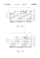
- FIGS. 1(a)-(f) is a schematic diagram showing a preferred embodiment of a contact plug manufacturing process according to the present invention
- FIGS. 2(a)-(f) is a schematic diagram showing another preferred embodiment of a contact plug manufacturing process according to the present invention.
- FIGS. 3(a)-(g) is a schematic diagram showing a third preferred embodiment of a contact plug manufacturing process according to the present inventing.
- FIGS. 4(a)-(g) is a schematic diagram showing a fourth preferred embodiment of a contact plug manufacturing process according to the present invention.
- CVD chemical vapor deposition
- the dielectric layers 1O, 2O, and 3O are selected among a silicon dioxide (SiO 2 ) layer, a phosphosilicate glass (PSG) layer, a borophosphosilicate glass (BPSG) layer, a thermal oxide layer, and a non-doped silicate glass (NSG) layer.
- the conducting layers 1P, 2P, 3P, and 4P are polysilicon layers. There are two regions on the wafer. They are device area D and edge area E respectively. The present invention brings the edge area E into focus.
- FIGS. 1(b) and 1(c) indicate the forming of a fourth dielectric layer 4O and a photoresist layer R on both areas D and E.
- FIG. 1(d) shows the next steps.
- a photolithography and etching procedure such as dry etching is executed to etch the fourth dielectric layer 4O to form a contact hole C on device area D.
- the key point is to leave the fourth dielectric layer 4O on edge area E.
- FIGS. 1(e) and 1(f) indicate the removing of the remaining photoresist layer on both areas D and E. Then magnetron DC sputtering and blanket tungsten deposition method are executed to form a metal film M and a tungsten film W on both areas D and E.
- This metal film M is selected as titanic or titanic/titanium nitride (Ti/TiN) film.
- Ti/TiN titanic or titanic/titanium nitride
- this titanium nitride film is formed by rapid thermal nitridation (RTN) or reactive sputtering deposition procedure. At last, execute a etchback procedure to form a contact plug in the contact hole C.
- the difference between conventional technique and present invention is to make metal film M break contact with the third conducting layer 3P on edge area E.
- Titanic film will react with the third conducting layer 3P to form titanium silicide (TiSi 2 ) film, and titanium silicide has much different thermal expansion coefficient from dielectric materials.
- titanium silicide film and titanic film peel off dielectric layer on edge area E. Introducing the fourth dielectric layer 40 solves this problem properly.
- FIGS. 2(a) and 2(b) show a chemical vapor deposition method used to form dielectric layers 1O, 2O, 3O, and 4O and conducting layers 1P, 2P, 3P, and 4P on substrate S.
- FIG. 2(c) shows the forming of a photoresist layer R on both areas D and E and the stripping of the photoresist layer R on edge area E.
- FIG. 2(d) illustrates the following steps. Executing a photolithography and etching procedure such as dry etching to etch the fourth dielectric layer 4O to form a contact hole C on device area D. An etcher with clamps is used to keep the fourth dielectric layer 4O on edge area E.
- a photolithography and etching procedure such as dry etching to etch the fourth dielectric layer 4O to form a contact hole C on device area D.
- An etcher with clamps is used to keep the fourth dielectric layer 4O on edge area E.
- FIGS. 2(e) and 2(f) indicates the methods including magnetron DC sputtering, blanket tungsten deposition, and etchback to form a tungsten plug.
- This example has the same effect as example 1.
- Metal film M has no contact with the third conducting layer 3P due to the introduction of the fourth dielectric layer 4O.
- the generation of titanium silicide layer is impossible in this case. Peeling on edge area E due to the generation of titanium silicide layer does not occur even during thermal treat process.
- FIGS. 3(a)-3(c) show the forming of dielectric layers 1O, 2O, 3O, and 4O, conducting layers 1P, 2P, 3P, and 4P, and photoresist layer R on substrate S, and the removing of the photoresist layer R on edge area E.
- FIG. 3(d) Shown in FIG. 3(d) is a photolithography and etching procedure such as dry etching executed to form a contact C on device area D and to remove the fourth dielectric layer 4O entirely on edge area E. An etcher without clamps is used in this case.
- FIG. 3(e) shows that a dry etching by means of a plasma etching technique using ozone (O 3 ) is executed to remove the photoresist layer R remained on the fourth dielectric layer 4O and the third conducting layer 3P on edge area.
- FIGS. 3(f) and 3(g) indicate the methods including magnetron DC sputtering, blanket tungsten deposition, and etchback to form a tungsten plug.
- the difference between conventional technique and this sample is to make metal film M break contact with the third conducting layer 3P on edge area E. Titanic film will react with the third conducting layer 3P to form titanium silicide film, and titanium silicide has much different thermal expansion coefficient from dielectric materials. During thermal treat process, titanium silicide film and titanic film peel off dielectric layer on edge area E. Removing the third conducting layer 3P solves this problem properly.
- FIG. 4(a) shows a chemical vapor deposition method executed to form dielectric layers 1O, 2O, and 3O and conducting layers 1P, 2P, 3P, and 4P on substrate S.
- FIG. 4(b) Shown in FIG. 4(b) is a dry etching procedure executed to remove the third conducting layer 3P on edge area E, and in FIG. 4(c) is the chemical vapor deposition executed to form the fourth dielectric layer 4O on both areas D and E.
- FIG. 4(d) shows the steps of forming a photoresist layer R over the fourth dielectric 4O, and stripping the photoresist layer R over the fourth dielectric 4O on edge area E.
- FIG. 4(e) indicates that a photolithography and etching procedure such as dry etching is executed to form a contact hole C on device area D and to remove the fourth dielectric layer 4O entirely on edge area E. An etcher without clamps is used in this case.
- FIGS. 4(f) and 4(g) indicate the methods including magnetron DC sputtering, blanket tungsten deposition, and etchback to form a tungsten plug.
- This example has the same effect as example 3.
- the metal film M has no contact with the third conducting layer 3P due to the removing of the third conducting layer 3P on edge area E.
- the generation of titanium silicide layer is impossible in this case. Peeling on edge area E due to the generation of titanium silicide layer does not occur even during thermal treat process.
Landscapes
- Internal Circuitry In Semiconductor Integrated Circuit Devices (AREA)
Abstract
Description
Claims (23)
Applications Claiming Priority (2)
| Application Number | Priority Date | Filing Date | Title |
|---|---|---|---|
| TW085115719A TW317651B (en) | 1996-12-19 | 1996-12-19 | Method of preventing wafer edge region from generating peeling phenomena |
| TW85115719 | 1996-12-19 |
Publications (1)
| Publication Number | Publication Date |
|---|---|
| US5930593A true US5930593A (en) | 1999-07-27 |
Family
ID=21625624
Family Applications (1)
| Application Number | Title | Priority Date | Filing Date |
|---|---|---|---|
| US08/895,430 Expired - Lifetime US5930593A (en) | 1996-12-19 | 1997-07-16 | Method for formating device on wafer without peeling |
Country Status (2)
| Country | Link |
|---|---|
| US (1) | US5930593A (en) |
| TW (1) | TW317651B (en) |
Families Citing this family (1)
| Publication number | Priority date | Publication date | Assignee | Title |
|---|---|---|---|---|
| TW201043856A (en) | 2009-06-12 | 2010-12-16 | Sheng-Yi Zhuang | Method for manufacturing light cover |
Citations (10)
| Publication number | Priority date | Publication date | Assignee | Title |
|---|---|---|---|---|
| US4188258A (en) * | 1978-05-18 | 1980-02-12 | Gulton Industries, Inc. | Process for fabricating strain gage transducer |
| US5164338A (en) * | 1988-04-28 | 1992-11-17 | U.S. Philips Corporation | Method of manufacturing a polycrystalline semiconductor resistance layer of silicon on a silicon body and silicon pressure sensor having such a resistance layer |
| US5472916A (en) * | 1993-04-05 | 1995-12-05 | Siemens Aktiengesellschaft | Method for manufacturing tunnel-effect sensors |
| US5520785A (en) * | 1994-01-04 | 1996-05-28 | Motorola, Inc. | Method for enhancing aluminum nitride |
| US5571746A (en) * | 1995-10-19 | 1996-11-05 | Chartered Semiconductor Manufacturing Pte Ltd. | Method of forming a back end capacitor with high unit capacitance |
| US5616523A (en) * | 1993-05-06 | 1997-04-01 | Robert Bosch Gmbh | Method of manufacturing sensor |
| US5618380A (en) * | 1995-12-18 | 1997-04-08 | Vlsi Technology, Inc. | Wafer edge sealing |
| US5620931A (en) * | 1990-08-17 | 1997-04-15 | Analog Devices, Inc. | Methods for fabricating monolithic device containing circuitry and suspended microstructure |
| US5620929A (en) * | 1994-02-23 | 1997-04-15 | Honda Giken Kogyo Kabushiki Kaisha | Method of manufacturing a gas flow type sensor |
| US5783482A (en) * | 1997-09-12 | 1998-07-21 | Taiwan Semiconductor Manufacturing Company, Ltd. | Method to prevent oxide peeling induced by sog etchback on the wafer edge |
-
1996
- 1996-12-19 TW TW085115719A patent/TW317651B/en active
-
1997
- 1997-07-16 US US08/895,430 patent/US5930593A/en not_active Expired - Lifetime
Patent Citations (10)
| Publication number | Priority date | Publication date | Assignee | Title |
|---|---|---|---|---|
| US4188258A (en) * | 1978-05-18 | 1980-02-12 | Gulton Industries, Inc. | Process for fabricating strain gage transducer |
| US5164338A (en) * | 1988-04-28 | 1992-11-17 | U.S. Philips Corporation | Method of manufacturing a polycrystalline semiconductor resistance layer of silicon on a silicon body and silicon pressure sensor having such a resistance layer |
| US5620931A (en) * | 1990-08-17 | 1997-04-15 | Analog Devices, Inc. | Methods for fabricating monolithic device containing circuitry and suspended microstructure |
| US5472916A (en) * | 1993-04-05 | 1995-12-05 | Siemens Aktiengesellschaft | Method for manufacturing tunnel-effect sensors |
| US5616523A (en) * | 1993-05-06 | 1997-04-01 | Robert Bosch Gmbh | Method of manufacturing sensor |
| US5520785A (en) * | 1994-01-04 | 1996-05-28 | Motorola, Inc. | Method for enhancing aluminum nitride |
| US5620929A (en) * | 1994-02-23 | 1997-04-15 | Honda Giken Kogyo Kabushiki Kaisha | Method of manufacturing a gas flow type sensor |
| US5571746A (en) * | 1995-10-19 | 1996-11-05 | Chartered Semiconductor Manufacturing Pte Ltd. | Method of forming a back end capacitor with high unit capacitance |
| US5618380A (en) * | 1995-12-18 | 1997-04-08 | Vlsi Technology, Inc. | Wafer edge sealing |
| US5783482A (en) * | 1997-09-12 | 1998-07-21 | Taiwan Semiconductor Manufacturing Company, Ltd. | Method to prevent oxide peeling induced by sog etchback on the wafer edge |
Also Published As
| Publication number | Publication date |
|---|---|
| TW317651B (en) | 1997-10-11 |
Similar Documents
| Publication | Publication Date | Title |
|---|---|---|
| US7157351B2 (en) | Ozone vapor clean method | |
| US5948702A (en) | Selective removal of TixNy | |
| US5346586A (en) | Method for selectively etching polysilicon to gate oxide using an insitu ozone photoresist strip | |
| US6165881A (en) | Method of forming salicide poly gate with thin gate oxide and ultra narrow gate width | |
| US20050106888A1 (en) | Method of in-situ damage removal - post O2 dry process | |
| US4808259A (en) | Plasma etching process for MOS circuit pregate etching utiliizing a multi-step power reduction recipe | |
| US5792672A (en) | Photoresist strip method | |
| US6221772B1 (en) | Method of cleaning the polymer from within holes on a semiconductor wafer | |
| US5872063A (en) | Self-aligned contact structures using high selectivity etching | |
| JPH1168095A (en) | Method for manufacturing semiconductor device | |
| US6054377A (en) | Method for forming an inlaid via in a semiconductor device | |
| US6136691A (en) | In situ plasma clean for tungsten etching back | |
| US6860275B2 (en) | Post etching treatment process for high density oxide etcher | |
| US6554004B1 (en) | Method for removing etch residue resulting from a process for forming a via | |
| JP2001060672A (en) | Etching method and etching mask | |
| US6239006B1 (en) | Native oxide removal with fluorinated chemistry before cobalt silicide formation | |
| US6043206A (en) | Solutions for cleaning integrated circuit substrates | |
| KR100299386B1 (en) | Gate electrode formation method of semiconductor device | |
| EP0731501A1 (en) | Method for plasma etching an oxide/polycide structure | |
| US5930593A (en) | Method for formating device on wafer without peeling | |
| EP0967640A2 (en) | Method of making a self-aligned contact | |
| JPH11121621A (en) | Method for forming self-aligned contact hole | |
| WO2005048342A1 (en) | Method for preventing an increase in contact hole width during contact formation | |
| US6071353A (en) | Protection of consumable susceptor during etch by a second coating of another consumable material | |
| JPH11354503A (en) | Etching apparatus, operating method thereof, and method of manufacturing semiconductor device |
Legal Events
| Date | Code | Title | Description |
|---|---|---|---|
| AS | Assignment |
Owner name: MOSEL VITELIC INC., TAIWAN Free format text: ASSIGNMENT OF ASSIGNORS INTEREST;ASSIGNORS:TSAI, CHENG-HAUN;HUANG, YUI-PING;TSENG, MAO-SONG;AND OTHERS;REEL/FRAME:008648/0479 Effective date: 19970530 |
|
| STCF | Information on status: patent grant |
Free format text: PATENTED CASE |
|
| FEPP | Fee payment procedure |
Free format text: PAYOR NUMBER ASSIGNED (ORIGINAL EVENT CODE: ASPN); ENTITY STATUS OF PATENT OWNER: LARGE ENTITY Free format text: PAYER NUMBER DE-ASSIGNED (ORIGINAL EVENT CODE: RMPN); ENTITY STATUS OF PATENT OWNER: LARGE ENTITY |
|
| FPAY | Fee payment |
Year of fee payment: 4 |
|
| AS | Assignment |
Owner name: PROMOS TECHNOLOGIES INC., TAIWAN Free format text: ASSIGNMENT OF ASSIGNORS INTEREST;ASSIGNOR:MOSEL VITELIC, INC.;REEL/FRAME:015334/0772 Effective date: 20040427 |
|
| FPAY | Fee payment |
Year of fee payment: 8 |
|
| REMI | Maintenance fee reminder mailed | ||
| FPAY | Fee payment |
Year of fee payment: 12 |
|
| SULP | Surcharge for late payment |
Year of fee payment: 11 |