US5922988A - Thermoelectric material - Google Patents
Thermoelectric material Download PDFInfo
- Publication number
- US5922988A US5922988A US08/895,378 US89537897A US5922988A US 5922988 A US5922988 A US 5922988A US 89537897 A US89537897 A US 89537897A US 5922988 A US5922988 A US 5922988A
- Authority
- US
- United States
- Prior art keywords
- barrier layer
- semiconductor
- interface
- conductive layer
- barrier
- Prior art date
- Legal status (The legal status is an assumption and is not a legal conclusion. Google has not performed a legal analysis and makes no representation as to the accuracy of the status listed.)
- Expired - Fee Related
Links
- 239000000463 material Substances 0.000 title claims abstract description 38
- 230000004888 barrier function Effects 0.000 claims abstract description 100
- 239000004065 semiconductor Substances 0.000 claims abstract description 50
- 229910005331 FeSi2 Inorganic materials 0.000 claims description 6
- 229910002665 PbTe Inorganic materials 0.000 claims description 6
- OCGWQDWYSQAFTO-UHFFFAOYSA-N tellanylidenelead Chemical compound [Pb]=[Te] OCGWQDWYSQAFTO-UHFFFAOYSA-N 0.000 claims description 6
- 229910000577 Silicon-germanium Inorganic materials 0.000 claims description 5
- 230000000052 comparative effect Effects 0.000 description 14
- 239000013078 crystal Substances 0.000 description 14
- 238000004544 sputter deposition Methods 0.000 description 13
- 238000000034 method Methods 0.000 description 11
- XKRFYHLGVUSROY-UHFFFAOYSA-N Argon Chemical compound [Ar] XKRFYHLGVUSROY-UHFFFAOYSA-N 0.000 description 10
- 239000000758 substrate Substances 0.000 description 10
- 238000001000 micrograph Methods 0.000 description 9
- 235000019592 roughness Nutrition 0.000 description 8
- 238000012360 testing method Methods 0.000 description 6
- 229910052786 argon Inorganic materials 0.000 description 5
- 239000007789 gas Substances 0.000 description 5
- 239000000203 mixture Substances 0.000 description 5
- 238000013139 quantization Methods 0.000 description 5
- 230000005283 ground state Effects 0.000 description 4
- 230000003746 surface roughness Effects 0.000 description 4
- 230000008646 thermal stress Effects 0.000 description 4
- 230000007423 decrease Effects 0.000 description 3
- 238000006073 displacement reaction Methods 0.000 description 2
- 239000011521 glass Substances 0.000 description 2
- 230000007935 neutral effect Effects 0.000 description 2
- 238000005381 potential energy Methods 0.000 description 2
- 238000004886 process control Methods 0.000 description 2
- 239000010409 thin film Substances 0.000 description 2
- 229910005900 GeTe Inorganic materials 0.000 description 1
- XUIMIQQOPSSXEZ-UHFFFAOYSA-N Silicon Chemical compound [Si] XUIMIQQOPSSXEZ-UHFFFAOYSA-N 0.000 description 1
- 239000000969 carrier Substances 0.000 description 1
- 239000000919 ceramic Substances 0.000 description 1
- 238000007796 conventional method Methods 0.000 description 1
- 230000002950 deficient Effects 0.000 description 1
- 238000010586 diagram Methods 0.000 description 1
- 238000009792 diffusion process Methods 0.000 description 1
- 238000007599 discharging Methods 0.000 description 1
- 230000002349 favourable effect Effects 0.000 description 1
- RQQRAHKHDFPBMC-UHFFFAOYSA-L lead(ii) iodide Chemical compound I[Pb]I RQQRAHKHDFPBMC-UHFFFAOYSA-L 0.000 description 1
- 238000004519 manufacturing process Methods 0.000 description 1
- 238000012986 modification Methods 0.000 description 1
- 230000004048 modification Effects 0.000 description 1
- 239000002120 nanofilm Substances 0.000 description 1
- 229910052710 silicon Inorganic materials 0.000 description 1
- 239000010703 silicon Substances 0.000 description 1
- 230000007480 spreading Effects 0.000 description 1
Images


Classifications
-
- H—ELECTRICITY
- H10—SEMICONDUCTOR DEVICES; ELECTRIC SOLID-STATE DEVICES NOT OTHERWISE PROVIDED FOR
- H10N—ELECTRIC SOLID-STATE DEVICES NOT OTHERWISE PROVIDED FOR
- H10N10/00—Thermoelectric devices comprising a junction of dissimilar materials, i.e. devices exhibiting Seebeck or Peltier effects
- H10N10/80—Constructional details
- H10N10/85—Thermoelectric active materials
- H10N10/851—Thermoelectric active materials comprising inorganic compositions
- H10N10/852—Thermoelectric active materials comprising inorganic compositions comprising tellurium, selenium or sulfur
-
- H—ELECTRICITY
- H10—SEMICONDUCTOR DEVICES; ELECTRIC SOLID-STATE DEVICES NOT OTHERWISE PROVIDED FOR
- H10N—ELECTRIC SOLID-STATE DEVICES NOT OTHERWISE PROVIDED FOR
- H10N10/00—Thermoelectric devices comprising a junction of dissimilar materials, i.e. devices exhibiting Seebeck or Peltier effects
- H10N10/80—Constructional details
- H10N10/85—Thermoelectric active materials
- H10N10/851—Thermoelectric active materials comprising inorganic compositions
- H10N10/8556—Thermoelectric active materials comprising inorganic compositions comprising compounds containing germanium or silicon
Definitions
- the present invention relates to thermoelectric materials.
- thermoelectric materials of the type in which a heterojunction interface between a conductive layer and a barrier layer is formed into a flat atomic surface (see, for example, U.S. Pat. No. 5,436,467).
- thermoelectric material In the thermoelectric material, the energy gap in the barrier layer is maintained to be much wider than the energy gap in the conductive layer to create a large difference between the two energy gaps, whereby quantum wells are formed in the conductive layers. As a result, the electric conductivity of the thermoelectric material is heightened, and an improved thermoelectric performance is exhibited.
- the layers have heretofore been formed by the molecular beam epitaxial method (MBE), atomic epitaxial layer method (ALE) or the like method.
- MBE molecular beam epitaxial method
- ALE atomic epitaxial layer method
- thermoelectric material of this type there is a difference in the coefficient of thermal expansion between the barrier layer and the conductive layer, due to the difference in the crystalline structures of the semiconductors and the difference in the lattice constants. Therefore, when the heterojunction interface between the barrier layer and the conductive layer is formed into a flat atomic surface and then the temperature is elevated in order to maximize the thermoelectric performance of the thermoelectric material to its limit, a relatively large thermal stress is produced in the heterojunction interface. As a result, cracks are produced in the conductive layer and/or in the barrier layer due to the thermal stress, thereby breaking the thermoelectric material.
- thermoelectric materials are produced.
- thermoelectric material which has an excellent thermoelectric performance even when it is used at elevated temperatures, and which increases the productivity and lowers the cost of production.
- present invention fulfills these needs, and provides further related advantages.
- thermoelectric material which has an excellent thermoelectric performance even when used at elevated temperatures, and which is efficient and cost effective to produce.
- a thermoelectric material is provided, having conductive layers and barrier layers that are alternatingly formed one upon the other.
- the conductive layers are made of a first semiconductor only, and the barrier layers are made of a second semiconductor only, that is different from the first semiconductor.
- the interface of the barrier layer relative to the conductive layer is roughly formed to include a plurality of protuberances and a plurality of recesses, the interface of the conductive layer relative to the barrier layer is roughly formed to fit the interface of the barrier layer, and the ratio Ry/t is ⁇ 0.1, where Ry is the maximum height of the protuberance on the barrier layer and t is the thickness of the barrier layer.
- thermoelectric material are formed by sputtering which is a generally employed method of forming thin films.
- the surface (interface) of the barrier layer is rough, including a plurality of recesses and protuberances formed by sputtering.
- the thermoelectric material overcomes a relatively large thermal stress that generates near the heterojunction interface, and exhibits an excellent thermoelectric performance without being broken.
- thermoelectric material is efficiently produced at a low cost.
- FIG. 1 is a diagram illustrating a thermoelectric material provided in accordance with a preferred embodiment of the present invention.
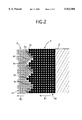
- FIG. 2 is an explanatory view showing a first example of a step of forming the layers of the material of FIG. 1.
- FIG. 3 is a microphotograph of a first example of an interface of a very thin film-like barrier layer.
- FIG. 4 is a microphotograph of a second example of an interface of a very thin film-like barrier layer.
- FIG. 5 is a microphotograph of a third example of an interface of a very thin film-like barrier layer.
- FIG. 6 is a microphotograph showing the roughness of the interface of the first example of the very thin film-like barrier layer illustrated in FIG. 3.
- FIG. 7 is a microphotograph showing the roughness of the interface of the second example of the very thin film-like barrier layer illustrated in FIG. 4.
- FIG. 8 is a microphotograph showing the roughness of the interface of the third example of the very thin film-like barrier layer illustrated in FIG. 5.
- FIG. 9 is an explanatory view showing a second example of a step of forming layers in a thermoelectric material.
- FIG. 10 is an explanatory view showing a third example of a step of forming layers in a thermoelectric material.
- FIG. 11 is an explanatory view showing a fourth example of a step of forming layers in a thermoelectric material.
- thermoelectric material 1 is formed in accordance with a preferred embodiment of the present invention on a substrate 2, having very thin film-like conductive layers 3 alternatingly formed with very thin film-like barrier layers 4.
- the conductive layers 3 are made of a first semiconductor s 1 only, and the barrier layers are made of a second semiconductor s 2 only, that is different from the first semiconductor s 1 .
- the interface of the barrier layer 4 relative to the conductive layer 3 is roughly formed to include a plurality of protuberances a 1 and recesses b 1 .
- the interface of the conductive layer 3 relative to the barrier layer 4 is roughly formed to fit the interface of the barrier layer 4, i.e., to include a plurality of recesses b 2 receiving the protuberances a 1 of the barrier layer 4 and a plurality of protuberances a 2 received by the recesses b 1 of the barrier layer 4.
- the ratio Ry/t of the maximum height Ry of the protuberance a 1 at the interface of the barrier layer 4 to the thickness t of the barrier layer 4 is set to be Ry/t ⁇ 0. 1.
- the layers of the thermoelectric material 1 are formed by sputtering which is a generally employed method of forming thin layers.
- the barrier layer 4 made of the second semiconductor s 2 is formed on the substrate 2 by sputtering, a plurality of protuberances a 1 made of the second semiconductor s 2 are formed on the surface of the barrier layer 4 and a plurality of recesses b 1 where no second semiconductor s 2 exists are formed in the surface of the barrier layer 4, due to uneven growth of crystals and surface diffusion in the initial stage of forming the barrier layer 4.
- the protuberances a 1 are covered with the first semiconductor s 1 to form recesses b 2 and the recesses b 1 are filled with the first semiconductor s 1 to form protuberances a 2 . Therefore, a plurality of protuberances a 2 made of the first semiconductor s 1 are formed on the surface of the conductive layer 3 and a plurality of recesses b 2 where no first semiconductor s 1 exists are formed in the surface of the conductive layer 3.
- the crystals in the conductive layer 3 tend to grow in the crystal orientation B 2 which is the same as the crystal orientation B 1 of the barrier layer 4.
- an atom A 1 on the barrier layer 4 side tends to overlap with an atom A 2 on the conductive layer 3 side as shown by the lined circles.
- the two atoms A 1 and A 2 move to neutral positions where they do not overlap with each other, and other surrounding atoms undergo displacement, too.
- strain of the order of atoms occurs in the crystalline structure at the heterojunction interface between the barrier layer 4 and the conductive layer 3, and atoms are restricted at the heterojunction interface. That is, even when an external force acts on the heterojunction interface between the barrier layer 4 and the conductive layer 3, the atoms hardly move at the heterojunction interface. This means that the interfacial strength is enhanced between the barrier layer 4 and the conductive layer 3.
- the ratio Ry/t of the maximum height Ry of the protuberance a 1 of the barrier layer 4 to the thickness t of the barrier layer 4 is set to be Ry/t ⁇ 0.1, it is possible to increase the strain and to sufficiently enhance the interfacial strength.
- the interface of the barrier layer 4 relative to the conductive layer 3 is roughly formed to include a plurality of protuberances a 1 and a plurality of recesses b 1 in the same manner as described above. It is therefore considered that the same phenomenon as the one mentioned above takes place between the conductive layer 3 and the barrier layer 4.
- the step of forming the layer is repeated and, lastly, the barrier layer 4 made of the second semiconductor s 2 is formed.
- thermoelectric material 1 provided in accordance with the present invention overcomes a relatively large thermal stress that generates at the heterojunction interface, and exhibits an excellent thermoelectric performance.
- thermoelectric material provided in accordance with the present invention, it is possible to expand the temperature range toward the higher temperature side in order to broaden an optimum range of temperatures at which the thermoelectric material is used.
- thermoelectric material exhibits enhanced thermoelectric performance on account of the reasons described below.
- the heat conduction of the semiconductor depends chiefly upon the lattice vibration.
- the lattice vibration receives interference of the interface, and the heat conductivity decreases.
- the contact area of the interface can be increased to become larger than that of a flat interface, whereby interference of the interface with the lattice vibration is enhanced to further decrease the heat conductivity.
- the performance index which is one of the factors expressing thermoelectric performance varies in reverse proportion to the heat conductivity.
- Examples of the first semiconductor s 1 of which the conductive layer 3 is made include p-type semiconductors such as Fe 0 .9 Mn 0 .1 Si 2 FeSi 2 semiconductor!, (Si 0 .8 Ge 0 .2)B 0 .003 SiGe semiconductor!, (PbTe 0 .95 Se 0 .05)Na 0 .01 PbTe semiconductor!, and (GeTe) 0 .85 (AgSbTe 2 ) 0 .15 PbTe substituted semiconductor!, n-type semiconductors such as Fe 0 .9 Co 0 .1 Si 2 FeSi 2 semiconductor!, (Si 0 .8 Ge 0 .2) P 0 .002 SiGe semiconductor!, (Pb 0 .95 Ge 0 .05 Te) (PbI 2 ) 0 .001 PbTe semiconductor!, and p-type and n-type BiTe semiconductors.
- Examples of the second semiconductor s 2 of which the layer 4 is made include Si, FeSi 2 FeSi 2 semiconductor!, Si 0 .8 Ge 0 .2 SiGe semiconductor! and (Pb 0 .9 Eu 0 .07)Te PbTe semiconductor!.
- the inside of the chamber is evacuated to about 10 -3 Torr and is replaced with an argon gas.
- the electric discharge is started.
- the flow rate of argon gas is set at 5 to 25 SCCM (SCCM: mass flow rate)
- the electric power for sputtering is set at 50 to 500 watts
- the sputtering rate is set at 10 to 300 ⁇ /second.
- the conductive layers 3 and the barrier layers 4 are controlled to have predetermined thicknesses according to the sputtering rate and the sputtering time.
- Table 1 shows the conditions under which a thermoelectric material 1 is produced, and under which Examples 1 and 2 were conducted while changing the thickness of the barrier layer 4.
- Table 2 shows the roughness at the interfaces of the barrier layers 4, the thicknesses t of the barrier layers 4 and of the conductive layers 3, and the ratio Ry/t of the maximum height Ry of the protuberance a 1 of the barrier layer 4 to the thickness t of the barrier layer 4 in Examples 1 and 2 and in the Comparative Example.
- FIGS. 6, 7 and 8 are microphotographs showing the roughnesses at the interfaces of the fiftieth barrier layers 4 of Examples 1, 2 and Comparative Example, obtained by using an atomic force microscope (AFM).
- the surface roughnesses of Examples 1, 2 and the Comparative Example were calculated by measuring the roughnesses at the interfaces of the barrier layers over an area of about 1 ⁇ m long and about 1 ⁇ m wide, using an atomic force microscope, and making reference to JIS B0601 (1994) which specifies the surface roughness.
- thermoelectric outputs and the electric conductivities were measured by the same methods as those mentioned above.
- Examples 1 and 2 exhibit favorable heat resistances and excellent thermoelectric performances, even at high temperatures.
- thermoelectric material which exhibits an excellent thermoelectric performance even when it is used at high temperatures, and that can be produced at a low cost, has been shown and described.
Landscapes
- Chemical & Material Sciences (AREA)
- Inorganic Chemistry (AREA)
- Physical Deposition Of Substances That Are Components Of Semiconductor Devices (AREA)
Abstract
A thermoelectric material which exhibits an excellent thermoelectric performance even when it is used at elevated temperatures is shown and described. A thermoelectric material is provided having conductive layers made of a first semiconductor only, and barrier layers made of a second semiconductor only, that are alternatingly formed one upon the other. The interface of the barrier layer relative to the conductive layer is roughly formed to include a plurality of protuberances and a plurality of recesses, and the interface of the conductive layer relative to the barrier layer is roughly formed to fit the interface of the barrier layer. The ratio Ry/t of the maximum height Ry of the protuberance on the barrier layer to the thickness t of the barrier layer is set to be Ry/t≧0.1. This makes it possible to enhance the strength of the heterojunction interface between the barrier layer and the conductive layer and to improve the heat resistance.
Description
The present invention relates to thermoelectric materials.
There has heretofore been known thermoelectric materials of the type in which a heterojunction interface between a conductive layer and a barrier layer is formed into a flat atomic surface (see, for example, U.S. Pat. No. 5,436,467).
In the thermoelectric material, the energy gap in the barrier layer is maintained to be much wider than the energy gap in the conductive layer to create a large difference between the two energy gaps, whereby quantum wells are formed in the conductive layers. As a result, the electric conductivity of the thermoelectric material is heightened, and an improved thermoelectric performance is exhibited.
In order to strictly control the interfaces of the barrier layer and the conductive layer, therefore, the layers have heretofore been formed by the molecular beam epitaxial method (MBE), atomic epitaxial layer method (ALE) or the like method.
In a thermoelectric material of this type, however, there is a difference in the coefficient of thermal expansion between the barrier layer and the conductive layer, due to the difference in the crystalline structures of the semiconductors and the difference in the lattice constants. Therefore, when the heterojunction interface between the barrier layer and the conductive layer is formed into a flat atomic surface and then the temperature is elevated in order to maximize the thermoelectric performance of the thermoelectric material to its limit, a relatively large thermal stress is produced in the heterojunction interface. As a result, cracks are produced in the conductive layer and/or in the barrier layer due to the thermal stress, thereby breaking the thermoelectric material.
Furthermore, in order to form layers via the above-mentioned methods, very expensive equipment and very complex process control are required. In addition, despite the process control, the occurrence of defective products is high, resulting in an increase in the cost at which the thermoelectric materials are produced.
A need therefore exists for a thermoelectric material which has an excellent thermoelectric performance even when it is used at elevated temperatures, and which increases the productivity and lowers the cost of production. The present invention fulfills these needs, and provides further related advantages.
Briefly, the present invention provides a thermoelectric material which has an excellent thermoelectric performance even when used at elevated temperatures, and which is efficient and cost effective to produce. In a preferred embodiment, a thermoelectric material is provided, having conductive layers and barrier layers that are alternatingly formed one upon the other. The conductive layers are made of a first semiconductor only, and the barrier layers are made of a second semiconductor only, that is different from the first semiconductor. The interface of the barrier layer relative to the conductive layer is roughly formed to include a plurality of protuberances and a plurality of recesses, the interface of the conductive layer relative to the barrier layer is roughly formed to fit the interface of the barrier layer, and the ratio Ry/t is ≧0.1, where Ry is the maximum height of the protuberance on the barrier layer and t is the thickness of the barrier layer.
The layers of the thermoelectric material are formed by sputtering which is a generally employed method of forming thin films. The surface (interface) of the barrier layer is rough, including a plurality of recesses and protuberances formed by sputtering.
When a heterojunction interface is created by forming a conductive layer on the barrier layer, it is believed that the below-mentioned phenomenon occurs.
That is, crystals in the conductive layer tend to grow in such a way that the orientation of crystals in the conductive layer agrees with that in the barrier layer. In the recesses and protuberances, therefore, an atom of the barrier layer tends to overlap with an atom of the conductive layer. In fact, however, it is impossible for two atoms to exist, overlapping with each other. Therefore, the atoms move to neutral positions where they do not overlap with each other, and other surrounding atoms undergo displacement, too. Thus, strain of the order of atoms occurs in the crystalline structure at the heterojunction interface between the barrier layer and the conductive layer, and atoms are restricted at the heterojunction interface. That is, even when an external force acts on the heterojunction interface between the barrier layer and the conductive layer, atoms hardly move at the heterojunction interface. This means that the interfacial strength is enhanced between the barrier layer and the conductive layer.
Therefore, if the ratio Ry/t of the maximum height Ry of the protuberances of the barrier layer to the thickness t of the barrier layer is set to be Ry/t≧0.1, it is possible to increase the strain and to sufficiently enhance the interfacial strength. Accordingly, even when used at high temperatures, the thermoelectric material overcomes a relatively large thermal stress that generates near the heterojunction interface, and exhibits an excellent thermoelectric performance without being broken.
Moreover, since the layers are formed by a generally employed method of forming thin films, the thermoelectric material is efficiently produced at a low cost.
FIG. 1 is a diagram illustrating a thermoelectric material provided in accordance with a preferred embodiment of the present invention.
FIG. 2 is an explanatory view showing a first example of a step of forming the layers of the material of FIG. 1.
FIG. 3 is a microphotograph of a first example of an interface of a very thin film-like barrier layer.
FIG. 4 is a microphotograph of a second example of an interface of a very thin film-like barrier layer.
FIG. 5 is a microphotograph of a third example of an interface of a very thin film-like barrier layer.
FIG. 6 is a microphotograph showing the roughness of the interface of the first example of the very thin film-like barrier layer illustrated in FIG. 3.
FIG. 7 is a microphotograph showing the roughness of the interface of the second example of the very thin film-like barrier layer illustrated in FIG. 4.
FIG. 8 is a microphotograph showing the roughness of the interface of the third example of the very thin film-like barrier layer illustrated in FIG. 5.
FIG. 9 is an explanatory view showing a second example of a step of forming layers in a thermoelectric material.
FIG. 10 is an explanatory view showing a third example of a step of forming layers in a thermoelectric material.
FIG. 11 is an explanatory view showing a fourth example of a step of forming layers in a thermoelectric material.
As illustrated in FIG. 1, a thermoelectric material 1 is formed in accordance with a preferred embodiment of the present invention on a substrate 2, having very thin film-like conductive layers 3 alternatingly formed with very thin film-like barrier layers 4. The conductive layers 3 are made of a first semiconductor s1 only, and the barrier layers are made of a second semiconductor s2 only, that is different from the first semiconductor s1.
The interface of the barrier layer 4 relative to the conductive layer 3 is roughly formed to include a plurality of protuberances a1 and recesses b1. The interface of the conductive layer 3 relative to the barrier layer 4 is roughly formed to fit the interface of the barrier layer 4, i.e., to include a plurality of recesses b2 receiving the protuberances a1 of the barrier layer 4 and a plurality of protuberances a2 received by the recesses b1 of the barrier layer 4.
The ratio Ry/t of the maximum height Ry of the protuberance a1 at the interface of the barrier layer 4 to the thickness t of the barrier layer 4 is set to be Ry/t≧0. 1.
In a preferred embodiment, the layers of the thermoelectric material 1 are formed by sputtering which is a generally employed method of forming thin layers.
When the barrier layer 4 made of the second semiconductor s2 is formed on the substrate 2 by sputtering, a plurality of protuberances a1 made of the second semiconductor s2 are formed on the surface of the barrier layer 4 and a plurality of recesses b1 where no second semiconductor s2 exists are formed in the surface of the barrier layer 4, due to uneven growth of crystals and surface diffusion in the initial stage of forming the barrier layer 4.
Next, when the conductive layer 3 made of the first semiconductor s1 is formed on the surface of the barrier layer 4, the protuberances a1 are covered with the first semiconductor s1 to form recesses b2 and the recesses b1 are filled with the first semiconductor s1 to form protuberances a2. Therefore, a plurality of protuberances a2 made of the first semiconductor s1 are formed on the surface of the conductive layer 3 and a plurality of recesses b2 where no first semiconductor s1 exists are formed in the surface of the conductive layer 3.
It is believed that the below-mentioned phenomenon takes place when the heterojunction interface is created by forming the conducting layer 3 on the barrier layer 4.
That is, as illustrated in FIG. 2, the crystals in the conductive layer 3 tend to grow in the crystal orientation B2 which is the same as the crystal orientation B1 of the barrier layer 4. In the recesses and protuberances b1, b2, a1, and a2 shown in FIG. 2, therefore, an atom A1 on the barrier layer 4 side tends to overlap with an atom A2 on the conductive layer 3 side as shown by the lined circles. Actually, however, it is impossible for the atoms to overlap with each other. Therefore, the two atoms A1 and A2 move to neutral positions where they do not overlap with each other, and other surrounding atoms undergo displacement, too. Thus, strain of the order of atoms occurs in the crystalline structure at the heterojunction interface between the barrier layer 4 and the conductive layer 3, and atoms are restricted at the heterojunction interface. That is, even when an external force acts on the heterojunction interface between the barrier layer 4 and the conductive layer 3, the atoms hardly move at the heterojunction interface. This means that the interfacial strength is enhanced between the barrier layer 4 and the conductive layer 3.
Therefore, if the ratio Ry/t of the maximum height Ry of the protuberance a1 of the barrier layer 4 to the thickness t of the barrier layer 4 is set to be Ry/t≧0.1, it is possible to increase the strain and to sufficiently enhance the interfacial strength.
When the next barrier layer 4 is formed on the surface of the conductive layer 3, the interface of the barrier layer 4 relative to the conductive layer 3 is roughly formed to include a plurality of protuberances a1 and a plurality of recesses b1 in the same manner as described above. It is therefore considered that the same phenomenon as the one mentioned above takes place between the conductive layer 3 and the barrier layer 4. The step of forming the layer is repeated and, lastly, the barrier layer 4 made of the second semiconductor s2 is formed.
Even when used at high temperatures, the thermoelectric material 1 provided in accordance with the present invention overcomes a relatively large thermal stress that generates at the heterojunction interface, and exhibits an excellent thermoelectric performance.
It is further believed that in the thermoelectric material provided in accordance with the present invention, it is possible to expand the temperature range toward the higher temperature side in order to broaden an optimum range of temperatures at which the thermoelectric material is used.
More specifically, it is believed that the composition in the interfacial region including recesses and protuberances is an average mixture composition of the conductive layer composition and the barrier layer composition. It is therefore considered that potential energy is newly produced in the interfacial region in the electron band structure. The quantization level in the ground state corresponding to the new potential energy is different from the quantization level in the ground state of the conductive layer, and the temperature range in which the carriers are thermally excited due to the presence of these two quantization levels is expanded toward the higher temperature side, by a degree corresponding to the presence of the quantization level in the ground state of the interfacial region, compared to the case where there exists only the quantization level in the ground state of the conductive layer.
Moreover, it is believed that the thermoelectric material exhibits enhanced thermoelectric performance on account of the reasons described below.
That is, the heat conduction of the semiconductor depends chiefly upon the lattice vibration. At the semiconductor interface, the lattice vibration receives interference of the interface, and the heat conductivity decreases. When both interfaces of the barrier layer and the conductive layer are roughly formed to include a plurality of recesses and protuberances, the contact area of the interface can be increased to become larger than that of a flat interface, whereby interference of the interface with the lattice vibration is enhanced to further decrease the heat conductivity. The performance index which is one of the factors expressing thermoelectric performance varies in reverse proportion to the heat conductivity. By permitting the heat conductivity to greatly decrease, as described above, it is possible to improve the thermoelectric performance of the thermoelectric material.
Although a variety of materials may be used for the substrate and to form the first and second semiconductors, examples of preferred materials are noted below. Specifically, the substrate 2 can be a glass for semiconductor substrate, a silicon wafer, a ceramic wafer or a high molecular film.
Examples of the first semiconductor s1 of which the conductive layer 3 is made, include p-type semiconductors such as Fe0.9 Mn0.1 Si2 FeSi2 semiconductor!, (Si0.8 Ge0.2)B0.003 SiGe semiconductor!, (PbTe0.95 Se0.05)Na0.01 PbTe semiconductor!, and (GeTe)0.85 (AgSbTe2)0.15 PbTe substituted semiconductor!, n-type semiconductors such as Fe0.9 Co0.1 Si2 FeSi2 semiconductor!, (Si0.8 Ge0.2) P0.002 SiGe semiconductor!, (Pb0.95 Ge0.05 Te) (PbI2)0.001 PbTe semiconductor!, and p-type and n-type BiTe semiconductors.
Examples of the second semiconductor s2 of which the layer 4 is made, include Si, FeSi2 FeSi2 semiconductor!, Si0.8 Ge0.2 SiGe semiconductor! and (Pb0.9 Eu0.07)Te PbTe semiconductor!.
In carrying out the sputtering, the inside of the chamber is evacuated to about 10-3 Torr and is replaced with an argon gas. After the flow rate of argon gas is adjusted, in accordance with conventional methods, the electric discharge is started. During the discharge, the flow rate of argon gas is set at 5 to 25 SCCM (SCCM: mass flow rate), the electric power for sputtering is set at 50 to 500 watts, and the sputtering rate is set at 10 to 300 Å/second.
In accordance with the present invention, the conductive layers 3 and the barrier layers 4 are controlled to have predetermined thicknesses according to the sputtering rate and the sputtering time.
The heights of the protuberances a1, a2 at the interface vary depending upon the thickness of the barrier layer 4 which is the first layer on the substrate 2, and increase with an increase in the thickness of the barrier layer 4. The heights of the protuberances a1, a2 of the layers 3 and 4 that are subsequently formed are maintained. The heights of the protuberances a1, a2 can also be controlled depending upon the surface roughness of the substrate 2 and the sputtering conditions.
An Example will now be described.
Table 1 shows the conditions under which a thermoelectric material 1 is produced, and under which Examples 1 and 2 were conducted while changing the thickness of the barrier layer 4.
              TABLE 1
______________________________________
Substrate       glass for semiconductor substrate,
                substrate temp.: room temp.
Conditions inside the
                Pressure: 5 × 10.sup.- 3 Torr, argon gas
                atmosphere
chamber
Discharging conditions
                argon gas flow rate: 15 SCCM,
                sputtering power: 100 watts, sputtering
                rate: 10Å/sec.
                Material    Number of
                            layers
Conductive layer
                (Si.sub.0.8 Ge.sub.0.2)B.sub.0.003
                            100
Barrier layer   Si          101
______________________________________
For comparison, Comparative Example having the same materials for barrier layers and conductive layers as those of Examples 1 and 2 was produced by a molecular beam epitaxial method (MBE).
Table 2 shows the roughness at the interfaces of the barrier layers 4, the thicknesses t of the barrier layers 4 and of the conductive layers 3, and the ratio Ry/t of the maximum height Ry of the protuberance a1 of the barrier layer 4 to the thickness t of the barrier layer 4 in Examples 1 and 2 and in the Comparative Example.
              TABLE 2
______________________________________
        Roughness of interface
        of barrier layer
                 Max. height
                           Thickness
        Ave.     of        Conductive
                                   Barrier
        roughness
                 protuberance
                           Layer   Layer Ratio
        Ra (Å)
                 Ry (Å)
                           (Å) t (Å)
                                         Ry/t
______________________________________
Example 1
        2.0      16.0      50      50    0.32
Example 2
        7.1      55.0      50      500   0.11
Comparative
        0.1      1.0       50      50    0.02
Example
______________________________________
FIGS. 3, 4 and 5 are microphotographs of the interfaces of fiftieth barrier layers 4 of Examples 1, 2 and Comparative Example, obtained by using a field-emission scanning electron microscope (FE-SEM). It will be understood from these microphotographs that the order of relative surface roughnesses of Examples 1, 2 and Comparative Example is Example 2>Example 1>Comparative Example.
FIGS. 6, 7 and 8 are microphotographs showing the roughnesses at the interfaces of the fiftieth barrier layers 4 of Examples 1, 2 and Comparative Example, obtained by using an atomic force microscope (AFM). The surface roughnesses of Examples 1, 2 and the Comparative Example were calculated by measuring the roughnesses at the interfaces of the barrier layers over an area of about 1 μm long and about 1 μm wide, using an atomic force microscope, and making reference to JIS B0601 (1994) which specifies the surface roughness.
Then, thermoelectric outputs and electric conductivities of Examples 1, 2 and the Comparative Example were measured by the methods described below.
Electrodes were attached to both film-forming surfaces c (FIG. 1 shows only one film-forming surface) of Examples 1, 2 and the Comparative Example. The electrode of one side was heated at 300° C. by using an infrared ray heater, the electrode of the other side was maintained at room temperature to create a temperature gradient, and the thermoelectric output generated across the two electrodes was measured. The temperatures of the two electrodes were controlled by using thermocouples. The electric conductivity was measured by the known four-terminal method.
Thereafter, a heat-cycle test was conducted for the Examples 1, 2 and Comparative Example. During this test, the surfaces of the outermost barrier layers 4 were visually observed and the thermoelectric outputs and the electric conductivities were measured by the same methods as those mentioned above.
In the heat-cycle testing, Examples 1, 2 and the Comparative Example were heated at 500° C. for one hour, and were left to naturally cool down to room temperature to complete one cycle. This cycle was repeated.
Table 3 shows the results of heat-cycle test together with thermoelectric performance of Examples 1, 2 and the Comparative Example before the heat-cycle test was conducted. In Table 3, "broken" refers to a state where cracks are spreading into the interior.
              TABLE 3
______________________________________
                            Thermoelectric
        Number of           performance
        cycles of           Thermo- Electric
        heat-cycle Surface  electric
                                    conductivity
        testing    state    output (W)
                                    σ (S/m)
______________________________________
Example 1
        --         --       8.0     39000
         10        normal   8.1     39000
        100        normal   8.0     40000
Example 2
        --         --       8.2     39000
         10        normal   8.0     39000
        100        normal   8.2     38000
Comparative
        --         --       8.1     40000
Example  10        cracks   1.5     15000
                   occurred
        100        broken   --      --
______________________________________
As can be seen from Table 3, Examples 1 and 2 exhibit favorable heat resistances and excellent thermoelectric performances, even at high temperatures.
In forming the layers by sputtering, when the crystals are grown on the conductive layer 3 (or on the barrier layer 4) in the crystal orientation B2 which is the same as the crystal orientation B1 of the barrier layer 4 (or the conductive layer 3), it is considered that the following phenomenon takes place, resulting from the creation of the heterojunction interface.
That is, when atoms A1 in the barrier layer 4 (or conductive layer 3) and atoms A2 in the conductive layer 3 (or barrier layer 4) are arranged in a stable state, from the standpoint of energy, in recesses and protuberances b1, b2, a1 and a2, there are no atoms in the region where atoms would overlap with each other. Therefore, a plurality of gaps G of the order of atoms occur in the crystalline structure as shown in FIG. 9. That is, when an external force acts on the heterojunction interface between the barrier layer 4 and the conductive layer 3, atoms in the interfacial region easily move. This means that the deformation performance is enhanced at the heterojunction interface between the barrier layer 4 and the conductive layer 3.
Therefore, when the ratio Ry/t of the maximum height Ry of the protuberance a1 of the barrier layer 4 to thickness t of the barrier layer is set to be Ry/t≧0. 1, it is possible to reliably form the gaps G and to sufficiently enhance the deformation performance.
FIG. 10 illustrates a state where atoms A2 in the conductive layer 3 are densely arranged following the outward form of the recesses b1 in the barrier layer 4 in case where the crystal orientations B1, B2 of the barrier layer 4 and the conductive layer 3 are in agreement with each other and the heterojunction interface is created. When atoms A2 are arranged as described above, a plurality of gaps G are formed in the conductive layer 3 in parallel with the crystal orientation B2 of the conductive layer 3. The gaps G are formed even in the plurality of barrier layers 4 and in the plurality of conductive layers 3 that are alternatingly formed on the conductive layer 3.
FIG. 11 illustrates a state where atoms A2 in the conductive layer 3 are densely arranged following the outward form of the recesses b1 in the barrier layer 4 in case where the crystal orientation B2 of the conductive layer 3 is tilted relative to the crystal orientation B1 of the barrier layer 4 and the heterojunction interface is created. When atoms A2 are arranged in this way, a plurality of gaps G are formed in the conductive layer 3 in parallel with the crystal orientation B2 of the conductive layer 3. Such gaps G are formed even in the plurality of barrier layers 4 and in the plurality of conductive layers 3 that are alternatingly formed on the conductive layer 3.
A thermoelectric material which exhibits an excellent thermoelectric performance even when it is used at high temperatures, and that can be produced at a low cost, has been shown and described. From the foregoing, it will be appreciated that although embodiments of the invention have been described herein for purposes of illustration, various modifications may be made without deviating from the spirit of the invention. Thus, the present invention is not limited to the embodiments described herein, but rather is defined by the claims which follow.
Claims (3)
1. A thermoelectric material comprising:
a plurality of barrier layers and a plurality of conductive layers that are alternatingly formed one upon the other, and wherein an interface of the barrier layer relative to the conductive layer is provided with a plurality of protuberances and a plurality of recesses, an interface of the conductive layer relative to the barrier layer is roughly formed to fit the interface of the barrier layer, and the ratio Ry/t of a maximum height Ry of the protuberances on the barrier layer to a thickness t of the barrier layer is Ry/t≧0. 1.
2. The thermoelectric material according to claim 1 wherein the conductive layers are made of a first semiconductor and the barrier layers are made of a second semiconductor that is different from the first semiconductor.
3. The thermoelectric material according to claim 2 wherein the first semiconductor is one selected from the group including FeSi2 semiconductor, SiGe semiconductor, PbTe semiconductor and BiTe semiconductor, and the second semiconductor is one selected from the group including Si, FeSi2 semiconductor, SiGe semiconductor and PbTe semiconductor.
Applications Claiming Priority (2)
| Application Number | Priority Date | Filing Date | Title |
|---|---|---|---|
| JP8-204167 | 1996-07-16 | ||
| JP20416796A JP3502724B2 (en) | 1996-07-16 | 1996-07-16 | Thermoelectric material |
Publications (1)
| Publication Number | Publication Date |
|---|---|
| US5922988A true US5922988A (en) | 1999-07-13 |
Family
ID=16485956
Family Applications (1)
| Application Number | Title | Priority Date | Filing Date |
|---|---|---|---|
| US08/895,378 Expired - Fee Related US5922988A (en) | 1996-07-16 | 1997-07-16 | Thermoelectric material |
Country Status (2)
| Country | Link |
|---|---|
| US (1) | US5922988A (en) |
| JP (1) | JP3502724B2 (en) |
Cited By (20)
| Publication number | Priority date | Publication date | Assignee | Title |
|---|---|---|---|---|
| US6429137B1 (en) * | 1998-05-14 | 2002-08-06 | International Business Machines Corporation | Solid state thermal switch |
| US20020174660A1 (en) * | 2001-04-09 | 2002-11-28 | Research Triangle Institute | Thin-film thermoelectric cooling and heating devices for DNA genomic and proteomic chips, thermo-optical switching circuits, and IR tags |
| WO2003032408A1 (en) * | 2001-10-05 | 2003-04-17 | Research Triangle Institute | Phonon-blocking, electron-transmitting low-dimensional structures |
| US20030230332A1 (en) * | 2002-04-15 | 2003-12-18 | Research Triangle Institute | Thermoelectric device utilizing double-sided peltier junctions and method of making the device |
| US20030234037A1 (en) * | 2002-04-24 | 2003-12-25 | Kyocera Corporation | Thermoelectric conversion unit and thermoelectric module |
| US20060086118A1 (en) * | 2004-10-22 | 2006-04-27 | Research Triangle Insitute | Thin film thermoelectric devices for hot-spot thermal management in microprocessors and other electronics |
| US20060243317A1 (en) * | 2003-12-11 | 2006-11-02 | Rama Venkatasubramanian | Thermoelectric generators for solar conversion and related systems and methods |
| US20060289050A1 (en) * | 2005-06-22 | 2006-12-28 | Alley Randall G | Methods of forming thermoelectric devices including electrically insulating matrixes between conductive traces and related structures |
| US20070028956A1 (en) * | 2005-04-12 | 2007-02-08 | Rama Venkatasubramanian | Methods of forming thermoelectric devices including superlattice structures of alternating layers with heterogeneous periods and related devices |
| US20070089773A1 (en) * | 2004-10-22 | 2007-04-26 | Nextreme Thermal Solutions, Inc. | Methods of Forming Embedded Thermoelectric Coolers With Adjacent Thermally Conductive Fields and Related Structures |
| US20070215194A1 (en) * | 2006-03-03 | 2007-09-20 | Jayesh Bharathan | Methods of forming thermoelectric devices using islands of thermoelectric material and related structures |
| US20080173343A1 (en) * | 2006-11-10 | 2008-07-24 | Matsushita Electric Industrial Co., Ltd. | Power generation method using thermoelectric element, thermoelectric element and fabrication method thereof, and thermoelectric device |
| US20080230105A1 (en) * | 2006-11-30 | 2008-09-25 | Matsushita Electric Industrial Co., Ltd. | Electric power generation method using thermoelectric power generation element, thermoelectric power generation element and method of producing the same, and thermoelectric power generation device |
| US7449628B2 (en) | 2007-03-06 | 2008-11-11 | Panasonic Corporation | Electric power generation method using thermoelectric power generation element, thermoelectric power generation element and method of producing the same, and thermoelectric power generation device |
| US20100252086A1 (en) * | 2007-07-25 | 2010-10-07 | Kyocera Corporation | Thermoelectric Element, Thermoelectric Module, and Method for Manufacturing Thermoelectric Element |
| US20110220162A1 (en) * | 2010-03-15 | 2011-09-15 | Siivola Edward P | Thermoelectric (TE) Devices/Structures Including Thermoelectric Elements with Exposed Major Surfaces |
| CN102769099A (en) * | 2011-05-04 | 2012-11-07 | 德尔塔蒂研究财团 | Seebeck/peltier thermoelectric conversion device employing a stack of alternated nanometric layers of conductive and dielectric material and fabrication process |
| US8623687B2 (en) | 2005-06-22 | 2014-01-07 | Nextreme Thermal Solutions, Inc. | Methods of forming thermoelectric devices including conductive posts and/or different solder materials and related methods and structures |
| US9755128B2 (en) | 2008-10-10 | 2017-09-05 | Toyota Motor Engineering & Manufacturing North America, Inc. | Method of producing thermoelectric material |
| US9978924B2 (en) | 2009-10-09 | 2018-05-22 | Toyota Jidosha Kabushiki Kaisha | Method of producing thermoelectric material |
Families Citing this family (2)
| Publication number | Priority date | Publication date | Assignee | Title |
|---|---|---|---|---|
| JP5153247B2 (en) * | 2007-07-27 | 2013-02-27 | 京セラ株式会社 | Segment type thermoelectric element, thermoelectric module, power generator and temperature control device |
| JP4715953B2 (en) | 2008-10-10 | 2011-07-06 | トヨタ自動車株式会社 | Nanocomposite thermoelectric conversion material, thermoelectric conversion element using the same, and method for producing nanocomposite thermoelectric conversion material |
Citations (1)
| Publication number | Priority date | Publication date | Assignee | Title |
|---|---|---|---|---|
| US5436467A (en) * | 1994-01-24 | 1995-07-25 | Elsner; Norbert B. | Superlattice quantum well thermoelectric material |
-
1996
- 1996-07-16 JP JP20416796A patent/JP3502724B2/en not_active Expired - Fee Related
-
1997
- 1997-07-16 US US08/895,378 patent/US5922988A/en not_active Expired - Fee Related
Patent Citations (1)
| Publication number | Priority date | Publication date | Assignee | Title |
|---|---|---|---|---|
| US5436467A (en) * | 1994-01-24 | 1995-07-25 | Elsner; Norbert B. | Superlattice quantum well thermoelectric material |
Cited By (38)
| Publication number | Priority date | Publication date | Assignee | Title |
|---|---|---|---|---|
| US6429137B1 (en) * | 1998-05-14 | 2002-08-06 | International Business Machines Corporation | Solid state thermal switch |
| US20020174660A1 (en) * | 2001-04-09 | 2002-11-28 | Research Triangle Institute | Thin-film thermoelectric cooling and heating devices for DNA genomic and proteomic chips, thermo-optical switching circuits, and IR tags |
| US7164077B2 (en) | 2001-04-09 | 2007-01-16 | Research Triangle Institute | Thin-film thermoelectric cooling and heating devices for DNA genomic and proteomic chips, thermo-optical switching circuits, and IR tags |
| US20080020946A1 (en) * | 2001-04-09 | 2008-01-24 | Rama Venkatasubramanian | Thin-film thermoelectric cooling and heating devices for DNA genomic and proteomic chips, thermo-optical switching circuits, and IR tags |
| WO2003032408A1 (en) * | 2001-10-05 | 2003-04-17 | Research Triangle Institute | Phonon-blocking, electron-transmitting low-dimensional structures |
| US20030099279A1 (en) * | 2001-10-05 | 2003-05-29 | Research Triangle Insitute | Phonon-blocking, electron-transmitting low-dimensional structures |
| US7342169B2 (en) * | 2001-10-05 | 2008-03-11 | Nextreme Thermal Solutions | Phonon-blocking, electron-transmitting low-dimensional structures |
| US7235735B2 (en) | 2002-04-15 | 2007-06-26 | Nextreme Thermal Solutions, Inc. | Thermoelectric devices utilizing double-sided Peltier junctions and methods of making the devices |
| US20030230332A1 (en) * | 2002-04-15 | 2003-12-18 | Research Triangle Institute | Thermoelectric device utilizing double-sided peltier junctions and method of making the device |
| US20030234037A1 (en) * | 2002-04-24 | 2003-12-25 | Kyocera Corporation | Thermoelectric conversion unit and thermoelectric module |
| US20060243317A1 (en) * | 2003-12-11 | 2006-11-02 | Rama Venkatasubramanian | Thermoelectric generators for solar conversion and related systems and methods |
| US7638705B2 (en) | 2003-12-11 | 2009-12-29 | Nextreme Thermal Solutions, Inc. | Thermoelectric generators for solar conversion and related systems and methods |
| US7997087B2 (en) | 2004-10-22 | 2011-08-16 | Rama Venkatasubramanian | Thin film thermoelectric devices for hot-spot thermal management in microprocessors and other electronics |
| US20070089773A1 (en) * | 2004-10-22 | 2007-04-26 | Nextreme Thermal Solutions, Inc. | Methods of Forming Embedded Thermoelectric Coolers With Adjacent Thermally Conductive Fields and Related Structures |
| US20060086118A1 (en) * | 2004-10-22 | 2006-04-27 | Research Triangle Insitute | Thin film thermoelectric devices for hot-spot thermal management in microprocessors and other electronics |
| US7523617B2 (en) | 2004-10-22 | 2009-04-28 | Nextreme Thermal Solutions, Inc. | Thin film thermoelectric devices for hot-spot thermal management in microprocessors and other electronics |
| US8063298B2 (en) | 2004-10-22 | 2011-11-22 | Nextreme Thermal Solutions, Inc. | Methods of forming embedded thermoelectric coolers with adjacent thermally conductive fields |
| US20090282852A1 (en) * | 2004-10-22 | 2009-11-19 | Nextreme Thermal Solutions, Inc. | Thin Film Thermoelectric Devices for Hot-Spot Thermal Management in Microprocessors and Other Electronics |
| US20070028956A1 (en) * | 2005-04-12 | 2007-02-08 | Rama Venkatasubramanian | Methods of forming thermoelectric devices including superlattice structures of alternating layers with heterogeneous periods and related devices |
| US8623687B2 (en) | 2005-06-22 | 2014-01-07 | Nextreme Thermal Solutions, Inc. | Methods of forming thermoelectric devices including conductive posts and/or different solder materials and related methods and structures |
| US7838759B2 (en) | 2005-06-22 | 2010-11-23 | Nextreme Thermal Solutions, Inc. | Methods of forming thermoelectric devices including electrically insulating matrices between conductive traces |
| US20060289050A1 (en) * | 2005-06-22 | 2006-12-28 | Alley Randall G | Methods of forming thermoelectric devices including electrically insulating matrixes between conductive traces and related structures |
| US7679203B2 (en) | 2006-03-03 | 2010-03-16 | Nextreme Thermal Solutions, Inc. | Methods of forming thermoelectric devices using islands of thermoelectric material and related structures |
| US20070215194A1 (en) * | 2006-03-03 | 2007-09-20 | Jayesh Bharathan | Methods of forming thermoelectric devices using islands of thermoelectric material and related structures |
| US7601909B2 (en) | 2006-11-10 | 2009-10-13 | Panasonic Corporation | Power generation method using thermoelectric element, thermoelectric element and fabrication method thereof, and thermoelectric device |
| US20080173343A1 (en) * | 2006-11-10 | 2008-07-24 | Matsushita Electric Industrial Co., Ltd. | Power generation method using thermoelectric element, thermoelectric element and fabrication method thereof, and thermoelectric device |
| US7560639B2 (en) | 2006-11-30 | 2009-07-14 | Panasonic Corporation | Electric power generation method using thermoelectric power generation element, thermoelectric power generation element and method of producing the same, and thermoelectric power generation device |
| US20080230105A1 (en) * | 2006-11-30 | 2008-09-25 | Matsushita Electric Industrial Co., Ltd. | Electric power generation method using thermoelectric power generation element, thermoelectric power generation element and method of producing the same, and thermoelectric power generation device |
| US7449628B2 (en) | 2007-03-06 | 2008-11-11 | Panasonic Corporation | Electric power generation method using thermoelectric power generation element, thermoelectric power generation element and method of producing the same, and thermoelectric power generation device |
| US20100252086A1 (en) * | 2007-07-25 | 2010-10-07 | Kyocera Corporation | Thermoelectric Element, Thermoelectric Module, and Method for Manufacturing Thermoelectric Element |
| CN101779304B (en) * | 2007-07-25 | 2011-11-23 | 京瓷株式会社 | Thermoelectric element, thermoelectric module, and method for manufacturing thermoelectric element |
| US9755128B2 (en) | 2008-10-10 | 2017-09-05 | Toyota Motor Engineering & Manufacturing North America, Inc. | Method of producing thermoelectric material |
| US9978924B2 (en) | 2009-10-09 | 2018-05-22 | Toyota Jidosha Kabushiki Kaisha | Method of producing thermoelectric material |
| US20110220162A1 (en) * | 2010-03-15 | 2011-09-15 | Siivola Edward P | Thermoelectric (TE) Devices/Structures Including Thermoelectric Elements with Exposed Major Surfaces |
| US9601677B2 (en) | 2010-03-15 | 2017-03-21 | Laird Durham, Inc. | Thermoelectric (TE) devices/structures including thermoelectric elements with exposed major surfaces |
| CN102769099A (en) * | 2011-05-04 | 2012-11-07 | 德尔塔蒂研究财团 | Seebeck/peltier thermoelectric conversion device employing a stack of alternated nanometric layers of conductive and dielectric material and fabrication process |
| US20120279542A1 (en) * | 2011-05-04 | 2012-11-08 | Consorzio Delta Ti Research | Seebeck/peltier thermoelectric conversion device employing a stack of alternated nanometric layers of conductive and dielectric material and fabrication process |
| CN102769099B (en) * | 2011-05-04 | 2016-05-18 | 德尔塔蒂研究财团 | Use alternately Seebeck/Pa Er note thermoelectric conversion element and the preparation method of the stacked body of nanometer layer of conductibility and dielectric substance |
Also Published As
| Publication number | Publication date |
|---|---|
| JP3502724B2 (en) | 2004-03-02 |
| JPH1032355A (en) | 1998-02-03 |
Similar Documents
| Publication | Publication Date | Title |
|---|---|---|
| US5922988A (en) | Thermoelectric material | |
| US5550387A (en) | Superlattice quantum well material | |
| US5900071A (en) | Superlattice structures particularly suitable for use as thermoelectric materials | |
| EP0619599B1 (en) | Thin film single crystal substrate | |
| US5886292A (en) | Thermoelectric material | |
| US5877077A (en) | Method of producing an ohmic contact and a semiconductor device provided with such ohmic contact | |
| JP2000294553A (en) | Semiconductor structure with crystalline alkaline earth metal oxide interface with silicon | |
| CA2356229C (en) | A method for fabricating a sic film and a method for fabricating a sic multi-layered film structure | |
| JPH11317548A (en) | Thermoelectric conversion material and method for producing the same | |
| EP1155460A1 (en) | Quantum well thermoelectric material on very thin substrate | |
| US5886390A (en) | Thermoelectric material with diffusion-preventive layer | |
| KR100308467B1 (en) | Submicron Filling Method in Substrate | |
| US4500742A (en) | Iron silicide thermoelectric conversion element | |
| KR101837828B1 (en) | Thermoelectric material, method of fabricating the same, and thermoelectric device | |
| US5262361A (en) | Via filling by single crystal aluminum | |
| US4555300A (en) | Method for producing single crystal layers on insulators | |
| JPS6366415B2 (en) | ||
| JP2002261011A (en) | Multilayer substrate for device | |
| Farmer et al. | Sputter deposition of multilayer thermoelectric films: An approach to the fabrication of two‐dimensional quantum wells | |
| Van Gurp et al. | Thermomigration in indium films | |
| US3713909A (en) | Method of producing a tunnel diode | |
| JP2889718B2 (en) | Method for manufacturing photovoltaic device | |
| EP0392461B1 (en) | Thermistor made of diamond | |
| JPH08217595A (en) | Thin film formation method | |
| JP3525137B2 (en) | Manufacturing method of semiconductor fine particle aggregate |
Legal Events
| Date | Code | Title | Description |
|---|---|---|---|
| AS | Assignment |
Owner name: HONDA GIKEN KOGYO KABUSHIKI KAISHA, JAPAN Free format text: ASSIGNMENT OF ASSIGNORS INTEREST;ASSIGNOR:NISHIMOTO, SEIJI;REEL/FRAME:009192/0945 Effective date: 19971226 |
|
| CC | Certificate of correction | ||
| FPAY | Fee payment |
Year of fee payment: 4 |
|
| REMI | Maintenance fee reminder mailed | ||
| LAPS | Lapse for failure to pay maintenance fees | ||
| STCH | Information on status: patent discontinuation |
Free format text: PATENT EXPIRED DUE TO NONPAYMENT OF MAINTENANCE FEES UNDER 37 CFR 1.362 |
|
| FP | Lapsed due to failure to pay maintenance fee |
Effective date: 20070713 |