US5882958A - Damascene method for source drain definition of silicon on insulator MOS transistors - Google Patents
Damascene method for source drain definition of silicon on insulator MOS transistors Download PDFInfo
- Publication number
- US5882958A US5882958A US08/948,211 US94821197A US5882958A US 5882958 A US5882958 A US 5882958A US 94821197 A US94821197 A US 94821197A US 5882958 A US5882958 A US 5882958A
- Authority
- US
- United States
- Prior art keywords
- silicon
- sio
- openings
- wafer
- oxide
- Prior art date
- Legal status (The legal status is an assumption and is not a legal conclusion. Google has not performed a legal analysis and makes no representation as to the accuracy of the status listed.)
- Expired - Fee Related
Links
- 229910052710 silicon Inorganic materials 0.000 title claims abstract description 26
- 239000010703 silicon Substances 0.000 title claims abstract description 26
- 239000012212 insulator Substances 0.000 title claims abstract description 6
- 238000000034 method Methods 0.000 title abstract description 13
- XUIMIQQOPSSXEZ-UHFFFAOYSA-N Silicon Chemical compound [Si] XUIMIQQOPSSXEZ-UHFFFAOYSA-N 0.000 claims abstract description 25
- 239000000758 substrate Substances 0.000 claims abstract description 16
- 229910021417 amorphous silicon Inorganic materials 0.000 claims abstract description 15
- 229910021421 monocrystalline silicon Inorganic materials 0.000 claims abstract description 7
- VYPSYNLAJGMNEJ-UHFFFAOYSA-N Silicium dioxide Chemical compound O=[Si]=O VYPSYNLAJGMNEJ-UHFFFAOYSA-N 0.000 claims description 18
- 239000000377 silicon dioxide Substances 0.000 claims description 9
- 238000000151 deposition Methods 0.000 claims description 3
- 235000012239 silicon dioxide Nutrition 0.000 claims description 3
- 238000005498 polishing Methods 0.000 claims description 2
- 238000005530 etching Methods 0.000 claims 2
- 239000011248 coating agent Substances 0.000 claims 1
- 238000000576 coating method Methods 0.000 claims 1
- 238000002425 crystallisation Methods 0.000 claims 1
- 230000008025 crystallization Effects 0.000 claims 1
- 238000010438 heat treatment Methods 0.000 claims 1
- 238000003672 processing method Methods 0.000 claims 1
- 238000000059 patterning Methods 0.000 abstract description 5
- 239000010409 thin film Substances 0.000 abstract description 5
- 239000010408 film Substances 0.000 description 7
- 150000004767 nitrides Chemical class 0.000 description 7
- 239000013078 crystal Substances 0.000 description 4
- 229910052581 Si3N4 Inorganic materials 0.000 description 2
- 210000000746 body region Anatomy 0.000 description 2
- 229910021419 crystalline silicon Inorganic materials 0.000 description 2
- 230000007547 defect Effects 0.000 description 2
- 239000002019 doping agent Substances 0.000 description 2
- 238000004519 manufacturing process Methods 0.000 description 2
- TWNQGVIAIRXVLR-UHFFFAOYSA-N oxo(oxoalumanyloxy)alumane Chemical compound O=[Al]O[Al]=O TWNQGVIAIRXVLR-UHFFFAOYSA-N 0.000 description 2
- HQVNEWCFYHHQES-UHFFFAOYSA-N silicon nitride Chemical compound N12[Si]34N5[Si]62N3[Si]51N64 HQVNEWCFYHHQES-UHFFFAOYSA-N 0.000 description 2
- UFHFLCQGNIYNRP-UHFFFAOYSA-N Hydrogen Chemical compound [H][H] UFHFLCQGNIYNRP-UHFFFAOYSA-N 0.000 description 1
- XAGFODPZIPBFFR-UHFFFAOYSA-N aluminium Chemical compound [Al] XAGFODPZIPBFFR-UHFFFAOYSA-N 0.000 description 1
- 229910052782 aluminium Inorganic materials 0.000 description 1
- 238000000137 annealing Methods 0.000 description 1
- 238000004140 cleaning Methods 0.000 description 1
- 239000002131 composite material Substances 0.000 description 1
- 230000008021 deposition Effects 0.000 description 1
- 150000002500 ions Chemical class 0.000 description 1
- 230000000873 masking effect Effects 0.000 description 1
- 238000012856 packing Methods 0.000 description 1
- 230000000704 physical effect Effects 0.000 description 1
- 230000005855 radiation Effects 0.000 description 1
- 238000005215 recombination Methods 0.000 description 1
- 230000006798 recombination Effects 0.000 description 1
- 239000007858 starting material Substances 0.000 description 1
Images

Classifications
-
- H—ELECTRICITY
- H01—ELECTRIC ELEMENTS
- H01L—SEMICONDUCTOR DEVICES NOT COVERED BY CLASS H10
- H01L29/00—Semiconductor devices adapted for rectifying, amplifying, oscillating or switching, or capacitors or resistors with at least one potential-jump barrier or surface barrier, e.g. PN junction depletion layer or carrier concentration layer; Details of semiconductor bodies or of electrodes thereof ; Multistep manufacturing processes therefor
- H01L29/66—Types of semiconductor device ; Multistep manufacturing processes therefor
- H01L29/66007—Multistep manufacturing processes
- H01L29/66075—Multistep manufacturing processes of devices having semiconductor bodies comprising group 14 or group 13/15 materials
- H01L29/66227—Multistep manufacturing processes of devices having semiconductor bodies comprising group 14 or group 13/15 materials the devices being controllable only by the electric current supplied or the electric potential applied, to an electrode which does not carry the current to be rectified, amplified or switched, e.g. three-terminal devices
- H01L29/66409—Unipolar field-effect transistors
- H01L29/66477—Unipolar field-effect transistors with an insulated gate, i.e. MISFET
- H01L29/66568—Lateral single gate silicon transistors
- H01L29/66651—Lateral single gate silicon transistors with a single crystalline channel formed on the silicon substrate after insulating device isolation
-
- H—ELECTRICITY
- H01—ELECTRIC ELEMENTS
- H01L—SEMICONDUCTOR DEVICES NOT COVERED BY CLASS H10
- H01L21/00—Processes or apparatus adapted for the manufacture or treatment of semiconductor or solid state devices or of parts thereof
- H01L21/02—Manufacture or treatment of semiconductor devices or of parts thereof
- H01L21/02104—Forming layers
- H01L21/02365—Forming inorganic semiconducting materials on a substrate
- H01L21/02367—Substrates
- H01L21/0237—Materials
- H01L21/02373—Group 14 semiconducting materials
- H01L21/02381—Silicon, silicon germanium, germanium
-
- H—ELECTRICITY
- H01—ELECTRIC ELEMENTS
- H01L—SEMICONDUCTOR DEVICES NOT COVERED BY CLASS H10
- H01L21/00—Processes or apparatus adapted for the manufacture or treatment of semiconductor or solid state devices or of parts thereof
- H01L21/02—Manufacture or treatment of semiconductor devices or of parts thereof
- H01L21/02104—Forming layers
- H01L21/02365—Forming inorganic semiconducting materials on a substrate
- H01L21/02436—Intermediate layers between substrates and deposited layers
- H01L21/02439—Materials
- H01L21/02488—Insulating materials
-
- H—ELECTRICITY
- H01—ELECTRIC ELEMENTS
- H01L—SEMICONDUCTOR DEVICES NOT COVERED BY CLASS H10
- H01L21/00—Processes or apparatus adapted for the manufacture or treatment of semiconductor or solid state devices or of parts thereof
- H01L21/02—Manufacture or treatment of semiconductor devices or of parts thereof
- H01L21/02104—Forming layers
- H01L21/02365—Forming inorganic semiconducting materials on a substrate
- H01L21/02436—Intermediate layers between substrates and deposited layers
- H01L21/02494—Structure
- H01L21/02496—Layer structure
- H01L21/02502—Layer structure consisting of two layers
-
- H—ELECTRICITY
- H01—ELECTRIC ELEMENTS
- H01L—SEMICONDUCTOR DEVICES NOT COVERED BY CLASS H10
- H01L21/00—Processes or apparatus adapted for the manufacture or treatment of semiconductor or solid state devices or of parts thereof
- H01L21/02—Manufacture or treatment of semiconductor devices or of parts thereof
- H01L21/02104—Forming layers
- H01L21/02365—Forming inorganic semiconducting materials on a substrate
- H01L21/02518—Deposited layers
- H01L21/02521—Materials
- H01L21/02524—Group 14 semiconducting materials
- H01L21/02532—Silicon, silicon germanium, germanium
-
- H—ELECTRICITY
- H01—ELECTRIC ELEMENTS
- H01L—SEMICONDUCTOR DEVICES NOT COVERED BY CLASS H10
- H01L21/00—Processes or apparatus adapted for the manufacture or treatment of semiconductor or solid state devices or of parts thereof
- H01L21/02—Manufacture or treatment of semiconductor devices or of parts thereof
- H01L21/02104—Forming layers
- H01L21/02365—Forming inorganic semiconducting materials on a substrate
- H01L21/02656—Special treatments
- H01L21/02658—Pretreatments
-
- H—ELECTRICITY
- H01—ELECTRIC ELEMENTS
- H01L—SEMICONDUCTOR DEVICES NOT COVERED BY CLASS H10
- H01L21/00—Processes or apparatus adapted for the manufacture or treatment of semiconductor or solid state devices or of parts thereof
- H01L21/02—Manufacture or treatment of semiconductor devices or of parts thereof
- H01L21/02104—Forming layers
- H01L21/02365—Forming inorganic semiconducting materials on a substrate
- H01L21/02656—Special treatments
- H01L21/02664—Aftertreatments
- H01L21/02667—Crystallisation or recrystallisation of non-monocrystalline semiconductor materials, e.g. regrowth
-
- H—ELECTRICITY
- H01—ELECTRIC ELEMENTS
- H01L—SEMICONDUCTOR DEVICES NOT COVERED BY CLASS H10
- H01L27/00—Devices consisting of a plurality of semiconductor or other solid-state components formed in or on a common substrate
- H01L27/02—Devices consisting of a plurality of semiconductor or other solid-state components formed in or on a common substrate including semiconductor components specially adapted for rectifying, oscillating, amplifying or switching and having at least one potential-jump barrier or surface barrier; including integrated passive circuit elements with at least one potential-jump barrier or surface barrier
- H01L27/12—Devices consisting of a plurality of semiconductor or other solid-state components formed in or on a common substrate including semiconductor components specially adapted for rectifying, oscillating, amplifying or switching and having at least one potential-jump barrier or surface barrier; including integrated passive circuit elements with at least one potential-jump barrier or surface barrier the substrate being other than a semiconductor body, e.g. an insulating body
- H01L27/1203—Devices consisting of a plurality of semiconductor or other solid-state components formed in or on a common substrate including semiconductor components specially adapted for rectifying, oscillating, amplifying or switching and having at least one potential-jump barrier or surface barrier; including integrated passive circuit elements with at least one potential-jump barrier or surface barrier the substrate being other than a semiconductor body, e.g. an insulating body the substrate comprising an insulating body on a semiconductor body, e.g. SOI
-
- H—ELECTRICITY
- H01—ELECTRIC ELEMENTS
- H01L—SEMICONDUCTOR DEVICES NOT COVERED BY CLASS H10
- H01L29/00—Semiconductor devices adapted for rectifying, amplifying, oscillating or switching, or capacitors or resistors with at least one potential-jump barrier or surface barrier, e.g. PN junction depletion layer or carrier concentration layer; Details of semiconductor bodies or of electrodes thereof ; Multistep manufacturing processes therefor
- H01L29/02—Semiconductor bodies ; Multistep manufacturing processes therefor
- H01L29/06—Semiconductor bodies ; Multistep manufacturing processes therefor characterised by their shape; characterised by the shapes, relative sizes, or dispositions of the semiconductor regions ; characterised by the concentration or distribution of impurities within semiconductor regions
- H01L29/0603—Semiconductor bodies ; Multistep manufacturing processes therefor characterised by their shape; characterised by the shapes, relative sizes, or dispositions of the semiconductor regions ; characterised by the concentration or distribution of impurities within semiconductor regions characterised by particular constructional design considerations, e.g. for preventing surface leakage, for controlling electric field concentration or for internal isolations regions
- H01L29/0642—Isolation within the component, i.e. internal isolation
- H01L29/0649—Dielectric regions, e.g. SiO2 regions, air gaps
- H01L29/0653—Dielectric regions, e.g. SiO2 regions, air gaps adjoining the input or output region of a field-effect device, e.g. the source or drain region
Definitions
- the present invention relates to a technique for producing silicon-on-insulator MOS transistors by damascene patterning of a thin film of amorphous silicon deposited on a layer of oxide grown on a silicon wafer, followed by high temperature annealing to form single crystal MOS channel regions.
- SOI silicon-on-insulator
- a thin film of crystalline silicon epitaxially deposited on a polished single crystal aluminum oxide substrate (SOS) was the first composite material to be used for SOI.
- SOS single crystal aluminum oxide substrate
- SOI circuits have been made by forming a thin film of crystalline silicon on silicon dioxide, where the oxide has been grown on a silicon support wafer. This has enabled the production of silicon films with much lower defect density because the support wafer physical properties, such as thermal expansion coefficient, match those of the silicon film.
- SOI refers to silicon-on-oxide, which will be our convention.
- MOS transistor body connections are typically left floating for efficiency of chip layout. This can sometimes cause problems. For example, excess charge can remain in a transistor floating body region when attempting to turn a transistor off, which can slow down circuit operation. This problem can be solved by implanting just the right amount of recombination centers in the film; this is difficult to control, because too many centers will degrade the mobility of the film.
- the present invention is a technique for producing silicon-on-insulator MOS transistors by damascene patterning of source-drain regions in a thin film of amorphous silicon deposited on a layer of oxide grown on a silicon wafer, where the oxide has previously been etched with a pattern of trenches.
- the invention provides for the amorphous layer to contact the underlying silicon substrate through multiple small oxide openings, where subsequent transistor channel regions will align to these openings.
- the wafer is annealed in a high temperature cycle, where the regions of amorphous silicon in contact with the silicon substrate will grow into single crystal silicon suitable for transistor channel regions.
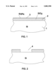
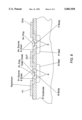
- FIG. 1 is a cross section of a starting wafer coated with oxide and nitride.
- FIG. 2 is a cross section of the first etched opening in the oxide and nitride.
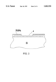
- FIG. 3 shows the regrown oxide in the first opening.
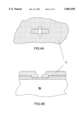
- FIG. 4 shows plane and cross section of the resist pattern defining the second opening.
- FIG. 5 shows plane and cross section of second opening that will be below the MOS channel region.
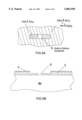
- FIG. 6 shows a cross section after amorphous silicon deposition.
- FIG. 7 shows a cross section after chemical-mechanical polishing.
- FIG. 8 shows, as an application example that uses this invention's starting material, a cross section of a CMOS inverter, after poly gate and junction definition.
- FIG. 1 shows, at the start of the process, a silicon wafer 1 that has grown or deposited onto it silicon dioxide layer 2 with a thickness of 2000 ⁇ , and a very thin layer of silicon nitride 3 deposited on the oxide of 100 ⁇ .
- the wafer is coated with resist which is exposed, developed and baked into a pattern that will define the location of the SOI transistors.
- FIG. 2 shows a cross section view after these steps of one opening 4 of many openings in a typical circuit.
- Oxide is grown to a thickness of 1000 ⁇ in the openings 4 not protected by nitride.
- FIG. 3 shows this result for one opening.
- FIGS. 4A and 4B show the plane view and the cross section view of this patterned resist 5.
- FIGS. 5A and 5B show the results of this etch after resist removal.
- the wafer is next thoroughly cleaned, placed in a reactor, and a thin layer of approximately 1000 ⁇ of amorphous silicon 7 is deposited.
- hydrogen gas should be flowed into the reactor to thoroughly remove any residual oxide on the silicon at the bottom of the openings 6, thereby allowing intimate contact of the amorphous silicon to the single crystal silicon in these regions.
- FIG. 6 shows the results of this operation.
- the wafer is then chemical-mechanically polished to remove the amorphous silicon, with an etch stop provided by the silicon nitride. This leaves only openings 4 with amorphous silicon, which is approximately level with the top surface of the nitride.
- FIG. 7 shows the results of this operation.
- the wafer is annealed at a temperature and for a time sufficient for the amorphous silicon in openings 6 to convert to single crystal silicon, being seeded by the underlying single crystal silicon substrate.
- FIG. 8 shows the cross section of the first steps in forming a CMOS inverter pair.
- the P an N Wells can be implanted before the SOI transistors are formed or after. If formed before, there should be a high temperature step to outdiffuse N dopant from the N Well into the N Body and P dopant from the P Well into the P Body.
- the openings 6 in FIG. 8 are somewhat wider than the transistor source-drain spacings. This is to insure, that even with some small misalignment, the transistor regions directly under the Poly gates will be directly over the silicon substrate, thereby insuring these regions will be converted to single crystal silicon during the high temperature amorphous silicon anneal.
- FIG. 8 is not quite drawn to scale laterally; openings 6 to the silicon substrate, will typically be less than 1/6 of the transistor areas defined by openings 4, resulting in most of the transistor area positioned over oxide rather than over silicon. This will reduce the capacitance of the source and drain junctions, and will allow source and drain contact openings to aluminum to be made with zero misalignment tolerance. Also, adjacent drains or sources can be spaced very closely without worrying about punchthrough. Even adjacent channel regions can be closely spaced if they are both NMOS or both PMOS.
Abstract
The present invention is a technique for producing silicon-on-insulator MOS transistors by damascene patterning of source-drain regions in a thin film of amorphous silicon deposited on a layer of oxide grown on a silicon wafer, where the oxide has previously been etched with a pattern of trenches. In addition, the technique provides for the amorphous layer to contact the underlying silicon substrate through multiple small oxide openings, where subsequent transistor channel regions will align to these openings. After patterning, the wafer is annealed in a high temperature cycle, where the regions of amorphous silicon in contact with the silicon substrate will grow into single crystal silicon suitable for transistor channel regions.
Description
This application is a continuation-in-part of Ser. No. 08/922,864, filed Sep. 3, 1997, which is now abandoned.
1. Field of the Present Invention
The present invention relates to a technique for producing silicon-on-insulator MOS transistors by damascene patterning of a thin film of amorphous silicon deposited on a layer of oxide grown on a silicon wafer, followed by high temperature annealing to form single crystal MOS channel regions.
2. Description of the Prior Art
The primary advantage of using silicon-on-insulator (SOI) substrates, rather than using bulk silicon, for forming MOS transistors has long been recognized as being that of reduced stray capacitance. This allows, of course, higher operating frequencies to be obtained. SOI has other advantages such as better packing density, borderless contacts, latch-up freedom, and radiation hardness.
A thin film of crystalline silicon epitaxially deposited on a polished single crystal aluminum oxide substrate (SOS) was the first composite material to be used for SOI. However, since the crystal properties of aluminum oxide do not perfectly match those of silicon there has always been the problem of reduced yield due to defects in the silicon film.
In recent years SOI circuits have been made by forming a thin film of crystalline silicon on silicon dioxide, where the oxide has been grown on a silicon support wafer. This has enabled the production of silicon films with much lower defect density because the support wafer physical properties, such as thermal expansion coefficient, match those of the silicon film. Currently SOI refers to silicon-on-oxide, which will be our convention.
There are a few different methods for producing SOI substrates; all of which are rather difficult because the silicon film has to be single crystal, and for best performance of the finished circuit, the film should be very thin (less than approximately 1000 Angstroms).
Another difficulty with current SOI is that the MOS transistor body connections are typically left floating for efficiency of chip layout. This can sometimes cause problems. For example, excess charge can remain in a transistor floating body region when attempting to turn a transistor off, which can slow down circuit operation. This problem can be solved by implanting just the right amount of recombination centers in the film; this is difficult to control, because too many centers will degrade the mobility of the film.
It is therefore the object of the present invention to provide a simplified method for producing SOI substrates; and to provide a technique for electrically connecting MOS body regions to well defined voltages without incurring any layout area penalty; and to maintain the high density layout capability of current SOI.
The present invention is a technique for producing silicon-on-insulator MOS transistors by damascene patterning of source-drain regions in a thin film of amorphous silicon deposited on a layer of oxide grown on a silicon wafer, where the oxide has previously been etched with a pattern of trenches. In addition, the invention provides for the amorphous layer to contact the underlying silicon substrate through multiple small oxide openings, where subsequent transistor channel regions will align to these openings. After patterning, the wafer is annealed in a high temperature cycle, where the regions of amorphous silicon in contact with the silicon substrate will grow into single crystal silicon suitable for transistor channel regions.
FIG. 1 is a cross section of a starting wafer coated with oxide and nitride.
FIG. 2 is a cross section of the first etched opening in the oxide and nitride.
FIG. 3 shows the regrown oxide in the first opening.
FIG. 4 shows plane and cross section of the resist pattern defining the second opening.
FIG. 5 shows plane and cross section of second opening that will be below the MOS channel region.
FIG. 6 shows a cross section after amorphous silicon deposition.
FIG. 7 shows a cross section after chemical-mechanical polishing.
FIG. 8 shows, as an application example that uses this invention's starting material, a cross section of a CMOS inverter, after poly gate and junction definition.
The following is a description of a preferred process flow for making the SOI substrates of this invention, where the thicknesses and dimensions given are representative of modern high resolution masking capabilities, and representative of the requirements of a low voltage logic circuit. Other thicknesses and dimensions can used for different situations.
1. FIG. 1 shows, at the start of the process, a silicon wafer 1 that has grown or deposited onto it silicon dioxide layer 2 with a thickness of 2000 Å, and a very thin layer of silicon nitride 3 deposited on the oxide of 100 Å.
2. The wafer is coated with resist which is exposed, developed and baked into a pattern that will define the location of the SOI transistors.
3. Using well known techniques, the nitride is etched followed by an oxide etch to the silicon substrate, followed by resist removal. FIG. 2 shows a cross section view after these steps of one opening 4 of many openings in a typical circuit.
4. Oxide is grown to a thickness of 1000 Å in the openings 4 not protected by nitride. FIG. 3 shows this result for one opening.
5. The wafer is again coated with resist which is exposed, developed and baked into a pattern that will define openings through the oxide that will later align with transistor channel locations. FIGS. 4A and 4B show the plane view and the cross section view of this patterned resist 5.
6. The 1000 Å of oxide in the resist opening that is not over nitride is etched, resulting in openings 6 to the silicon of the substrate; this should preferably be an anisotropic plasma etch that etches oxide much faster than silicon or nitride. FIGS. 5A and 5B show the results of this etch after resist removal.
7. The wafer is next thoroughly cleaned, placed in a reactor, and a thin layer of approximately 1000 Å of amorphous silicon 7 is deposited. Before depositing silicon, hydrogen gas should be flowed into the reactor to thoroughly remove any residual oxide on the silicon at the bottom of the openings 6, thereby allowing intimate contact of the amorphous silicon to the single crystal silicon in these regions. FIG. 6 shows the results of this operation.
8. The wafer is then chemical-mechanically polished to remove the amorphous silicon, with an etch stop provided by the silicon nitride. This leaves only openings 4 with amorphous silicon, which is approximately level with the top surface of the nitride. FIG. 7 shows the results of this operation.
9. After a thorough cleaning, the wafer is annealed at a temperature and for a time sufficient for the amorphous silicon in openings 6 to convert to single crystal silicon, being seeded by the underlying single crystal silicon substrate.
Subsequent processing can proceed using well known procedures. FIG. 8 shows the cross section of the first steps in forming a CMOS inverter pair. The P an N Wells can be implanted before the SOI transistors are formed or after. If formed before, there should be a high temperature step to outdiffuse N dopant from the N Well into the N Body and P dopant from the P Well into the P Body.
The openings 6 in FIG. 8 are somewhat wider than the transistor source-drain spacings. This is to insure, that even with some small misalignment, the transistor regions directly under the Poly gates will be directly over the silicon substrate, thereby insuring these regions will be converted to single crystal silicon during the high temperature amorphous silicon anneal.
The process flow as described results in field regions between transistors having a thickness of 2000 Å. For a modern submicron logic circuit process, with a supply voltage of about 3 volts, and well surface dopings of about 1017 ions/cm3, this should result in high enough field inversion voltages. Other applications might require a thicker field oxide or need field doping.
FIG. 8 is not quite drawn to scale laterally; openings 6 to the silicon substrate, will typically be less than 1/6 of the transistor areas defined by openings 4, resulting in most of the transistor area positioned over oxide rather than over silicon. This will reduce the capacitance of the source and drain junctions, and will allow source and drain contact openings to aluminum to be made with zero misalignment tolerance. Also, adjacent drains or sources can be spaced very closely without worrying about punchthrough. Even adjacent channel regions can be closely spaced if they are both NMOS or both PMOS.
Claims (1)
1. A processing method for forming a silicon-on-insulator (SOI) substrate comprised of the following steps:
a) coating a single crystal silicon wafer with a layer of silicon dioxide (SiO2);
b) partially etching large openings in the SiO2 to a depth less than the SiO2 thickness, where each large opening defines the area of an MOS transistor, including source, drain and channel regions;
c) etching a small opening within each large opening, where the small opening is etched completely through to the underlying silicon substrate, and where the small opening is positioned beneath the channel region of the MOS transistor defined by the large opening;
d) depositing amorphous silicon over the SiO2 to a thickness greater than the SiO2 thickness;
e) chemical-mechanical polishing the wafer to remove the amorphous silicon from the surface of the SiO2 except within the large and small openings;
f) heating the silicon wafer to a temperature sufficient to cause crystallization of the amorphous silicon within the small openings.
Priority Applications (1)
| Application Number | Priority Date | Filing Date | Title |
|---|---|---|---|
| US08/948,211 US5882958A (en) | 1997-09-03 | 1997-10-09 | Damascene method for source drain definition of silicon on insulator MOS transistors |
Applications Claiming Priority (2)
| Application Number | Priority Date | Filing Date | Title |
|---|---|---|---|
| US92286497A | 1997-09-03 | 1997-09-03 | |
| US08/948,211 US5882958A (en) | 1997-09-03 | 1997-10-09 | Damascene method for source drain definition of silicon on insulator MOS transistors |
Related Parent Applications (1)
| Application Number | Title | Priority Date | Filing Date |
|---|---|---|---|
| US92286497A Continuation-In-Part | 1997-09-03 | 1997-09-03 |
Publications (1)
| Publication Number | Publication Date |
|---|---|
| US5882958A true US5882958A (en) | 1999-03-16 |
Family
ID=25447673
Family Applications (1)
| Application Number | Title | Priority Date | Filing Date |
|---|---|---|---|
| US08/948,211 Expired - Fee Related US5882958A (en) | 1997-09-03 | 1997-10-09 | Damascene method for source drain definition of silicon on insulator MOS transistors |
Country Status (1)
| Country | Link |
|---|---|
| US (1) | US5882958A (en) |
Cited By (8)
| Publication number | Priority date | Publication date | Assignee | Title |
|---|---|---|---|---|
| US5939788A (en) * | 1998-03-11 | 1999-08-17 | Micron Technology, Inc. | Copper diffusion barrier, aluminum wetting layer and improved methods for filling openings in silicon substrates with cooper |
| US5970367A (en) * | 1997-10-01 | 1999-10-19 | Wanlass; Frank M. | Double damascene pattering of silcon-on-insulator transistors |
| US6174754B1 (en) | 2000-03-17 | 2001-01-16 | Taiwan Semiconductor Manufacturing Company | Methods for formation of silicon-on-insulator (SOI) and source/drain-on-insulator(SDOI) transistors |
| US6350659B1 (en) | 1999-09-01 | 2002-02-26 | Agere Systems Guardian Corp. | Process of making semiconductor device having regions of insulating material formed in a semiconductor substrate |
| US20060005902A1 (en) * | 2002-04-22 | 2006-01-12 | Hans-Joachim Barth | Method for production of thin metal-containing layers having low electrical resistance |
| US20070020828A1 (en) * | 2005-07-13 | 2007-01-25 | Seiko Epson Corporation | Method for manufacturing semiconductor apparatus and the semiconductor apparatus |
| US20080070372A1 (en) * | 2006-09-19 | 2008-03-20 | Samsung Electronics Co., Ltd. | Method of manufacturing a semiconductor device |
| US9324873B2 (en) * | 2013-12-30 | 2016-04-26 | Boe Technology Group Co., Ltd. | Fabricating method of thin film transistor, thin film transistor and display panel |
Citations (6)
| Publication number | Priority date | Publication date | Assignee | Title |
|---|---|---|---|---|
| US3528168A (en) * | 1967-09-26 | 1970-09-15 | Texas Instruments Inc | Method of making a semiconductor device |
| US5116771A (en) * | 1989-03-20 | 1992-05-26 | Massachusetts Institute Of Technology | Thick contacts for ultra-thin silicon on insulator films |
| US5213991A (en) * | 1986-02-07 | 1993-05-25 | Nippon Telegraph And Telephone Corporation | Method of manufacturing semiconductor device |
| US5338697A (en) * | 1989-12-01 | 1994-08-16 | Seiko Instruments Inc. | Doping method of barrier region in semiconductor device |
| US5618741A (en) * | 1994-04-07 | 1997-04-08 | U.S. Philips Corporation | Manufacture of electronic devices having thin-film transistors |
| US5670398A (en) * | 1994-12-26 | 1997-09-23 | Hyundai Electronics Industries Co., Ltd. | Method of manufacturing thin film transistor having a double channel |
-
1997
- 1997-10-09 US US08/948,211 patent/US5882958A/en not_active Expired - Fee Related
Patent Citations (6)
| Publication number | Priority date | Publication date | Assignee | Title |
|---|---|---|---|---|
| US3528168A (en) * | 1967-09-26 | 1970-09-15 | Texas Instruments Inc | Method of making a semiconductor device |
| US5213991A (en) * | 1986-02-07 | 1993-05-25 | Nippon Telegraph And Telephone Corporation | Method of manufacturing semiconductor device |
| US5116771A (en) * | 1989-03-20 | 1992-05-26 | Massachusetts Institute Of Technology | Thick contacts for ultra-thin silicon on insulator films |
| US5338697A (en) * | 1989-12-01 | 1994-08-16 | Seiko Instruments Inc. | Doping method of barrier region in semiconductor device |
| US5618741A (en) * | 1994-04-07 | 1997-04-08 | U.S. Philips Corporation | Manufacture of electronic devices having thin-film transistors |
| US5670398A (en) * | 1994-12-26 | 1997-09-23 | Hyundai Electronics Industries Co., Ltd. | Method of manufacturing thin film transistor having a double channel |
Cited By (10)
| Publication number | Priority date | Publication date | Assignee | Title |
|---|---|---|---|---|
| US5970367A (en) * | 1997-10-01 | 1999-10-19 | Wanlass; Frank M. | Double damascene pattering of silcon-on-insulator transistors |
| US5939788A (en) * | 1998-03-11 | 1999-08-17 | Micron Technology, Inc. | Copper diffusion barrier, aluminum wetting layer and improved methods for filling openings in silicon substrates with cooper |
| US6204179B1 (en) | 1998-03-11 | 2001-03-20 | Micron Technology, Inc. | Copper diffusion barrier, aluminum wetting layer and improved methods for filling openings in silicon substrates with copper |
| US6350659B1 (en) | 1999-09-01 | 2002-02-26 | Agere Systems Guardian Corp. | Process of making semiconductor device having regions of insulating material formed in a semiconductor substrate |
| US6174754B1 (en) | 2000-03-17 | 2001-01-16 | Taiwan Semiconductor Manufacturing Company | Methods for formation of silicon-on-insulator (SOI) and source/drain-on-insulator(SDOI) transistors |
| US20060005902A1 (en) * | 2002-04-22 | 2006-01-12 | Hans-Joachim Barth | Method for production of thin metal-containing layers having low electrical resistance |
| US20070020828A1 (en) * | 2005-07-13 | 2007-01-25 | Seiko Epson Corporation | Method for manufacturing semiconductor apparatus and the semiconductor apparatus |
| US7316943B2 (en) * | 2005-07-13 | 2008-01-08 | Seiko Epson Corporation | Method for manufacturing semiconductor apparatus having drain/source on insulator |
| US20080070372A1 (en) * | 2006-09-19 | 2008-03-20 | Samsung Electronics Co., Ltd. | Method of manufacturing a semiconductor device |
| US9324873B2 (en) * | 2013-12-30 | 2016-04-26 | Boe Technology Group Co., Ltd. | Fabricating method of thin film transistor, thin film transistor and display panel |
Similar Documents
| Publication | Publication Date | Title |
|---|---|---|
| EP0166218B1 (en) | Silicon-on-insulator transistors | |
| US6900094B2 (en) | Method of selective removal of SiGe alloys | |
| US5891763A (en) | Damascene pattering of SOI MOS transistors | |
| CN100411180C (en) | Semiconductor structure and method for manufacturing semiconductor structure | |
| US4686758A (en) | Three-dimensional CMOS using selective epitaxial growth | |
| US4110899A (en) | Method for manufacturing complementary insulated gate field effect transistors | |
| US4755481A (en) | Method of making a silicon-on-insulator transistor | |
| US4704302A (en) | Process for producing an insulating layer buried in a semiconductor substrate by ion implantation | |
| US4654958A (en) | Process for forming isolated silicon regions and field-effect devices on a silicon substrate | |
| JPH05160396A (en) | Mos field effect transistor | |
| KR19980033016A (en) | Semiconductor Integrated Circuit Manufacturing Method | |
| US4923826A (en) | Method for forming dielectrically isolated transistor | |
| US6617202B2 (en) | Method for fabricating a full depletion type SOI device | |
| US5185286A (en) | Process for producing laminated semiconductor substrate | |
| US5445107A (en) | Semiconductor device and method of formation | |
| US5927992A (en) | Method of forming a dielectric in an integrated circuit | |
| US5882958A (en) | Damascene method for source drain definition of silicon on insulator MOS transistors | |
| Neudeck et al. | Multiple layers of silicon-on-insulator for nanostructure devices | |
| US6074904A (en) | Method and structure for isolating semiconductor devices after transistor formation | |
| US5970367A (en) | Double damascene pattering of silcon-on-insulator transistors | |
| US6933590B2 (en) | Semiconductor device comprising plurality of semiconductor areas having the same top surface and different film thicknesses and manufacturing method for the same | |
| US5053345A (en) | Method of edge doping SOI islands | |
| US6323073B1 (en) | Method for forming doped regions on an SOI device | |
| US6445043B1 (en) | Isolated regions in an integrated circuit | |
| US4722912A (en) | Method of forming a semiconductor structure |
Legal Events
| Date | Code | Title | Description |
|---|---|---|---|
| REMI | Maintenance fee reminder mailed | ||
| LAPS | Lapse for failure to pay maintenance fees | ||
| STCH | Information on status: patent discontinuation |
Free format text: PATENT EXPIRED DUE TO NONPAYMENT OF MAINTENANCE FEES UNDER 37 CFR 1.362 |
|
| FP | Lapsed due to failure to pay maintenance fee |
Effective date: 20030316 |