US5869214A - Color image forming apparatus and color image forming method thereof - Google Patents
Color image forming apparatus and color image forming method thereof Download PDFInfo
- Publication number
- US5869214A US5869214A US08/895,991 US89599197A US5869214A US 5869214 A US5869214 A US 5869214A US 89599197 A US89599197 A US 89599197A US 5869214 A US5869214 A US 5869214A
- Authority
- US
- United States
- Prior art keywords
- toner
- image
- latent image
- color
- electric potential
- Prior art date
- Legal status (The legal status is an assumption and is not a legal conclusion. Google has not performed a legal analysis and makes no representation as to the accuracy of the status listed.)
- Expired - Lifetime
Links
Images


Classifications
-
- G—PHYSICS
- G03—PHOTOGRAPHY; CINEMATOGRAPHY; ANALOGOUS TECHNIQUES USING WAVES OTHER THAN OPTICAL WAVES; ELECTROGRAPHY; HOLOGRAPHY
- G03G—ELECTROGRAPHY; ELECTROPHOTOGRAPHY; MAGNETOGRAPHY
- G03G15/00—Apparatus for electrographic processes using a charge pattern
- G03G15/50—Machine control of apparatus for electrographic processes using a charge pattern, e.g. regulating differents parts of the machine, multimode copiers, microprocessor control
- G03G15/5033—Machine control of apparatus for electrographic processes using a charge pattern, e.g. regulating differents parts of the machine, multimode copiers, microprocessor control by measuring the photoconductor characteristics, e.g. temperature, or the characteristics of an image on the photoconductor
- G03G15/5037—Machine control of apparatus for electrographic processes using a charge pattern, e.g. regulating differents parts of the machine, multimode copiers, microprocessor control by measuring the photoconductor characteristics, e.g. temperature, or the characteristics of an image on the photoconductor the characteristics being an electrical parameter, e.g. voltage
-
- G—PHYSICS
- G03—PHOTOGRAPHY; CINEMATOGRAPHY; ANALOGOUS TECHNIQUES USING WAVES OTHER THAN OPTICAL WAVES; ELECTROGRAPHY; HOLOGRAPHY
- G03G—ELECTROGRAPHY; ELECTROPHOTOGRAPHY; MAGNETOGRAPHY
- G03G15/00—Apparatus for electrographic processes using a charge pattern
- G03G15/01—Apparatus for electrographic processes using a charge pattern for producing multicoloured copies
-
- G—PHYSICS
- G03—PHOTOGRAPHY; CINEMATOGRAPHY; ANALOGOUS TECHNIQUES USING WAVES OTHER THAN OPTICAL WAVES; ELECTROGRAPHY; HOLOGRAPHY
- G03G—ELECTROGRAPHY; ELECTROPHOTOGRAPHY; MAGNETOGRAPHY
- G03G2215/00—Apparatus for electrophotographic processes
- G03G2215/00025—Machine control, e.g. regulating different parts of the machine
- G03G2215/00029—Image density detection
- G03G2215/00033—Image density detection on recording member
- G03G2215/00037—Toner image detection
- G03G2215/00042—Optical detection
-
- G—PHYSICS
- G03—PHOTOGRAPHY; CINEMATOGRAPHY; ANALOGOUS TECHNIQUES USING WAVES OTHER THAN OPTICAL WAVES; ELECTROGRAPHY; HOLOGRAPHY
- G03G—ELECTROGRAPHY; ELECTROPHOTOGRAPHY; MAGNETOGRAPHY
- G03G2215/00—Apparatus for electrophotographic processes
- G03G2215/00025—Machine control, e.g. regulating different parts of the machine
- G03G2215/00029—Image density detection
- G03G2215/00033—Image density detection on recording member
- G03G2215/00054—Electrostatic image detection
Definitions
- the present invention relates to a color image forming apparatus and a color image forming method thereof to form a color toner image on a recording medium such as a sheet of paper by an electrophotographic method or an electrostatic recording method.
- an electrophotographic method or an electrostatic recording method by which a two-color or a multi-color image can be printed when an electric charge latent image of multi-value is formed on a photoconductive photoreceptor or a dielectric body and the thus formed latent image is printed on a sheet of paper using a plurality of toners of different colors.
- the present invention has been accomplished to solve the conventional problems. It is an object of the present invention to provide a color image forming apparatus and a color image forming method thereof characterized in that: it is diagnosed that the image forming apparatus is in a state in which only the information to be recorded can be printed by the image forming apparatus, so that recording paper and toner can not be wasted, and confirmation work of printing can be reduced or completely avoided.
- the first embodiment of invention is to provide a color image forming apparatus comprising:
- a latent image forming means for forming an electrostatic latent image having at least three electric potential levels, on a first recording body
- a developing means for developing the latent image with toner, the polarity of which is different from that of the latent image, so as to form at least a two-color toner image
- a transfer means for transferring the toner image on a second recording body
- a cleaning means for removing residual toner and electric charge from the first recording body, wherein a color image is continuously formed by the latent image forming means, developing means, transfer means and cleaning means.
- the color image forming apparatus further comprises:
- a surface electric potential measuring means such as an electric potential sensor for measuring a surface electric potential in a region outside the latent image forming region on the first recording body
- a comparing means such as a portion of a controller for comparing a measured value measured by the surface electric potential measuring means with a predetermined value of the surface electric potential
- control means such as a controller for controlling the start of color image formation on a recording sheet when the measured value is lower than the predetermined value as a result of the comparison.
- the second embodiment of invention is to provide a color image forming apparatus comprising:
- a latent image forming means for forming an electrostatic latent image having at least three electric potential levels, on a first recording body
- a developing means for developing the latent image with toner, the polarity of which is different from that of the latent image, so as to form at least a two-color toner image
- a transfer means for transferring the toner image on a second recording body such as a sheet of paper or dielectric film;
- a cleaning means for removing residual toner and electric charge from the first recording body, wherein a color image is continuously formed by the latent image forming means, developing means, transfer means and cleaning means.
- the color image forming apparatus further comprises:
- a toner adhesion quantity measuring means such as an optical toner sensor and a toner electric charge sensor for measuring a quantity of adhering toner in a region outside the latent image forming region on the first recording body;
- a comparing means such as a portion of the controller for comparing a measured value measured by the toner adhesion quantity measuring means with a predetermined value of a quantity of adhering toner
- control means such as a controller for controlling the start of color image formation on a recording sheet when the measured value is lower than the predetermined value as a result of the comparison.
- the third embodiment of invention is to provide a color image forming method comprising:
- a latent image forming process for forming an electrostatic latent image having at least three electric potential levels, on a first recording body
- a transfer process for transferring the toner image on a second recording body such as a sheet of paper and dielectric film
- the color image forming method further comprises:
- a surface electric potential measuring process such as an electric potential sensor for measuring a surface electric potential in a region outside the latent image forming region on the first recording body;
- a comparing process for comparing a measured value measured by the surface electric potential measuring process with a predetermined value of the surface electric potential
- control process for controlling the start of color image formation on a recording sheet when the measured value is lower than the predetermined value as a result of the comparison.
- the fourth embodiment of invention is to provide a color image forming method comprising:
- a latent image forming process for forming an electrostatic latent image having at least three electric potential levels, on a first recording body
- a transfer process for transferring the toner image on a second recording body such as a sheet of paper and dielectric film
- the color image forming method further comprises:
- a toner adhesion quantity measuring process such as an optical toner sensor and a toner electric charge sensor for measuring a quantity of adhering toner in a region outside the latent image forming region on the first recording body;
- a comparing process for comparing a measured value measured by the toner adhesion quantity measuring process with a predetermined value of a quantity of adhering toner
- control process for controlling the start of color image formation on a recording sheet when the measured value is lower than the predetermined value as a result of the comparison.
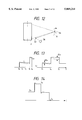
- FIG. 1 is an arrangement view showing an outline of the image forming section of the two-color image forming apparatus of the embodiment of the present invention
- FIGS. 2A to 2C are schematic illustrations to show an electric charge level of the electric charge latent image of multi-value
- FIG. 3 is a characteristic diagram showing a relation between the quantity of laser beams and the surface voltage of a photoreceptor
- FIG. 4 is a characteristic diagram showing a relation between the drive current of a semiconductor laser and the quantity of emitted laser beams
- FIGS. 5A to 5E are views showing a model of the relation among the original image to be recorded, the signal current, the quantity of emitted laser beams, the distribution of latent image electric charges, and the distribution of the latent image electric field, respectively;
- FIGS. 6A to 6C are views to explain the circumstances of a fringe image generated in the process of printing
- FIG. 7 is a view showing another example of the fluctuation of voltage in the background.
- FIG. 8 is a graph showing an example of the charging characteristic of the single layer type positive polarity organic photoconductive photoreceptor
- FIG. 9 is a characteristic diagram showing a relation between the background voltage and the fringe image density in the case where a two-component type magnetic developer is used.
- FIG. 10 is a characteristic diagram showing a relation between the toner electric charge and the fringe image density in the case where a two-component type magnetic developer is used;
- FIG. 11 is a characteristic diagram showing a relation between the dynamic electric resistance of a developer and the fringe image density and also showing a relation between the dynamic electric resistance of the developer and the number of adhering carrier particles in the case where a two-component type magnetic developer is used;
- FIG. 12 is a schematic illustration showing a state in which optical scanning is conducted on the photoreceptor by laser beams
- FIG. 13 is a schematic illustration showing a change in the quantity of light of a recording signal at the time t in the optical scanning process
- FIG. 14 is a schematic illustration showing a deformed waveform of the drive current
- FIG. 15 is a block diagram showing a preferable control circuit to control a quantity of light emitted from the laser
- FIG. 16 is a timing chart of each signal shown in FIG. 15;
- FIGS. 17A to 17D are schematic illustrations showing an initial pattern used in the process of initial operation suitable for executing the present invention, respectively;
- FIG. 18 is a schematic illustration showing an example of the procedure of the initial operation process according to the present invention.
- FIG. 19 is an arrangement view showing an outline of the image forming section of the color image forming apparatus of another embodiment of the present invention in which a two-component developer is used as a developing system to develop three electric latent images;
- FIG. 20 is a circuit diagram to explain a method of measuring a dynamic electric resistance of a two-component magnetic developer and also a method of measuring an electric charge of toner;
- FIG. 21 is an arrangement view showing an outline of the image forming section of the image forming apparatus of still another embodiment of the present invention into which an amorphous silicon photoreceptor drum is incorporated;
- FIG. 22 is an arrangement view showing an outline of the image forming section of the image forming apparatus of still another embodiment of the present invention in which one-component type nonmagnetic developer is used.
- the present invention comprises a means for judging that a fringe image different from the information to be originally recorded is not generated in the recording condition.
- the present invention comprises an initial operation process in which the image forming motion is repeatedly conducted by a prescribed number of times without transferring a toner image onto the second recording body.
- This operation is more specifically described as follows. Before conducting a printing operation, image forming processes except for the transferring process are repeatedly conducted, that is, the processes of latent image formation, development and cleaning are repeatedly conducted. In an image forming apparatus in which a sheet of recording paper, which is the second recording body, is conveyed to a transfer section by a dielectric belt, the dielectric belt is retracted from the photoreceptor, which is the first recording body, at this time.
- the information to be originally recorded is a recording condition in which a different fringe image is not generated. It is judged by measuring the photoreceptor voltage and (or) the quantity of adhering toner.
- measurement of the photoreceptor voltage is conducted in such a manner that fluctuation of the electric potential on the surface of the background of the photoreceptor is directly measured by an electric potential sensor.
- Measurement of the quantity of adhering toner is conducted in such a manner that the quantity of adhering toner in the background of the photoreceptor is measured by an optical toner sensor or a toner electric charge sensor.
- the measurement of the quantity of adhering toner is an indirect measurement of the fluctuation of the surface electric potential in the background of the photoreceptor, that is, the measurement of the quantity of adhering toner is to measure a quantity of toner caused by photographic fog in the fringe portion.
- the present invention relates to an image forming apparatus and image forming method to obtain a color image from an electric charge latent image of multi-value formed on an insulating recording body by the electrostatic recording method or electrophotographic method.
- the electric charge latent image of multi-value is illustrated in FIGS. 2A to 2C.
- FIG. 2A is a schematic illustration showing an example of three electric charge latent images having an electric charge density ⁇ 1 of the positive polarity and an electric charge density ⁇ 2 of the negative polarity, wherein a boundary of the positive and negative polarity is zero (0) that corresponds to the background. That is, FIG. 2A is a schematic illustration showing an example of image formation conducted by toners of the negative and the positive polarity, the colors of which are different from each other, with respect to the electric charge density al and the electric charge density ⁇ 2.
- FIG. 2B is a schematic illustration showing an example of three electric charge latent images having electric charge density ⁇ 3, ⁇ 4 and ⁇ 5 of the positive polarity.
- the electric charge density of the background is ⁇ 4
- image formation is conducted when toner of the negative polarity and toner of the positive polarity, the colors of which are different from each other, are made to adhere onto portions corresponding to the electric charge density of ⁇ 3 and ⁇ 5.
- FIG. 2C is a schematic illustration showing an example of an electric charge latent image of 4 values having electric charge density ⁇ 6, ⁇ 7, ⁇ 8 and ⁇ 9 of the positive polarity.
- the electric charge density of the background is ⁇ 8, and image formation is conducted when the first toner of the negative polarity is made to adhere to a portion corresponding to ⁇ 9, the second toner of the positive polarity and the third toner of the positive polarity, the color of which is different from the colors of the first and the second toner, which are made to adhere to a portion corresponding to ⁇ 6, and the third toner is made to adhere to portion corresponding to ⁇ 7.
- FIG. 1 is an arrangement view showing an outline of the image forming apparatus of the embodiment of the present invention to use an electrophotographic method by which a latent image illustrated in FIG. 2B is formed on a photoconductive photoreceptor that is the first recording body, and a color image of two colors is printed on a sheet of paper that is the second recording body.
- the first recording body is composed of a drum base body 1 and a belt-shaped organic photoconductive photoreceptor 2 which is wound around the drum base body 1.
- the photoreceptor 2 is fed from the drum base body 1. After it has been used, it is accommodated again in the drum base body 1.
- a surface of the photoreceptor 2 provided on the drum base body 1 is subjected to corona charge by a charger (C1) 3, so that the surface of the photoreceptor 2 can be uniformly charged.
- Moving speed of the photoreceptor 2 is determined by a predetermined printing speed. In general, in this type printer, the moving speed of the photoreceptor 2 is 10 to 50 cm/s. However, it should be noted that the moving speed of the photoreceptor 2 is not limited to the specific value.
- the charger (C1) 3 has a grid 4 to control the charging voltage.
- the corona wire of the charger (C1) 3 is connected with a power supply of high voltage (H1) 5, and the grid 4 of the charger (C1) 3 is connected with a grid power supply 6.
- laser beams 8 emitted from a laser beam source 7 are irradiated on the surface of the photoreceptor 2. Due to the foregoing, an electric charge latent image corresponding to information to be recorded is formed on the photoreceptor 2.
- the laser beam source 7 is driven by a signal sent from a recording signal source 9.
- the electric latent image illustrated in FIG. 2B is formed so as to form a toner image of two types (for example, two colors).
- a charging voltage of the charger (C1) 3 and a quantity of light of laser beams 8 are controlled so that the electric charge latent image can be properly formed in a predetermined range.
- a surface voltage of the photoreceptor 2 is measured with an electric potential sensor 10 in such a manner that a surface voltage corresponding to at least ⁇ 4 (corresponding to the background) in FIG. 2B is measured.
- the grid power supply 6 and the laser beam source 7 are controlled with a controller 11 so that the voltage in the background can be maintained in a predetermined range.
- the thus obtained electric charge latent image is developed with two types of color toners, for example, black toner and chromatic color toner.
- color toners for example, black toner and chromatic color toner.
- the first development is conducted by means of a normal development with color toner and the second development is conducted by means of a reversal development with black toner.
- a color developing roller 12 to which color toner (for example, red toner) is attracted by a magnetic force, is arranged close to the photoreceptor 2 so that the color toner can be contacted with the photoreceptor 2 or alternatively the color toner can be located close to the photoreceptor 2.
- This color developing roller 12 is connected to a bias power supply 13, so that bias voltage V b1 can be impressed upon the color developing roller 12.
- a black developing roller 14, to which black toner is attracted by a magnetic force, is arranged close to the photoreceptor 2 so that the black toner can be contacted with the photoreceptor 2 or alternatively the black toner can be located close to the photoreceptor 2.
- the black developing roller 14 is connected to a bias voltage 15, so that bias voltage V b2 can be impressed upon the black developing roller 14.
- the bias power supplies 13, 15 are respectively connected to AC power supply (AC1) 16, and AC bias voltage is superimposed on the bias power supplies 13, 15.
- the frequency of AC power supply 16 is 200 to 5000 Hz
- the effective voltage of AC power supply 16 is 100 to 1000 V.
- the reason why AC bias voltage is superimposed on the bias power supplies 13, 15 is to facilitate the development, suppress the occurrence of fog, and prevent the adhesion of different toner to the roller. Therefore, the superimposition of AC bias voltage is not necessarily needed.
- the superimposition of AC bias voltage is effective.
- AC voltage may be impressed only upon the black developing roller 14.
- color toner the polarity of which is negative, normal development is conducted by the color developing roller 12, so that a color toner image can be formed.
- black toner the polarity of which positive, a black toner image is formed by the black developing roller 14.
- the intensity of bias voltage V b1 and the intensity of bias voltage V b2 will be described later.
- the charging polarity may be either positive or negative.
- a positive power supply of high voltage (H2) 18 and an AC power supply (AC2) 19 AC voltage, the frequency of which is 200 to 5000 Hz and the effective voltage of which is 0.5 to 3 kV, is superimposed on DC voltage, the voltage of which is 4 to 7 kV. The thus obtained voltage is impressed so as to generate a corona discharge.
- Superimposition of AC voltage on DC voltage is conducted for facilitating the uniformity of electric charging. Therefore, it is possible to omit superimposition of AC voltage on DC voltage.
- a sheet of recording paper 22 is conveyed by a sheet feed roller 23 and moved in conjunction with a dielectric belt 24. While the sheet of recording paper 22 is coming into contact with the photoreceptor 2, toner images of two colors are simultaneously transferred onto the sheet of recording paper 22 by a transfer unit 25. At this time, the transfer unit 25 is connected with a power supply (H3) 26 of high voltage. Therefore, a negative corona electric charge is given to the dielectric belt 24, so that a transfer electric field is formed. After transfer has been completed, the sheet of recording paper 32 is moved in conjunction with the dielectric belt 24. After that, the sheet of recording paper 32 is separated from the dielectric belt 24.
- H3 power supply
- the charger (C3) 27 is connected to a power supply (H4) 28 of high voltage and an AC power supply (AC3) 29.
- AC voltage the frequency of which is 200 to 5000 Hz and the effective voltage of which is 0.5 to 3 kV, and DC voltage of 4 to 7 kV are superimposed on each other, and the thus superimposed voltage is impressed upon the charger (C3) 27 so as to generate corona.
- AC voltage is superimposed is to facilitate the uniformity of electric charging and extend an allowable range with respect to the fluctuating factors such as a type of sheet, a state of separation, and an environmental temperature and humidity. Depending upon the operating conditions, it is possible to omit the superimposition of AC voltage on DC voltage.
- toner adheres to a portion on the dielectric belt 24 between sheets of recording paper to be conveyed. Polarity of the adhering toner on the dielectric belt 24 becomes negative when an electric charge is given by the charger (C3) 27.
- This toner is electrically and mechanically removed by a cleaner (CL1) 30.
- This cleaner (CL1) 30 is connected to a cleaner power supply (C b1 ) 31 and a voltage of 200 to 1000 V is impressed upon it.
- the toner image on the sheet of recording paper 32 is heated and pressured by a fixing unit composed of a heater 33, heat roller 34 and backup roller 35.
- Residual toner on the photoreceptor 2 is electrically charged again by a charger (C4) 38.
- the charging polarity of residual toner is determined to be a polarity sensitive to the photoreceptor 2.
- the charging polarity of residual toner is the same as that given by the charger (C1) 3.
- the charging polarity of residual toner is positive.
- the charger (C4) 38 is connected to a power supply (H5) 39 of high voltage and an AC power supply (AC4) 40.
- AC voltage the frequency of which is 200 to 5000 Hz and the effective voltage of which is 0.5 to 3 kV, and DC voltage of 4 to 7 kV are superimposed on each other, and the thus superimposed voltage is impressed upon the charger (C4) 38 so as to generate corona.
- the reason why AC voltage is superimposed is to facilitate the uniformity of electric charging and extend an allowable range with respect to the fluctuating factors such as an environmental temperature and humidity. Depending upon the operating conditions, it is possible to omit the superimposition of AC voltage on DC voltage.
- the residual toner on the photoreceptor 2 After the residual electric charge on the photoreceptor 2 has been erased by the action of a discharge lamp 412, the residual toner is electrically and mechanically removed by a cleaner (CL2) 42.
- the cleaner (CL2) 42 is connected to a cleaner power supply (C b2 ) 43, and a voltage of 200 to 1000 V, the polarity of which is reverse to the polarity of the electric charge of toner, is impressed upon the cleaner (CL2) 42.
- This voltage to be impressed upon the cleaner (CL2) 42 is adjusted in such a manner that the voltage is low when a quantity of toner is small in a normal printing operation and that the voltage is high when a quantity of toner is large in the case of solving a problem or in the process of initial setting. In this way, the photoreceptor 2 is prepared for the successive printing operation, and it becomes possible to conduct printing operation continuously.
- An electric potential sensor 10 is used for controlling the surface voltage of the photoreceptor 2. In order to prevent the sensitivity of the electric potential sensor 10 from being affected by a change with time, it is preferable to compare an output voltage of the sensor with a reference voltage at all times.
- a drum cap to close up a cutout portion of the photoreceptor 2 is made of conductive or semiconductive material, and when this drum cap is maintained at a predetermined voltage, the above object can be accomplished. Specifically, this voltage is detected by the electric potential sensor 10 and compared with the reference voltage.
- the drum cap is connected with a constant voltage element 46, condenser 45 and resistor 44, so that it is possible to obtain a constant voltage.
- the resistor 44 is a safety resistor to leak an electric charge accumulated in the condenser when maintenance is conducted on the drum after the printing operation has been completed. It is preferable that a switch is added to the circuit and the resistor is activated by turning on the switch only when necessary.
- the present invention has been achieved to accomplish the following objects. Before a normal printing operation, it is diagnosed whether or not the image forming apparatus is in a state in which only information to be recorded can be printed; printing operation is stopped when the printing condition is out of a normal operating range in the process of printing; and the life of a photoreceptor and developer is judged.
- an electric potential sensor 10 toner sensor 37 or toner electric charge sensor 36, and counter 47.
- the dielectric belt 24 is retracted so that it can not be contacted with the photoreceptor 2, or alternatively the transfer unit 25 is put into a condition in which the transfer unit 25 can not be operated, and the latent image forming process, developing process and cleaning process are repeated by a predetermined number of times under the condition that no sheets of recording paper 22 are conveyed.
- the transfer unit 25 may be operated and no sheets of recording paper 22 are conveyed.
- the charging voltage given by the charger (C1) 3 and the background voltage of which are changed by the operation of transfer corona the aforementioned operation is preferably adopted.
- the electric potential of the photoreceptor is measured by the electric potential sensor 10, and also the electric charge of the toner and the resistance of the developer are measured, and adjustment is conducted so that the operation can be normally carried out.
- the printing operation is stopped.
- a sheet of recording paper 22 may be fed in the middle or at the last of the above initial operating process, and printing may be actually conducted on the sheet of recording paper 22.
- the charger (C2) 17 is not operated and the discharging lamp 411 is operated, and the quantity of toner is calculated by measuring a difference between the electric potential of the toner portion and the electric potential of the peripheral portion.
- the above initial operation may be omitted or the time of the above initial operation may be changed. Due to the foregoing, it is possible to enhance the printing efficiency.
- a counter 47 is used for calculating a quantity of toner used in the initial operation, a number of sheets of recording paper, a period of time in which the developer and the photoreceptor 2 are used, and a number of printed sheets.
- the result of calculation is used as data of the toner consumption, the rebate of the charge of recording sheets, the judgment of life of the developer and photoreceptor, and the corrected program of the normal operating condition in accordance with the history of printing.
- the toner sensor 371 can control the image forming apparatus as follows.
- the toner sensor 371 forms a measuring pattern between sheets of recording paper provided on the dielectric belt 24.
- the toner sensor 371 continuously or intermittently measures whether or not it is possible to record an image in a normal condition. As a result of the measurement, it controls the image forming apparatus.
- printing can be accomplished without fail, and further it is possible to suppress a waste of toner or reduce the consumption of sheets of recording paper 22, and furthermore it is possible to the enhance efficiency by reducing the printing time.
- FIG. 3 is a graph showing a relation between a quantity of the laser beams 8 and a surface voltage of the photoreceptor 2.
- the charger (C1) 3 electrically charges a surface of the photoreceptor 2, so that the surface voltage can be raised to V 0 .
- V 0 600 to 1200 V.
- L c usually, zero
- L h and L k the surface voltage becomes V 0 , V h and V k in accordance with the optical attenuating characteristic of the photoreceptor 2.
- V k is a factor substantially determined by the residual voltage characteristic of the photoreceptor 2.
- V k is 50 to 150 V.
- a semiconductor laser is used for the laser beam source 7, it is possible to reduce the dimensions of the apparatus and it is also possible to reduce the manufacturing cost.
- FIG. 4 is a graph showing a relation between a drive current (signal current) of the semiconductor laser and a quantity of light emitted by the laser.
- S c , S h and S k shown on the graph respectively represent the signal currents of the color portion, the background portion and the black portion.
- L 0i , L hi and L ki represent quantities of emitted light corresponding to them.
- FIGS. 5A to 5E are views showing a model of the relation among the original image to be recorded (FIG. 5A), the signal current (FIG. 5B), the quantity of emitted laser beams (FIG. 5C), the distribution of latent image electric charges (FIG. 5D) and the distribution of the latent image electric field (FIG. 5E).
- FIG. 5B When a scanning line is resolved along a one-dotted chain line in the case of recording a red portion 48 and black portion 49, a relation between the signal current and the time t is expressed in FIG. 5B.
- FIG. 5C When the photoreceptor is scanned by laser beams, a quantity of irradiating light is expressed in FIG. 5C.
- L c , L h and L k in the view respectively represent quantities of irradiating light in the red portion, the background and the black portion.
- FIG. 5D Reference characters in the view respectively express surface voltages when the electric charge density at each level is uniformly distributed in a portion of a large area.
- reference characters V 01 , V h1 and V k1 are respectively voltages of the red portion, the background and the black portion.
- V hn is a reference voltage of the background portion.
- V b1 and V b2 are bias voltage levels to be impressed upon the color developing roller 12 and the black developing roller 14.
- FIG. 5E shows a latent image electric field distribution in the developing section.
- E 01 , E h1 , E k1 , E b1 , E b2 and E hn respectively correspond to V 01 , V h1 , V k1 , V b1 , V b2 and V hn .
- the latent image electric field generates an edge effect at the end portion.
- V b1 and V b2 are determined so that redundant toner images except for information to be recorded, such as fog of an image in the background, ghost and fringe are not generated.
- an intensity of the electric field is close to or higher than E b1 and E b2 by the edge effect in the background, the toner adheres to this portion, and a fringe image is formed, which causes a problem in the image formation.
- FIGS. 6A to 6C are views to explain the circumstances of a fringe image generated in the process of printing.
- V 0 is raised to V 02 and the background voltage V h1 is changed to V h2 being shifted from the predetermined value V hn by ⁇ V hm . Therefore, the end portion electric fields 50, 51 of the background electric field E h2 become close to or higher than E b1 .
- E b1 -E hn , and E hn -E b2 may be increased.
- E 02 -E b1 , and E b2 -E k2 so as to obtain an image of high density. Therefore, the increase in E b1 -E hn and E hn -E b2 is limited.
- V 0 1000 V
- V k 100 V
- V b2 350 to 400 V
- a voltage equivalent value of a quantity of change in the end portion in the background electric field is 50 to 100 V when it is found by changing V b1 or V b2 so as to check the appearance of a fringe image.
- the value of ⁇ V hm is maintained to be 50 to 150 V, that is, the value of ⁇ V hm is approximately 100 V.
- the allowable range of fluctuation is approximately ⁇ 10%.
- FIG. 7 is a view showing another example of the fluctuation of voltage in the background.
- a period of the fluctuation of ⁇ V h is short. This fluctuation is caused by the partial fluctuation of the characteristic of the photoreceptor, the characteristic of the laser drive circuit, and the influence of noise. Due to the fluctuation, the generation of a fringe image and the occurrence of fog in the background are facilitated, and further image unevenness is caused by the fluctuation.
- ⁇ V h is suppressed in a range of about ⁇ 10%.
- Examples of usable photoreceptors of the present invention are: selenium photoconductor, amolphous silicon photoconductor, zinc oxide photoconductor, and organic photoconductor. It is preferable to use a single layer type positive polarity organic photoconductor, which is made as follows.
- phthalocyanine pigment is used as an electric charge generating agent
- perylene pigment is preferably used as an electric charge generating agent. It is dispersed in resin such as polycarbonate together with an electric charge carrying material such as polyvinylcarbazole and hydrazone, and an additive such as sensitizer and deactivation agent. Then, it is coated by the thickness of 20 to 60 ⁇ m.
- the photoreceptor is characterized in that: charging can be uniformly conducted by means of corona charging; a quantity of generated ozone is small; resolution is high; and the manufacturing cost is low.
- this organic photoconductive photoreceptor When this organic photoconductive photoreceptor is subjected to humidity saturation treatment after it has been heated and dried in the manufacturing process, it is possible to reduce a change in the characteristic caused by an environmental change when it is put into practical use.
- the charging characteristic, sensitivity and residual voltage of the photoconductive photoreceptor are changed according to the frequency of use and the history of use.
- FIG. 8 is a graph showing an example of the charging characteristic of the single layer type positive polarity organic photoconductive photoreceptor.
- V 0 , V h and V k are expressed by the functions of the frequency of repetition. In this case, measurement was conducted under the condition that the charging current and the quantity of exposure light were maintained constant.
- a solid line represents a new photoreceptor that was seldom used
- a dotted line represents an old photoreceptor that was used to its life
- a one-dotted chain line represents a photoreceptor that was deteriorated.
- the photoreceptor represented by the one-dotted chain line in the initial operating process of about 50 revolutions of the photoreceptor, it is judged whether or not at least the background V hn is in a range of the prescribed value, and it is adjusted so that the background V hn can be within the range of the prescribed value.
- the frequency of the initial operating process is determined by programming in such a manner that the history of the photoreceptor after replacement is estimated in accordance with the information obtained by the counter 47.
- the initial operating process may be repeatedly conducted until a transition of the voltage fluctuation becomes a value not higher than a predetermined value.
- a range of the appropriate prescribed voltage is changed in accordance with the characteristic of developer and allowable image quality as described later. Therefore, it is preferable that programming is conducted in such a manner that the prescribed value is changed in accordance with the history of use of the photoreceptor and the history of use of developer.
- FIGS. 9 to 11 are characteristic diagrams of the fringe image density in the case where a two-component type magnetic developer is used, wherein the principal component of a two-component type magnetic developer is a magnetic carrier and nonmagnetic toner, or a magnetic carrier and magnetic toner.
- the fringe image density does not include a sheet reflecting density.
- a magnetic carrier magnetite, the average volumetric grain size of which is approximately 90 ⁇ m
- non-magnetic toner the average volumetric grain size of which is approximately 10 ⁇ m
- a gap development gap formed between the developing roller and the photoreceptor 2 is set at 1 mm.
- FIG. 9 is a characteristic diagram of the fringe image density D f with respect to a change in the background voltage sin the case where the dynamic electric resistance of the developer is 3 ⁇ 10 10 ⁇ cm, and the toner electric charge is approximately 7 ⁇ C/g.
- a solid line represents black
- a dotted line represents red
- a one-dotted chain line represents an allowable limit.
- the fringe image density is increased.
- the dynamic electric resistance of the developer is lowered or the development gap is reduced, it is possible to allow an electric charge of toner of 7 ⁇ C/g.
- the electric charge of toner is smaller than 7 ⁇ C/g, problems may be caused in such a manner that the occurrence of fog in the background is increased and toner is scattered.
- the electric charge of toner is not more than 30 ⁇ C/g, and the electric charge of toner is preferably not more than 20 ⁇ C/g. Therefore, the electric charge of toner may be restricted in a range from 7 to 30 ⁇ C/g, and preferably the electric charge of toner may be restricted in a range from 7 to 20 ⁇ C/g.
- the electric charge of the toner of the two-component type magnetic developer is attenuated after it has been left over a long period of time.
- the developing unit is driven and the developer is agitated for 30 to 300 seconds so that the toner can be electrically charged again.
- the electric charge of toner is low. Therefore, it is used as data to judge that the developer has served its time.
- Life of the developer is judged by the occurrence of a fringe image, the number of printed sheets of paper, the electric charge of toner, and the measured value of electric resistance of developer (described in FIG. 20). Even when the number of repetitions of the photoreceptor in the initial operation has reached the prescribed value, for example 50 times, when the electric charge of the toner and the electric resistance of the developer are out of the ranges of the prescribed values, it is judged that the toner has served its life.
- the adhering carrier is defined as particles of carrier contained in the developer that have adhered onto the photoreceptor by an electrostatic force, wherein the particles of the carrier must not essentially adhere onto the photoreceptor.
- the dynamic electric resistance of the developer is defined as a value measured in the following manner. Developer is made to magnetically adhere onto the developing roller by the thickness of 3 to 4 mm. Developer provided on the developing roller in this manner is made to pass in a gap of 0.8 mm formed by a restricting plate at the circumferential speed of 30 cm/s. Voltage of 100 V is impressed upon an electrode opposed to the magnetic pole forming a gap of 1 mm. In the above condition, the dynamic electric resistance of the developer is measured.
- the appropriate dynamic electric resistance of the developer is 10 7 to 10 10 ⁇ cm.
- a value of dynamic electric resistance of the developer at which the generation of a fringe image can be suppressed is changed by a developing gap.
- the gap was 2 mm
- the dynamic electric resistance of the developer was not higher than 10 8 ⁇ cm
- the gap was 0.3 mm
- the dynamic electric resistance of the developer was not higher than 10 11 ⁇ cm.
- the gap was 2 mm
- the formed image was affected by an increase in the electric resistance in accordance with the use of the developer, so that the image density was lowered quickly.
- the gap was 0.3 mm, it was difficult to convey the developer at high speed.
- the average volumetric grain size of toner is 3 to 12 ⁇ m, and it is preferable that the average volumetric grain size of the toner is 6 to 9 ⁇ m.
- the average volumetric grain size of the carrier is 50 to 120 ⁇ m, and it is preferable that the average volumetric grain size of the carrier is 60 to 100 ⁇ m.
- Examples of usable materials of the carrier are: magnetite, ferrite iron, and resin containing a magnetic body.
- Concerning the toner a non-magnetic toner may be used, and the magnetic toner may be used depending upon the color.
- FIG. 12 is a schematic illustration showing a state in which optical scanning is conducted on the photoreceptor 2 by laser beams 8.
- Laser beams 8 conduct scanning when the polygonal mirror 56 is rotated. At the end portion that is a start point of scanning, laser beams 8 are introduced to the beam detector 58 by the mirror 57, and the thus obtained detection signal is used to determine the time at which a signal to be recorded (recording signal) is sent out.
- FIG. 13 is a view showing a change in the quantity of light of a recording signal at the time t in the optical scanning process.
- t 0 is time to start emitting light
- t 1 is the time at which light is detected by the beam detector 58
- t 2 is the time at which a recording signal starts.
- (t 2 to t 3 ), (t 5 to t 6 ) and t7 are the background portions, (t 3 to t 4 ) and (t 6 to t 7 ) are black portions, and (t 4 to t 5 ) is a red portion.
- a solid line represents a desirable change in the quantity of light
- a dotted line represents a conventional example of the change in the quantity of light in the case of using a semiconductor laser, especially in the case of using a laser from which laser beams of short wavelength of not more than 700 nm are emitted. That is, as illustrated by a dotted line in the view, in the case of a semiconductor laser from which laser beams of short wavelength are emitted, a quantity of light is reduced by the heat generated by the laser itself in accordance with the emission of light as illustrated by the dotted line.
- a change ⁇ L h in the quantity of light in the background in the three-level recording applied to the present invention is made to be equal to or lower than an allowable range of the fluctuation of voltage in the background described before.
- a change ⁇ L k in the quantity of light in the black portion is also small.
- a change in the quantity of light is caused by the heat generated in the laser.
- a change in the quantity of light is caused by a defective waveform of the drive current (signal current) illustrated in FIG. 14. It is preferable that a change in the quantity of light caused by a defective waveform of the drive current is accommodated in the same range.
- the control circuit illustrated in FIG. 15 it is effective to suppress the fluctuation of a signal current by using a high speed transistor and IC, and further it is effective to shorten the length of wiring and reduce the floating capacity.
- FIG. 15 is a block diagram showing a preferable embodiment to control a quantity of light emitted from a laser.
- a recording signal S i of two colors-sent from the outside of the block diagram is temporarily stored in the memory 59 having a capacity corresponding to at least one scanning line. Then, the recording signal S i is sent to the laser driver 62 in synchronization with the beam detector signal BD and clock signal CL, so that the laser 63 can be driven.
- the signal is also sent to the signal measuring circuit 60, and the red portion, the black portion and the background are discriminated, and their running lengths are measured, and the result of measurement is given to the light quantity control circuit 61.
- the above operation is conducted for the following reasons. Although a quantity of emitted light is controlled while it is being measured by the optical sensor 64, it is difficult to conduct controlling at a point of change of a signal because there is a time lag. With respect to a fringe image, this point of change of a signal is important. In order to improve the above problem, the aforementioned operation is conducted. For example, as illustrated in FIG. 13, after the red portion (a quantity of light is zero in the red portion) continues, the background comes (t 1 ). Since a quantity of emitted light is increased in this case, a quantity of light in the portion t 1 is set so as to suppress an increase of the quantity of emitted light. In the case where the black portion comes after the background continues (t 6 ), since a quantity of emitted light is decreased, a quantity of light is set so that a quantity of light in the portion t 6 can be increased.
- the light quantity control circuit 61 determines an amount of control in accordance with signals sent from the signal discrimination circuit 60 and the light quantity measurement circuit 65. Then light quantity control circuit 61 controls the laser driver 62 in synchronization with the clock signal CL.
- the laser 63 and the optical sensor 64 are integrally incorporated to each other and the thus incorporated body is mounted at high density on the same circuit board as that of other components. It is preferable to use a pin-joint type diode, which is capable of detecting beams of light at high speed, for the optical sensor 64.
- FIG. 16 is a diagram showing relations among the clock signal CL, two color recording signal S i , light quantity measurement time LJT, and light quantity control time LCT in FIG. 15. It is preferable that an interval of time between LJT and LCT corresponds to 1 to 10 dots. It is also preferable that a delay of time of LCT is 1 to 5 dots. In this way, it is possible to realize an exposure conducted by a semiconductor laser, the fluctuation of light quantity of which is small.
- FIGS. 17A to 17D are schematic illustrations showing a recording pattern used for the initial operation suitable for the present invention. When the above pattern is used, it possible to extremely reduce a quantity of toner used in the process of initial operation.
- FIG. 17A is a view showing a pattern 48 of the red portion, and an electric charge latent image. It is suitable that dimensions of the pattern are 20 mm to 50 mm square. After the above latent image has been formed, the red developing roller is not operated but only the black developing roller is operated in the developing process. When the condition of generation of a fringe image is satisfied at this time, a black fringe image is developed only in the periphery of this pattern.
- FIG. 17B is a view showing a pattern 49 of the black portion, and an electric charge latent image.
- the black developing roller is not operated but only the red developing roller is operated in the developing process.
- a red fringe image is developed only in the periphery of this pattern. Accordingly, these two latent images are successively developed, and the surface voltage V h1 in the background is measured and the developed fringe image is detected by the toner sensor 37 or 371. According to the result of measurement and detection, it is possible to judge the circumstances of image formation, so that adjustment can be appropriately carried out. In this case, very small quantities of red and black toner are used.
- FIGS. 17C and 17D are views showing examples in which pseudo patterns are illustrated. In these views, these pseudo patterns and electric charge latent images are shown.
- FIG. 17C is a view used for detection of a red fringe image
- FIG. 17D is a view used for detection of a black fringe image. It is preferable to arrange several rectangular latent images, the length of which is 20 to 50 mm.
- V h1 becomes close to V b1 , which is a condition in which a red fringe image tends to be generated
- the red toner image is developed in the V hc portion.
- FIG. 17C when the background voltage V h1 becomes close to V b1 , which is a condition in which a red fringe image tends to be generated, the red toner image is developed in the V hc portion.
- V hc when the background voltage V h1 becomes close to V b1 , which is a condition in which a red fringe image tends to be generated, the red toner image is developed in the V
- the method of detecting and judging a fringe image explained in FIGS. 17A to 17D can be adopted to not only the detection of a fringe image but also the detection and control of fog caused in the background.
- the method of detecting and judging a fringe image explained in FIGS. 17A to 17D can be also adopted to a manual adjusting method in which adjustment is conducted while the fringe image is actually recorded on a sheet of paper and adjustment is conducted in accordance with the recorded image.
- FIG. 18 is a view showing an example of the procedure of the initial operation process according to the present invention.
- reference numeral (1) represents a initial setting operation
- reference numeral (2) represents a measurement of surface electric potential of the photoreceptor 2 conducted by the electric potential sensor 10
- reference numeral (3) represents an adjustment of V 0 of the grid power supply 6 conducted by the controller 11
- reference numeral (4) represents an adjustment of V h and L h of the laser beam source 7 conducted by the controller 11
- reference numeral (5) represents a judgment of ⁇ V h and ⁇ V hm illustrated in FIGS. 6 and 7
- reference numeral (6) represents a measurement of the fringe image density D f (toner image) illustrated in FIG.
- reference numeral (7) represents a measurement of toner electric charge, fringe image density D f and the number of adhering carrier particles
- reference numeral (8) represents a judgment of image quality such as generation of a fringe image
- reference numeral (9) represents a judgment of a photoreceptor and developer
- reference numeral (10) represents a start of recording (image formation).
- Examples of usable methods are: a method in which the items (6) to (9) or the items (2) to (5) are omitted, a method in which the items (7) and (9) are omitted, a method in which recording is conducted on a sheet of paper in the middle of image formation for the purpose of confirmation, a method of adding a process in which toner is electrically charged, before the initial setting (1), and a method of adding a process in which a portion of toner is replaced with new one.
- the initial operating process may be carried out without conducting a developing process or operating a developing unit.
- FIG. 19 is an arrangement view showing an outline of the developing section of the color image forming apparatus in which a two-component developer is used as a developing system to develop three electric latent images.
- This image forming apparatus includes a means for measuring an electric charge of the toner and a means for measuring a dynamic electric resistance of developer. These means are arranged in the developing unit. By the above means, it is possible to judge a state of the developer in the initial operating process and normal printing process.
- the color developing unit 66 includes two developing rollers. One is a color developing 10 roller 67 into which the stationary magnet 68 is incorporated, and the other is a color developing roller 69 into which the stationary magnet 70 is incorporated.
- the developer is attracted by the magnetic forces of the developing rollers 67, 69.
- the developing rollers 67, 69 are rotated in the direction of the arrow. Therefore, the developer is conveyed by developing rollers 67, 69 while the thickness of a developer layer is restricted by the restricting plate 71.
- the developing roller comes into contact with the photoreceptor 2, a color electric charge latent image on the photoreceptor 2 can be developed.
- the developing roller 67 is rotated in the direction reverse to that of the photoreceptor 2, and the developing roller 69 is rotated in the same direction as that of the photoreceptor 2.
- the electrode 75 is provided for measuring a dynamic electric resistance of the developer and an electric charge of the toner.
- the black developing unit 77 has the same arrangement as that of the color developing unit 66.
- the black developing unit 77 includes: a black developing roller 78, magnets 79, 80, magnet 81, restricting plate 82, scrapers 831, 832, screw augers 84, 85, electrode 86 and toner feeder 87.
- the operation of the black developing unit 77 is the same as that of the color developing unit 66.
- a ratio of the restricting plate gap to the developing gap is preferably smaller than that of the color developing unit 66 by 10 to 20%, wherein the ratio of the restricting plate gap to the developing gap is usually 0.7 to 1.2 although the most appropriate value varies according to the developer, the magnetic pattern of the magnet and the position of the restricting plate.
- the ratio of the restricting plate gap to the developing gap is determined as described above is that the developer is made to softly come into contact with the photoreceptor 2 so as to prevent the color toner, which has already been developed, from being scraped off.
- the foregoing may be adopted to the black developing roller 78, the rotational direction of which is reverse to the moving direction of the photoreceptor 2.
- the carrier catch roller 88 to remove carrier that has adhered onto the photoreceptor 2. Since the color developer carrier can be removed by the black developing roller, the carrier catch roller 88 mainly removes the black developer carrier. In this case, the carrier can be removed by a magnetic force generated by the magnet 89 incorporated in the carrier catch roller 88.
- the carrier can be removed by an electric force generated by the bias power supply (V b2 ) 15, bias power supply (V bc ) 90, and AC power supply (AC1) 16.
- a gap between the carrier catch roller 88 and the photoreceptor 2 is set at 0.5 to 1 mm.
- Voltage to be impressed upon the carrier catch roller 88 is preferably set at a high value as long as the developed color toner is not removed from the photoreceptor 2.
- the DC component is determined to be V b2 to V 0
- the AC component is determined so that the effective voltage can be 200 to 500 V.
- FIG. 20 is a view showing an exemplary method of measuring a dynamic electric resistance of a two-component magnetic developer and also a method of a measuring an electric charge of toner. This method is applied to the embodiment illustrated in FIG. 19.
- Electrodes 75 and 86 which act on the developer magnetically attracted to and carried by the developing rollers 69, 78.
- the electrodes 75 and 86 are opposed to the magnetic poles of the magnets accommodated in the developing rollers 69, 78, wherein the substantially same gaps as the developing gap between the developing roller and the photoreceptor 2 are formed between the electrode 75 and the developing roller 69 and also between the electrode 86 and the developing roller 78.
- the electrodes 75, 86 are rotated at the circumferential speed 0.1 to 0.5 time as high as the circumferential speed of the developing rollers 69, 78, however, the electrodes 75, 86 may be stationary rollers.
- the switch 91 When the dynamic electric resistance of developer is measured, the switch 91 is turned on so that voltage can be impressed by the AC power supply 93, and voltage generated by the resistor 92 is measured and converted into the dynamic electric resistance of the developer. Measurement may be also conducted by a DC voltage. In this case, the polarity may be determined so that toner can not adhere to the electrode. It is preferable to use AC voltage because toner is difficult to adhere to both the electrodes and the developing rollers 69, 78 when AC voltage is impressed.
- the frequency of an alternating current to be impressed is 50 to 1000 Hz and the effective voltage is 50 to 200 V.
- the toner electric charge is measured in such a manner that the developing rollers 69, 78 are connected to the electrodes via the resistor 92 and voltage generated in the resistor 92 is measured and converted into the toner electric charge.
- An electric current flowing in the measurement circuit is substantially proportional to the electric charge of the carrier. Therefore, it is possible to indirectly measure the electric charge of the toner.
- the dynamic electric resistance and the electric charge of the toner are measured in the initial operating process, the printing process and the developing unit operating process to be conducted before the initial operating process.
- the predetermined values change in accordance with the history of the use of the developer.
- the toner electric charge is determined in a range of ⁇ 20% with respect to the predetermined value and the dynamic electric resistance is determined in a range of ⁇ 50% with respect to the predetermined value, it is possible that an image of high quality can be provided without changing other conditions greatly.
- the above has been proved by a series of experiments made by the inventors. Accordingly, when the number of repetition reaches a predetermined value after the initial operating process has been carried out through a predetermined procedure, it can be judged that the toner has served its life.
- the electrode is located at a position where the electrode comes into contact with the developer after it has been used for development.
- the result of the measurement is affected by the density of toner before and after development. In order to avoid the influence of fluctuation of the density of toner, it is preferable that the measurement is conducted on the developer before development.
- FIG. 21 is an arrangement view showing an outline of the image forming section of the image forming apparatus into which an amorphous silicon (a--Si) photoreceptor drum is incorporated.
- a--Si amorphous silicon
- the photoreceptor In order to prevent the attack upon the photoreceptor made of amorphous silicon (a--Si), after the photoreceptor has been subjected to a CVD method so as to form a film on its surface, the photoreceptor is impregnated or coated with insulating oil (silicon oil or mineral oil) or wax, or alternatively the photoreceptor is subjected to surface polishing, or a thin oil film is formed on the surface of the photoreceptor in the image forming process.
- insulating oil silicon oil or mineral oil
- wax insulating oil
- the photoreceptor is subjected to surface polishing, or a thin oil film is formed on the surface of the photoreceptor in the image forming process.
- powder toner to which an oil component or a wax component is externally added is used while the above component is being fed onto the photoreceptor layer.
- an insulating liquid developer is used.
- FIG. 21 is an arrangement view showing the embodiment.
- the photoreceptor drum 94 made of amorphous silicon (a--Si) is electrically charged by the charger 3, and then three electric charge latent images are formed by the laser beams 8. Successively, the latent image is developed by the color developing unit 95 and the black developing unit 100, so that a toner image of two colors can be formed.
- the color developing unit 95 there is provided a conductive developing roller 96 upon which a bias voltage is impressed, and developer is fed onto the developing roller 96 from the nozzle 97 so as to develop the image. After the completion of development, redundant developer is removed by the sponge-like squeeze roller 98.
- a gap formed between the photoreceptor drum 94 and the developing roller 96 is set at 0.1 to 0.5 mm, and a gap formed between the photoreceptor drum 94 and the squeeze roller 98 is set at 0 to 0.5 mm.
- the squeeze bar 99 is used for squeezing developer from the squeeze roller 98.
- the black developing unit 100 includes: a nozzle 101, developing roller 102, squeeze roller 103 and squeeze bar 104. Since the developing roller 102 is rotated in the same direction as that of the photoreceptor drum 94, color toner that has already adhered onto the photoreceptor 94 is difficult to be scraped off by the developing roller 102.
- the electric potential sensor 10 and the toner sensor 37 are arranged after the color and the black developing unit.
- the electric potential sensor 10 is arranged at this position, in the case of measuring the electric potential in the background, it is necessary to correct the attenuation of voltage in the black developing unit region.
- the above arrangement is advantageous when the voltage of a developed toner image is measured so as to find the electric charge of toner.
- both toner images are transferred onto a continuous sheet of paper 105 by the action of a transfer electric field generated by the transfer roller 106.
- Residual toner and liquid developer are wiped out from the surface of the photoreceptor drum 94 by at least a pressure roller 109, and a thin film of oil is formed on the surface of the photoreceptor drum 94 at the same time.
- the residual electric charge is removed from the surface of the photoreceptor drum 94 by the discharging lamp 41. Then the apparatus starts the successive image forming cycle.
- the ignition point of insulating oil is not lower than 60° C., and it is preferable that the ignition point of insulating oil is in a range from 65° C. to 85° C.
- the ignition point is lower than 60° C., remarkable problems may be caused by the evaporation of insulating oil.
- the ignition point exceeds 85° C., the developing speed is lowered, and it becomes difficult to form a thin film of oil uniformly before charging.
- the image forming apparatus As described above, in the image forming apparatus according to the present invention, during the initial operating process in which the photoreceptor drum is rotated by a predetermined number of revolutions, the fluctuation of voltage in the background is measured by the electric potential sensor 10, and a fringe image is detected by the toner sensor 37. Due to the foregoing, it can be judged whether or not an image of multi-color can be normally printed.
- FIG. 22 is an arrangement view showing an outline of the image forming section of the image forming apparatus in which one-component type nonmagnetic developer is used.
- the photoreceptor drum 110 When the photoreceptor drum 110 is rotated, it is uniformly charged by the charging roller 111 to a voltage fed from the high voltage power supply 112 and AC power supply 16. Next, three electric charge latent images are formed on the photoreceptor drum 110 by the laser beams 8. The thus formed latent image is developed into a two color toner image by the color developing unit 113 and the black developing unit 118. Since the developing units 113 and 118 are integrated with each other, it is possible to make them compact at low cost. In the color developing unit 113, development is conducted as follows. One-component nonmagnetic toner is fed to the developing roller 114 by the reset and feed roller 116 and toner feed fin 117.
- the thus fed one-component nonmagnetic toner is electrically charged by the charging blade 115.
- the developing roller 114 is made to come into contact with the photoreceptor drum 110 or made to be close to the photoreceptor drum 110, and the latent image is developed while voltage sent from the bias power supply (V b1 ) 13 and AC power supply (AC1) 16 is impressed upon the developing roller 114.
- a gap formed between the photoreceptor drum 110 and the developing roller 114 is set at a value not more than 0.2 mm, and it is preferable that the developing roller 114 is contacted with the photoreceptor drum 110.
- the reset and feed roller 116 has a reset function of removing toner adhering to the roller.
- the electric charge of color toner, by which the first development is conducted, is 5 to 50 ⁇ C/g. It is preferable that the electric charge of color toner is 10 to 30 ⁇ C/g. When the electric charge of color toner is maintained at 10 to 30 ⁇ C/g, it is possible to accomplish both the suppression of a fringe image and the formation of a high image density, and further toner is seldom scraped off by the second developing roller 119.
- the black developing unit 118 includes: a black developing roller 119, charging blade 120, reset and feed roller 121, and toner feed fin 122.
- the latent image is developed while voltage sent from the bias power supply (V b2 ) 15 and AC power supply (AC1) 16 is impressed upon the developing roller 119.
- the color developing roller 114 and the black developing roller 119 are rotated in the direction of the arrow illustrated in the drawing. It is preferable that the circumferential speeds of these rollers are 0.7 to 2.0 times as high as that of the photoreceptor drum 110.
- the circumferential speed of the black developing roller 119 is 0.8 to 1.2 times as high as that of the photoreceptor drum 110 so that the formed color toner image can not be scraped off.
- a gap formed between the photoreceptor drum 110 and the black developing roller 119 is preferably not more than 0.2 mm from the viewpoint of preventing the toner image from being scraped off, or alternatively the black developing roller 119 is lightly contacted with the photoreceptor drum 110.
- the electric charge of black toner may be approximately the same as that of color toner.
- the electric potential sensor 10 is arranged at the rear of both developing units and measures the charged voltage of the photoreceptor drum and the electric potential of the adhering toner.
- Polarities of the developed color toner image and the black toner image are adjusted by the charger (C2) 17 with a positive power supply of high voltage (H2) 18 and an AC power supply (AC2) 19.
- the color toner image and the black toner image are transferred onto the transfer belt 125 by the transfer roller 123 upon which voltage sent from the high voltage power supply 124 is impressed.
- the transfer belt 125 and the transferred toner are given heat by the heat exchange roller 129 and the heat roller 127, so that they are put into a semi-melted condition.
- the heat roller 127 is heated to a predetermined temperature by the heater 126 which is incorporated into the heat roller 127.
- the toner can be transferred and fixed simultaneously onto the sheet of recording paper 22. It is preferable that the toner surface and the sheet surface are heated by the heater 132 before the toner is contacted with and pressed against the sheet of recording paper. Due to the foregoing, fixation can be facilitated.
- the reflecting plate 133 is provided for the purpose of enhancing the thermal efficiency of the heater 132. Temperature of the heat roller 127 is controlled in accordance with the temperature of the heat exchange roller 129 or the temperature of the transfer belt 125 before it reaches the heat roller 127.
- this fixing system it is possible to lower the temperatures of the heat roller 127 and the sheet of recording paper compared with the conventional fixing system composed of the heat roller and the backup roller. Accordingly, an amount of deformation of the sheet of recording paper can be decreased, and further electric consumption can be suppressed. Further, this fixing system is characterized in that: it is possible to accomplish 100% transfer; and toner of small grain size, the grain size of which is 3 to 6 ⁇ m, can be used, and toner, the pigment component of which is 10 to 30 wt %, can be used. According to the conventional fixing system, it is difficult to use such toner. When the fixing system of the present invention is adopted, it is possible to record an image of high density when only a small quantity of toner is used.
- the transfer belt 125 is cooled by the heat exchange roller 129 and a cooling wind sent from the fan 131 of the cooling unit 130. Then the apparatus is put into the next transfer process.
- heat can be recovered by the heat exchange roller 129, so that the thermal efficiency of the fixing unit can be enhanced and energy can be saved.
- the heat exchange roller 129 is composed of a heat pipe.
- This heat pipe is made of a metallic pipe of copper or aluminum in which water or alcohol is tightly accommodated.
- this heat pipe is made of a pipe, the inside of which is covered with capillary components, in which water or alcohol is tightly accommodated.
- the cleaner 134 includes: a cleaner blade 135, fur brush 136, beating rod 137, and toner ejecting screw 138.
- one-component nonmagnetic toner is used in both color development and black development.
- two-component magnetic developer may be used in one of color development and black development, and one-component magnetic developer may be used for black development.
- the transfer and fixing section in which the transfer belt is used is arranged in an upper portion of the photoreceptor drum. It is possible to change the design in the above manner.
- the present invention is to provide a color image forming apparatus and a color image forming method thereof including the means of: a latent image forming means (latent image forming process) for forming an electrostatic latent image having at least three electric potential levels, on the first recording body; a developing means (developing process) for developing a latent image to obtain at least a two-color toner image using color toners, the polarities of which are different from each other; a transfer means (transfer process) for transferring the toner image onto the second recording body; and a cleaning means (cleaning process) for removing residual toner and residual electric charge after the completion of transfer.
- a latent image forming means latent image forming process
- developing process developing a latent image to obtain at least a two-color toner image using color toners, the polarities of which are different from each other
- a transfer means transfer process
- cleaning means cleaning process
- the image forming apparatus of the present invention includes a means for judging a recording condition in which no fringe image different from the information to be originally recorded is generated.
- the image forming apparatus includes: an electric potential sensor to measure the background surface electric potential of the photoreceptor; a toner sensor to measure a quantity of toner adhering to the background; and a toner electric charge sensor.
- an initial operating process in which the operation is repeated by a predetermined number of revolutions without transferring a toner image to the second recording body before the start of recording.
- printing is started. Due to the foregoing, no fringe image is generated in the process of color image formation.
Landscapes
- Physics & Mathematics (AREA)
- General Physics & Mathematics (AREA)
- Engineering & Computer Science (AREA)
- Microelectronics & Electronic Packaging (AREA)
- Color Electrophotography (AREA)
- Control Or Security For Electrophotography (AREA)
Abstract
Description
Claims (6)
Applications Claiming Priority (2)
| Application Number | Priority Date | Filing Date | Title |
|---|---|---|---|
| JP19094396A JP3780388B2 (en) | 1996-07-19 | 1996-07-19 | Color image forming apparatus and color image forming method |
| JP8-190943 | 1996-07-19 |
Publications (1)
| Publication Number | Publication Date |
|---|---|
| US5869214A true US5869214A (en) | 1999-02-09 |
Family
ID=16266263
Family Applications (1)
| Application Number | Title | Priority Date | Filing Date |
|---|---|---|---|
| US08/895,991 Expired - Lifetime US5869214A (en) | 1996-07-19 | 1997-07-17 | Color image forming apparatus and color image forming method thereof |
Country Status (3)
| Country | Link |
|---|---|
| US (1) | US5869214A (en) |
| JP (1) | JP3780388B2 (en) |
| DE (1) | DE19730729B4 (en) |
Cited By (10)
| Publication number | Priority date | Publication date | Assignee | Title |
|---|---|---|---|---|
| US6038416A (en) * | 1997-08-04 | 2000-03-14 | Hitachi, Ltd. | Developing apparatus and image forming apparatus having the same |
| US6047147A (en) * | 1998-05-29 | 2000-04-04 | Hitachi Koki Co., Ltd. | Electrostatic image forming apparatus |
| US6131000A (en) * | 1997-12-15 | 2000-10-10 | Hitachi, Ltd. | Electrophotographic printing apparatus using electric potential dividing development |
| US6271874B1 (en) * | 1999-04-15 | 2001-08-07 | Hitachi Koki Co., Ltd. | Electrophotographic printer having an image memory, a horizontal scanning fringe correction exposure determining section, a vertical scanning fringe correction exposure determining section, and a switch |
| US6487384B2 (en) * | 2000-04-07 | 2002-11-26 | Hitachi Koki Co., Ltd. | Image forming electrophotography apparatus and magnetic developing unit |
| US20050196188A1 (en) * | 2004-03-02 | 2005-09-08 | Masanao Kunugi | Toner quantity measuring device, method of measuring toner quantity and image forming apparatus |
| US20070189793A1 (en) * | 2006-02-14 | 2007-08-16 | Xerox Corporation | Toner and additive removal system for copier or printer |
| US20080013990A1 (en) * | 2004-12-09 | 2008-01-17 | Joachim Samweber | Electrographic Printing Or Copying Device, And Method For Operating One Such Printing Or Copying Device |
| US20080219702A1 (en) * | 2007-03-06 | 2008-09-11 | Takeo Tsukamoto | Image forming apparatus, process cartridge, and image forming method |
| CN112789526A (en) * | 2018-10-05 | 2021-05-11 | Jsr株式会社 | Composition for optical sensor |
Families Citing this family (2)
| Publication number | Priority date | Publication date | Assignee | Title |
|---|---|---|---|---|
| JP4004003B2 (en) * | 1999-10-22 | 2007-11-07 | 株式会社リコー | Transfer device and image forming apparatus |
| JP5369424B2 (en) * | 2007-10-31 | 2013-12-18 | コニカミノルタ株式会社 | Image forming apparatus and image forming method |
Citations (9)
| Publication number | Priority date | Publication date | Assignee | Title |
|---|---|---|---|---|
| US4078929A (en) * | 1976-11-26 | 1978-03-14 | Xerox Corporation | Method for two-color development of a xerographic charge pattern |
| JPS5583070A (en) * | 1978-12-19 | 1980-06-23 | Hitachi Ltd | Non-impact print method |
| JPS57147655A (en) * | 1981-03-09 | 1982-09-11 | Ricoh Co Ltd | Bicolor developing method |
| US4831408A (en) * | 1986-08-08 | 1989-05-16 | Canon Kabushiki Kaisha | Electrophotographic apparatus capable of forming images in different colors |
| US4948686A (en) * | 1989-04-24 | 1990-08-14 | Xerox Corporation | Process for forming two-color images |
| US4984021A (en) * | 1988-09-30 | 1991-01-08 | Xerox Corporation | Photoreceptor edge erase system for tri-level xerography |
| US5061969A (en) * | 1990-07-02 | 1991-10-29 | Xerox Corporation | Hybrid development scheme for trilevel xerography |
| DE4316287A1 (en) * | 1992-05-15 | 1993-11-18 | Hitachi Koki Kk | Toner image prodn. system for high speed duplex colour printing - has toner images formed at same time on both sides and fixed through heater roller pair |
| JPH0636110A (en) * | 1992-07-16 | 1994-02-10 | Toshiba Corp | Coin processor |
-
1996
- 1996-07-19 JP JP19094396A patent/JP3780388B2/en not_active Expired - Fee Related
-
1997
- 1997-07-17 DE DE19730729A patent/DE19730729B4/en not_active Expired - Fee Related
- 1997-07-17 US US08/895,991 patent/US5869214A/en not_active Expired - Lifetime
Patent Citations (9)
| Publication number | Priority date | Publication date | Assignee | Title |
|---|---|---|---|---|
| US4078929A (en) * | 1976-11-26 | 1978-03-14 | Xerox Corporation | Method for two-color development of a xerographic charge pattern |
| JPS5583070A (en) * | 1978-12-19 | 1980-06-23 | Hitachi Ltd | Non-impact print method |
| JPS57147655A (en) * | 1981-03-09 | 1982-09-11 | Ricoh Co Ltd | Bicolor developing method |
| US4831408A (en) * | 1986-08-08 | 1989-05-16 | Canon Kabushiki Kaisha | Electrophotographic apparatus capable of forming images in different colors |
| US4984021A (en) * | 1988-09-30 | 1991-01-08 | Xerox Corporation | Photoreceptor edge erase system for tri-level xerography |
| US4948686A (en) * | 1989-04-24 | 1990-08-14 | Xerox Corporation | Process for forming two-color images |
| US5061969A (en) * | 1990-07-02 | 1991-10-29 | Xerox Corporation | Hybrid development scheme for trilevel xerography |
| DE4316287A1 (en) * | 1992-05-15 | 1993-11-18 | Hitachi Koki Kk | Toner image prodn. system for high speed duplex colour printing - has toner images formed at same time on both sides and fixed through heater roller pair |
| JPH0636110A (en) * | 1992-07-16 | 1994-02-10 | Toshiba Corp | Coin processor |
Cited By (13)
| Publication number | Priority date | Publication date | Assignee | Title |
|---|---|---|---|---|
| US6038416A (en) * | 1997-08-04 | 2000-03-14 | Hitachi, Ltd. | Developing apparatus and image forming apparatus having the same |
| US6131000A (en) * | 1997-12-15 | 2000-10-10 | Hitachi, Ltd. | Electrophotographic printing apparatus using electric potential dividing development |
| US6047147A (en) * | 1998-05-29 | 2000-04-04 | Hitachi Koki Co., Ltd. | Electrostatic image forming apparatus |
| US6271874B1 (en) * | 1999-04-15 | 2001-08-07 | Hitachi Koki Co., Ltd. | Electrophotographic printer having an image memory, a horizontal scanning fringe correction exposure determining section, a vertical scanning fringe correction exposure determining section, and a switch |
| US6487384B2 (en) * | 2000-04-07 | 2002-11-26 | Hitachi Koki Co., Ltd. | Image forming electrophotography apparatus and magnetic developing unit |
| US20050196188A1 (en) * | 2004-03-02 | 2005-09-08 | Masanao Kunugi | Toner quantity measuring device, method of measuring toner quantity and image forming apparatus |
| US7292797B2 (en) * | 2004-03-02 | 2007-11-06 | Seiko Epson Corporation | Toner quantity measuring device, method of measuring toner quantity and image forming apparatus |
| US7583918B2 (en) | 2004-12-09 | 2009-09-01 | Oce Printing Systems Gmbh | Electrographic printing or copying device, and method for operating one such printing or copying device |
| US20080013990A1 (en) * | 2004-12-09 | 2008-01-17 | Joachim Samweber | Electrographic Printing Or Copying Device, And Method For Operating One Such Printing Or Copying Device |
| US20070189793A1 (en) * | 2006-02-14 | 2007-08-16 | Xerox Corporation | Toner and additive removal system for copier or printer |
| US20080219702A1 (en) * | 2007-03-06 | 2008-09-11 | Takeo Tsukamoto | Image forming apparatus, process cartridge, and image forming method |
| CN112789526A (en) * | 2018-10-05 | 2021-05-11 | Jsr株式会社 | Composition for optical sensor |
| CN112789526B (en) * | 2018-10-05 | 2023-05-30 | Jsr株式会社 | Composition for optical sensor |
Also Published As
| Publication number | Publication date |
|---|---|
| JPH1039687A (en) | 1998-02-13 |
| JP3780388B2 (en) | 2006-05-31 |
| DE19730729A1 (en) | 1998-01-22 |
| DE19730729B4 (en) | 2004-02-12 |
Similar Documents
| Publication | Publication Date | Title |
|---|---|---|
| KR930010873B1 (en) | Image forming apparatus | |
| EP0579499A2 (en) | An image forming apparatus comprising a charging member | |
| US5869214A (en) | Color image forming apparatus and color image forming method thereof | |
| US7013095B2 (en) | Image forming apparatus with adjustable toner content in a developing device based on surface layer thickness of an image bearing member | |
| US9665032B2 (en) | Image forming apparatus with exposure controlled in dependence on cumulative operating time and humidity | |
| US7899363B2 (en) | Image forming apparatus | |
| US20070104517A1 (en) | Image forming apparatus and color image forming apparatus | |
| US6928254B2 (en) | Apparatus and method of forming multi-color images | |
| US7194226B2 (en) | Image forming apparatus featuring an image bearing member charged by a charging means and a developer charge providing means | |
| US6118952A (en) | Image forming apparatus that detects image forming condition | |
| US6052545A (en) | Image forming apparatus | |
| US6314251B1 (en) | Image forming apparatus | |
| US6459872B1 (en) | Image forming apparatus which can clean auxiliary member erasing image traces | |
| JP2005055839A (en) | Development device for image forming apparatus | |
| US6393238B1 (en) | Image forming apparatus featuring a particle carrying charging member and a developing device including a magnetic field generating device | |
| US6035162A (en) | Charging device and image forming apparatus | |
| JP4794276B2 (en) | Electrophotographic image forming apparatus | |
| US5649268A (en) | Charging device having a voltage with a superimposing component mode having a DC component and an oscillation component and a DC component mode | |
| US7054574B2 (en) | Method for charging a photoreceptor to extend the life of a charge receptor in a xerographic printer | |
| JP4280585B2 (en) | Development method in image forming apparatus | |
| JP4310152B2 (en) | Developing device in image forming apparatus | |
| JP3564002B2 (en) | Image forming device | |
| JP2003295730A (en) | Image forming device | |
| JP2004325535A (en) | Image forming apparatus | |
| JPH06266193A (en) | Image forming device |
Legal Events
| Date | Code | Title | Description |
|---|---|---|---|
| AS | Assignment |
Owner name: HITACHI KOKI CO., LTD., JAPAN Free format text: ASSIGNMENT OF ASSIGNORS INTEREST;ASSIGNORS:ANZAI, MASAYASU;GUNJI, YOSHIHIRO;KATO, KOZI;AND OTHERS;REEL/FRAME:008726/0309 Effective date: 19970711 |
|
| FEPP | Fee payment procedure |
Free format text: PAYOR NUMBER ASSIGNED (ORIGINAL EVENT CODE: ASPN); ENTITY STATUS OF PATENT OWNER: LARGE ENTITY |
|
| STCF | Information on status: patent grant |
Free format text: PATENTED CASE |
|
| FPAY | Fee payment |
Year of fee payment: 4 |
|
| AS | Assignment |
Owner name: HITACHI PRINTING SOLUTIONS, LTD., JAPAN Free format text: ASSIGNMENT OF ASSIGNORS INTEREST;ASSIGNOR:HITACHI KOKI CO., LTD.;REEL/FRAME:013782/0231 Effective date: 20030120 |
|
| FPAY | Fee payment |
Year of fee payment: 8 |
|
| FEPP | Fee payment procedure |
Free format text: PAYER NUMBER DE-ASSIGNED (ORIGINAL EVENT CODE: RMPN); ENTITY STATUS OF PATENT OWNER: LARGE ENTITY Free format text: PAYOR NUMBER ASSIGNED (ORIGINAL EVENT CODE: ASPN); ENTITY STATUS OF PATENT OWNER: LARGE ENTITY |
|
| FPAY | Fee payment |
Year of fee payment: 12 |