US5770953A - Destructive read sense-amp - Google Patents
Destructive read sense-amp Download PDFInfo
- Publication number
- US5770953A US5770953A US08/785,188 US78518897A US5770953A US 5770953 A US5770953 A US 5770953A US 78518897 A US78518897 A US 78518897A US 5770953 A US5770953 A US 5770953A
- Authority
- US
- United States
- Prior art keywords
- sense
- output
- switches
- data
- transistor
- Prior art date
- Legal status (The legal status is an assumption and is not a legal conclusion. Google has not performed a legal analysis and makes no representation as to the accuracy of the status listed.)
- Expired - Fee Related
Links
Images


Classifications
-
- G—PHYSICS
- G11—INFORMATION STORAGE
- G11C—STATIC STORES
- G11C7/00—Arrangements for writing information into, or reading information out from, a digital store
-
- G—PHYSICS
- G11—INFORMATION STORAGE
- G11C—STATIC STORES
- G11C7/00—Arrangements for writing information into, or reading information out from, a digital store
- G11C7/06—Sense amplifiers; Associated circuits, e.g. timing or triggering circuits
- G11C7/062—Differential amplifiers of non-latching type, e.g. comparators, long-tailed pairs
Definitions
- This invention pertains to sense-amps, and more particularly, to a destructive read sense-amp which may be used in static random access memories.
- a driving factor in the design of static random access memory is size. Smaller memory is advantageous because 1) it consumes less power, 2) it can be accessed faster, and 3) it requires less chip surface area.
- the size of a SRAM is dependent upon the size of each individual memory cell used to store a single bit of data. As a result, the manufacture of smaller memory requires smaller memory cells.
- very small memory cells have a limited ability to drive current when its data are read.
- a sense-amp is used in order to read the very small changes produced on a memory cell's output.
- a sense-amp is a differential amplifier combined with other gate transistors which is used to detect small changes on the output of memory cells. Conventional sense-amps do not attempt to modify the data contained within a memory cell. However, a need occasionally arises for an SRAM that modifies its data as it is being read.
- the obvious solution is to address the memory cell, read its data, and then perform a write operation to modify the memory cell's data.
- this operation involves at least two cycles: a read cycle and a write cycle.
- Another object of this invention is to provide a configuration for a destructive read sense-amp for use in SRAM and the like.
- An additional object of this invention is to provide cost-efficient methods and apparatus for reading and modifying stored data.
- a destructive read sense-amp is a sense-amp which modifies data contained within a memory cell as the data is read.
- the destructive read sense-amp leaves memory cell data unchanged when a logic "0" is read from a memory cell. If a logic "1" is read from a memory cell, the destructive read sense-amp writes a logic "0" into the memory cell, thereby erasing the logic "1" previously stored in there.
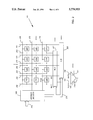
- FIG. 1 is a schematic illustrating a destructive read sense-amp
- FIG. 2 is a schematic illustrating components of a SRAM in general.
- FIG. 3 is a schematic illustrating details of one of the FIG. 2 SRAM memory cells.
- FIG. 4 is a schematic illustrating a conventional SRAM sense-amp.
- a destructive read sense-amp 100 is pictured in FIG. 1, and may generally comprise means 116, 118 for disabling its amplifier circuitry in response to a predetermined logic level appearing at its output 110, means 120 for preserving the predetermined logic level appearing at its output 110, and means 132 for modifying data carried on data transmission lines 104, 106 connected to its differential inputs 134, 136.
- the output preserving means 120 and data modifying means 132 are only enabled while the sense-amp's amplifier circuitry is disabled.
- a destructive read sense-amp 100 may comprise differential inputs 134, 136 connected to data transmission lines 104, 106, an enable input 138, a reference node 108, a plurality of switches (M9, M10, M11, M12, M17), and a number of inverters 112, 122, 126.
- the plurality of switches may comprise first and second numbers of switches (M11, M12), a number of feedback loop switches (M17), and a number of data writing switches (M9, M10).
- the first number of switches may be connected between the sense-amp's enable input 138 and a power rail.
- the second number of switches may be connected between the sense-amp's reference node 108 and a power rail.
- the number of feedback loop switches may be connected between the sense-amp's output 110 and a power rail.
- Each of the number of data writing switches may be connected between a differential input 134, 136 of the sense-amp and a power rail.
- the number of inverters 112, 122, 126 may be connected to the amplifier's output 110 as a serial inverter string 130, and outputs 124, 128 of the number of inverters 112, 122, 126 may be connected to terminals of the first and second numbers of switches, the feedback loop switches, and the data writing switches.
- a method of reading and modifying data 300, 302 (FIG. 3) stored in a static random access memory (SRAM) 200 may comprise the steps of initiating a read of a sense-amp's differential inputs 134, 136, disabling the sense-amp's differential inputs 134, 136 in response to a predetermined logic level appearing at the sense-amp's output 110, preserving the predetermined logic level appearing at the sense-amp's output 110, and modifying data carried on data transmission lines 104, 106 connected to the sense-amp's differential inputs 134, 136.
- the output preserving and data modifying steps are only performed while the sense-amp's differential inputs 134, 136 are disabled.
- An SRAM 200 is a collection of numerous rows of memory cells 202-224, as illustrated in FIG. 2.
- data comprising a single SRAM output bit 110 will be selected from among a grid of many columns 238-252 and rows 230-234 of memory cells 202-224.
- a typical memory cell 206 is illustrated in FIG. 3, and comprises a pair of cross coupled inverters (i.e., transistors 308-314). Positive and negative senses of data are held at nodes D 246 and ND 238 until the ROW 234 comprising the memory cell 206 is addressed, and data flows out of the memory cell 206 on differential bit lines BIT 300 and NBIT 302.
- a memory address 226 is supplied to an SRAM's address decoder 228, a row 234 of cells 206, 212, 218, 224 in the SRAM 200 is activated, and data contained in individual cells 206, 212, 218, 224 is driven to differential bit lines 238-252 (denoted BIT 246 and NBIT 238 with respect to memory cell 206 in FIG. 2).
- Positive 246-252 and negative 238-244 differential data lines are then multiplexed 254, 256 for each bit 114/128 of an SRAM's output, and differential data transmission lines 258, 260 supply the contents of a single SRAM memory cell (i.e., memory cell 206) to a sense-amp 262.
- a sense-amp 400 (FIG. 4) inherently comprises differential inputs 134, 136, an enable input 138, an amplifier (also referred to herein as a "differential amplifier” or “amplifier circuitry”), and an output 110.
- a conventional sense-amp 400 embodying these basic elements is illustrated in FIG. 4, and comprises transistors M1-M8.
- a read cycle begins in the sense-amp 400 as an addressed memory cell 206 (FIGS. 2, 3) drives data 300, 302 to data transmission lines DATA 106 and NDATA 104 (via multiplexed bit lines BIT 246 and NBIT 238), and a READ signal 102 is driven to VDD, thereby causing transistor M1 to conduct current.
- the READ signal 102 Prior to the initiation of a read cycle, the READ signal 102 is held low (i.e., to ground), and transistor M6 pulls the sense-amp's output (NSA -- OUT 110) to VDD (which after an inversion by transistors M7 and M8 produces a low or logic "0" output.
- transistor M1 begins to conduct, amplifier circuitry comprising transistors M2, M3, M4 and M5 is enabled. As a small voltage difference arises between DATA 106 and NDATA 104, transistors M4 and M5 begin to conduct different amounts of current, and in turn, create a difference in potential between reference node N1 108 and the sense-amp's output 110. Since the FIG.
- NSA 13 OUT 110 is inverted again via transistors M7 and M8 (collectively designated as inverter 112) to produce an output (SA 13 OUT 114) which correctly represents the data 300, 302 stored in an addressed memory cell 206.
- transistor M1 (sometimes referred to herein as a "read initiating means") begins to conduct.
- transistor M5 begins to conduct more, causing NSA -- OUT 110 to fall.
- transistor M4 begins to conduct less, causing the voltage at reference node N1 108 to rise.
- transistor M3 (the load transistor for transistor M5) also conducts less, and accelerates the fall of NSA -- OUT 110.
- Transistors M7 and M8 invert and amplify NSA -- OUT 110 producing a rapid voltage rise on SA -- OUT 114. The voltage of SA -- OUT 114 therefore indicates that a logic "1" has just been read from memory.
- a destructive read sense-amp 100 may be constructed by expanding upon the structure of a conventional sense-amp 400.
- the FIG. 1 destructive read sense-amp further comprises transistors M9-M16. These additional transistors form 1) a means 116, 118 for disabling the sense-amp's amplifier circuitry in response to a predetermined logic level appearing at the sense-amp's output 110; 2) a means 120 for preserving the predetermined logic level appearing at the sense-amp's output 110; and 3) a means 132 for modifying data carried on the data transmission lines 104, 106 connected to the sense-amp's differential inputs 134, 136.
- the destructive read sense-amp 100 may therefore set, clear, or otherwise affect stored data 300, 302 in the same cycle in which the stored data 300, 302 is read.
- the means 116, 118 for disabling the sense-amp's amplifier circuitry comprises transistors M11 and M12 (or a number of transistors and/or other components performing substantially the same switching function performed by transistors M11 and M12).
- Transistor M11 is connected between the sense-amp's reference node, N1 108, and a voltage supply.
- Transistor M12 is serially connected to transistor M1 (the sense-amp's read initiating means), and the two transistors are then connected between the sense-amp's enable input 138 and ground.
- a device “connected” between two points may be one of many devices creating an electrical connection between the two points.
- “serially connected” transistors are transistors having a single common source/drain connection.
- the means 120 for preserving the predetermined logic level appearing at the sense-amp's output 110 may comprise a single feedback transistor, M17, connected between the sense-amp's output 110 and ground (or may again comprise a number of transistors and/or other components performing substantially the same switching function performed by transistor M17).
- the means 132 for modifying data carried on the data transmission lines 104, 106 connected to the sense-amp's differential inputs 134, 136 may comprise first and second data modification transistors, M9 and M10, wherein each is connected between a different one of the data transmission lines 104, 106 and a programmed voltage value (e.g., a power rail such as VDD or ground).
- a programmed voltage value e.g., a power rail such as VDD or ground.
- each of the transistors comprising the data modifying means may be replaced with a number of transistors and/or other components (sometimes referred to in the claims as "data writing switches") performing substantially the same switching functions performed by transistors M9 and M10.
- Each of transistors M9-M12 and M17 is driven by an output of a number of inverters 112, 122, 126 connected to the sense-amp's output as a serial inverter string 130.
- the inverter string 130 comprises transistors M13-M16.
- Inverters 122 and 126 assist in driving NOUT 124 and OUT 128 to respective power rails, and provide sharp digital signals for switching the transistors of the amplifier disabling, output preserving, and data modifying means 116, 118, 120, 132.
- the additional inverters 122, 126 also create advantageous timing delays.
- output NOUT 124 is routed to the gate terminals of the transistors comprising the amplifier disabling means 116, 118, while output OUT 128 is routed to the gate terminals of the transistors comprising the output preserving and data modification means 120, 132.
- a destructive read sense-amp 100 may be configured to alter stored data 300, 302 upon a predetermined logic level appearing at the sense-amp's output 110.
- the predetermined logic level is substantially zero volts (i.e., close enough to zero to register a logic "0" at NSA -- OUT 110), and the data written to memory upon the occurence of this predetermined logic level is a logic "0".
- a logic "0" is written to memory when a logic "1" is read from a bit 128 of the SRAM 200 generated by the FIG. 1 sense-amp 100.
- transistor M6 Before a read cycle begins, transistor M6 is pulling NSA -- OUT 110 to VDD. This creates the initial output conditions given below:
- the destructive read sense-amp 100 operates similarly to a conventional sense-amp 400 (i.e., transistors M1-M8 operate in a similar fashion). But consider a read of a logic "1". The logic "1" is read as before. However, as NSA -- OUT 110 falls, SA -- OUT 114 rises, NOUT 124 falls, and OUT 128 rises. When NOUT 124 falls, the differential amplifier is disabled by transistors M11 and M12. In order to retain the logic "11" value that was read, OUT 128 causes transistor M17 to pull NSA -- OUT 110 to GND (thereby creating a feedback loop).
- the data just read may be changed to a logic "0". This occurs when OUT 128 drives the gates of transistors M9 and M10, causing NDATA 104 to be pulled to VDD-V t (where V t is the threshold voltage of transistor M9), and DATA 106 to be pulled to GND.
- the initial output conditions of the destructive read sense-amp 100 are reset as the READ signal 102 falls, and transistor M6 pulls NSA -- OUT 110 to VDD.
- transistor M6 In designing a destructive read sense-amp 100 for a particular use, care should be taken to size transistor M6 larger than transistor M17. In the case where a logic "1" is read, transistor M17 will be pulling NSA -- OUT 110 to GND as the read cycle ends. When the READ signal 102 falls, a drive-fight between transistors M6 and M17 ensues. However, if transistor M6 is larger, NSA -- OUT 110 is pulled above the trip point of the CMOS inverter 112 composed of transistors M7 and M8. This causes SA -- OUT 114 to fall, and the initial output conditions designated above to occur. When OUT 128 falls, transistor M17 turns off and the drive-fight ends.
Landscapes
- Static Random-Access Memory (AREA)
Abstract
Description
______________________________________
       Node    Potential
______________________________________
       NSA.sub.-- OUT
               VDD
       SA.sub.-- OUT
               GND
       NOUT    VDD
       OUT     GND
______________________________________
Claims (20)
Priority Applications (2)
| Application Number | Priority Date | Filing Date | Title |
|---|---|---|---|
| US08/785,188 US5770953A (en) | 1997-01-17 | 1997-01-17 | Destructive read sense-amp |
| JP10002120A JPH10208486A (en) | 1997-01-17 | 1998-01-08 | Destructive reading sense amplifier |
Applications Claiming Priority (1)
| Application Number | Priority Date | Filing Date | Title |
|---|---|---|---|
| US08/785,188 US5770953A (en) | 1997-01-17 | 1997-01-17 | Destructive read sense-amp |
Publications (1)
| Publication Number | Publication Date |
|---|---|
| US5770953A true US5770953A (en) | 1998-06-23 |
Family
ID=25134706
Family Applications (1)
| Application Number | Title | Priority Date | Filing Date |
|---|---|---|---|
| US08/785,188 Expired - Fee Related US5770953A (en) | 1997-01-17 | 1997-01-17 | Destructive read sense-amp |
Country Status (2)
| Country | Link |
|---|---|
| US (1) | US5770953A (en) |
| JP (1) | JPH10208486A (en) |
Cited By (1)
| Publication number | Priority date | Publication date | Assignee | Title |
|---|---|---|---|---|
| US20050267150A1 (en) * | 1998-06-22 | 2005-12-01 | Thompson Richard C | Cycloalkyl, lactam, lactone and related compounds, pharmaceutical compositions comprising same, and methods for inhibiting beta-amyloid peptide release and/or its synthesis by use of such compounds |
Citations (3)
| Publication number | Priority date | Publication date | Assignee | Title |
|---|---|---|---|---|
| US5015891A (en) * | 1988-12-30 | 1991-05-14 | Samsung Electronics Co., Ltd. | Output feedback control circuit for integrated circuit device |
| US5508643A (en) * | 1994-11-16 | 1996-04-16 | Intel Corporation | Bitline level insensitive sense amplifier |
| US5627484A (en) * | 1995-09-08 | 1997-05-06 | International Business Machines Corporation | CMOS sense amplifier |
-
1997
- 1997-01-17 US US08/785,188 patent/US5770953A/en not_active Expired - Fee Related
-
1998
- 1998-01-08 JP JP10002120A patent/JPH10208486A/en active Pending
Patent Citations (3)
| Publication number | Priority date | Publication date | Assignee | Title |
|---|---|---|---|---|
| US5015891A (en) * | 1988-12-30 | 1991-05-14 | Samsung Electronics Co., Ltd. | Output feedback control circuit for integrated circuit device |
| US5508643A (en) * | 1994-11-16 | 1996-04-16 | Intel Corporation | Bitline level insensitive sense amplifier |
| US5627484A (en) * | 1995-09-08 | 1997-05-06 | International Business Machines Corporation | CMOS sense amplifier |
Cited By (1)
| Publication number | Priority date | Publication date | Assignee | Title |
|---|---|---|---|---|
| US20050267150A1 (en) * | 1998-06-22 | 2005-12-01 | Thompson Richard C | Cycloalkyl, lactam, lactone and related compounds, pharmaceutical compositions comprising same, and methods for inhibiting beta-amyloid peptide release and/or its synthesis by use of such compounds |
Also Published As
| Publication number | Publication date |
|---|---|
| JPH10208486A (en) | 1998-08-07 |
Similar Documents
| Publication | Publication Date | Title |
|---|---|---|
| JP4824952B2 (en) | Series wake-up circuit to prevent power noise of memory device | |
| EP0186906B1 (en) | Semiconductor memory attaining high data read speed and having high noise margin | |
| EP1614118B1 (en) | Low-voltage sense amplifier and method | |
| EP0107415B1 (en) | A static memory circuit | |
| JPS59178685A (en) | Semiconductor storage circuit | |
| US11270761B2 (en) | Dual-mode high-bandwidth SRAM with self-timed clock circuit | |
| TW202301334A (en) | Memory device, sense amplifier system and controlling method thereof | |
| US4679172A (en) | Dynamic memory with increased data retention time | |
| US6459611B2 (en) | Low power SRAM memory cell having a single bit line | |
| JP2000021180A (en) | Dynamic sense amplifier provided with built-in latch | |
| US5719812A (en) | Semiconductor memory including bit line reset circuitry and a pulse generator having output delay time dependent on type of transition in an input signal | |
| US7203097B2 (en) | Method of operating a semiconductor device and the semiconductor device | |
| GB2234873A (en) | Four transistor pseudo-static ram cell | |
| KR0127240B1 (en) | A column start signal generating device of storage element | |
| KR100468718B1 (en) | Refresh control circuit and Refresh control method with no external refresh command at memory device | |
| JP2010080054A (en) | Sensing amplifier for nonvolatile ferroelectric memory device | |
| JPH01119982A (en) | Static type random access memory | |
| JP3188634B2 (en) | Data holding circuit | |
| JPS62165785A (en) | Semiconductor memory device | |
| KR0154755B1 (en) | Semiconductor memory device having variable plate voltage generation circuit | |
| US4823322A (en) | Dynamic random access memory device having an improved timing arrangement | |
| US5770953A (en) | Destructive read sense-amp | |
| CN1728278B (en) | Method for operating semiconductor device and semiconductor device | |
| TW202213337A (en) | Boost circuit | |
| JPS5954094A (en) | Semiconductor storage device |
Legal Events
| Date | Code | Title | Description |
|---|---|---|---|
| AS | Assignment |
Owner name: HEWLETT PACKARD COMPANY, CALIFORNIA Free format text: ASSIGNMENT OF ASSIGNORS INTEREST;ASSIGNOR:ELDREDGE, JAMES G.;REEL/FRAME:008540/0523 Effective date: 19970117 |
|
| AS | Assignment |
Owner name: HEWLETT-PACKARD COMPANY, A DELAWARE CORPORATION, C Free format text: MERGER;ASSIGNOR:HEWLETT-PACKARD COMPANY, A CALIFORNIA CORPORATION;REEL/FRAME:010841/0649 Effective date: 19980520 |
|
| AS | Assignment |
Owner name: AGILENT TECHNOLOGIES INC, CALIFORNIA Free format text: ASSIGNMENT OF ASSIGNORS INTEREST;ASSIGNOR:HEWLETT-PACKARD COMPANY;REEL/FRAME:010977/0540 Effective date: 19991101 |
|
| FEPP | Fee payment procedure |
Free format text: PAYOR NUMBER ASSIGNED (ORIGINAL EVENT CODE: ASPN); ENTITY STATUS OF PATENT OWNER: LARGE ENTITY |
|
| FPAY | Fee payment |
Year of fee payment: 4 |
|
| REMI | Maintenance fee reminder mailed | ||
| FPAY | Fee payment |
Year of fee payment: 8 |
|
| AS | Assignment |
Owner name: AVAGO TECHNOLOGIES GENERAL IP PTE. LTD., SINGAPORE Free format text: ASSIGNMENT OF ASSIGNORS INTEREST;ASSIGNOR:AGILENT TECHNOLOGIES, INC.;REEL/FRAME:017207/0020 Effective date: 20051201 |
|
| REMI | Maintenance fee reminder mailed | ||
| LAPS | Lapse for failure to pay maintenance fees | ||
| STCH | Information on status: patent discontinuation |
Free format text: PATENT EXPIRED DUE TO NONPAYMENT OF MAINTENANCE FEES UNDER 37 CFR 1.362 |
|
| FP | Lapsed due to failure to pay maintenance fee |
Effective date: 20100623 |
|
| AS | Assignment |
Owner name: AVAGO TECHNOLOGIES GENERAL IP (SINGAPORE) PTE. LTD., SINGAPORE Free format text: CORRECTIVE ASSIGNMENT TO CORRECT THE NAME OF THE ASSIGNEE PREVIOUSLY RECORDED ON REEL 017207 FRAME 0020. ASSIGNOR(S) HEREBY CONFIRMS THE ASSIGNMENT;ASSIGNOR:AGILENT TECHNOLOGIES, INC.;REEL/FRAME:038633/0001 Effective date: 20051201 Owner name: AVAGO TECHNOLOGIES GENERAL IP (SINGAPORE) PTE. LTD Free format text: CORRECTIVE ASSIGNMENT TO CORRECT THE NAME OF THE ASSIGNEE PREVIOUSLY RECORDED ON REEL 017207 FRAME 0020. ASSIGNOR(S) HEREBY CONFIRMS THE ASSIGNMENT;ASSIGNOR:AGILENT TECHNOLOGIES, INC.;REEL/FRAME:038633/0001 Effective date: 20051201 |