US5767686A - Device for contactless detection of the position of a moving web - Google Patents
Device for contactless detection of the position of a moving web Download PDFInfo
- Publication number
- US5767686A US5767686A US08/622,488 US62248896A US5767686A US 5767686 A US5767686 A US 5767686A US 62248896 A US62248896 A US 62248896A US 5767686 A US5767686 A US 5767686A
- Authority
- US
- United States
- Prior art keywords
- electrode
- strip
- conductive material
- detector
- electrodes
- Prior art date
- Legal status (The legal status is an assumption and is not a legal conclusion. Google has not performed a legal analysis and makes no representation as to the accuracy of the status listed.)
- Expired - Lifetime
Links
- 238000001514 detection method Methods 0.000 title claims abstract description 7
- 230000005540 biological transmission Effects 0.000 claims abstract description 63
- 238000012216 screening Methods 0.000 claims abstract description 30
- 239000004020 conductor Substances 0.000 claims description 70
- 238000011156 evaluation Methods 0.000 claims description 23
- 238000003491 array Methods 0.000 claims description 7
- 230000000694 effects Effects 0.000 claims description 7
- 238000009413 insulation Methods 0.000 claims description 4
- 238000006073 displacement reaction Methods 0.000 abstract description 11
- 230000035945 sensitivity Effects 0.000 abstract description 7
- 230000008878 coupling Effects 0.000 abstract description 5
- 238000010168 coupling process Methods 0.000 abstract description 5
- 238000005859 coupling reaction Methods 0.000 abstract description 5
- 238000005259 measurement Methods 0.000 abstract description 2
- 238000013461 design Methods 0.000 description 7
- 239000012212 insulator Substances 0.000 description 4
- 238000012544 monitoring process Methods 0.000 description 3
- 238000013459 approach Methods 0.000 description 2
- 239000003990 capacitor Substances 0.000 description 2
- 238000002955 isolation Methods 0.000 description 2
- 230000002411 adverse Effects 0.000 description 1
- 238000001035 drying Methods 0.000 description 1
- 238000010438 heat treatment Methods 0.000 description 1
- 239000012535 impurity Substances 0.000 description 1
- 238000009434 installation Methods 0.000 description 1
- 238000012423 maintenance Methods 0.000 description 1
- 238000000034 method Methods 0.000 description 1
- 230000003071 parasitic effect Effects 0.000 description 1
- 230000010363 phase shift Effects 0.000 description 1
- 238000012545 processing Methods 0.000 description 1
- 239000000725 suspension Substances 0.000 description 1
- 238000012546 transfer Methods 0.000 description 1
- 238000003466 welding Methods 0.000 description 1
Images

Classifications
-
- B—PERFORMING OPERATIONS; TRANSPORTING
- B65—CONVEYING; PACKING; STORING; HANDLING THIN OR FILAMENTARY MATERIAL
- B65H—HANDLING THIN OR FILAMENTARY MATERIAL, e.g. SHEETS, WEBS, CABLES
- B65H23/00—Registering, tensioning, smoothing or guiding webs
- B65H23/02—Registering, tensioning, smoothing or guiding webs transversely
- B65H23/0204—Sensing transverse register of web
-
- G—PHYSICS
- G01—MEASURING; TESTING
- G01B—MEASURING LENGTH, THICKNESS OR SIMILAR LINEAR DIMENSIONS; MEASURING ANGLES; MEASURING AREAS; MEASURING IRREGULARITIES OF SURFACES OR CONTOURS
- G01B7/00—Measuring arrangements characterised by the use of electric or magnetic techniques
- G01B7/003—Measuring arrangements characterised by the use of electric or magnetic techniques for measuring position, not involving coordinate determination
-
- G—PHYSICS
- G01—MEASURING; TESTING
- G01D—MEASURING NOT SPECIALLY ADAPTED FOR A SPECIFIC VARIABLE; ARRANGEMENTS FOR MEASURING TWO OR MORE VARIABLES NOT COVERED IN A SINGLE OTHER SUBCLASS; TARIFF METERING APPARATUS; MEASURING OR TESTING NOT OTHERWISE PROVIDED FOR
- G01D5/00—Mechanical means for transferring the output of a sensing member; Means for converting the output of a sensing member to another variable where the form or nature of the sensing member does not constrain the means for converting; Transducers not specially adapted for a specific variable
- G01D5/12—Mechanical means for transferring the output of a sensing member; Means for converting the output of a sensing member to another variable where the form or nature of the sensing member does not constrain the means for converting; Transducers not specially adapted for a specific variable using electric or magnetic means
- G01D5/14—Mechanical means for transferring the output of a sensing member; Means for converting the output of a sensing member to another variable where the form or nature of the sensing member does not constrain the means for converting; Transducers not specially adapted for a specific variable using electric or magnetic means influencing the magnitude of a current or voltage
- G01D5/24—Mechanical means for transferring the output of a sensing member; Means for converting the output of a sensing member to another variable where the form or nature of the sensing member does not constrain the means for converting; Transducers not specially adapted for a specific variable using electric or magnetic means influencing the magnitude of a current or voltage by varying capacitance
- G01D5/2403—Mechanical means for transferring the output of a sensing member; Means for converting the output of a sensing member to another variable where the form or nature of the sensing member does not constrain the means for converting; Transducers not specially adapted for a specific variable using electric or magnetic means influencing the magnitude of a current or voltage by varying capacitance by moving plates, not forming part of the capacitor itself, e.g. shields
Definitions
- the present invention relates to a device for the contactless detection of a moving web, and more particularly, but not by way of limitation, to a device for the contactless detection of a moving web wherein the device has a detector electrode disposed adjacent one side of the web and wherein the detector electrode and the web are maintained at substantially the same voltage potential such that the interference capacitance between the web and the detector electrode is substantially eliminated.
- the present invention concerns a device for the contactless detection of the position of a moving web consisting of conductive material and connected to zero or ground potential, with a width detector electrode on one side of the web, arranged parallel to the web and overlapping the area of the web edges, and a pair of edge electrodes arranged on the other side of the web in the area of its edges opposite the width detector electrode, whereby one of the two electrode arrays forms a transmission electrode array connected to an oscillator and the other a detector electrode array capacitively coupled to the transmission electrode array in such a way that two coupling paths are formed in the area of the two edges of the web and a lateral displacement of the web acts on the two couplings in opposing ways, and whereby an evaluation circuit is connected to the detector electrode array to obtain a position deviation signal to control the web movement.
- a device is known from Patent No. DE-PS 40 09 697.
- the first element in the evaluation circuit for obtaining the position deviation signal is a voltage measurement array with a certain, relatively high-ohmage input resistance, at which the capacitive transfer currents cause a voltage drop, which is amplified by an input amplifier and if necessary led to a demodulator for further processing.
- this known device for detecting the position of a moving web is largely immune to external interference, and is more sensitive to changes of web position than the devices described in DE-OS 27 44 785.
- the devices described above also have the drawback that the sensitivity to changes in the position of the web depends on the width of the web. For certain applications, this makes the measuring device unusable, because with such a device it is impossible to set the control apparatus without knowing the width of the web.
- the dependence of measuring sensitivity on the width of the web is due to the capacitive load on the detector electrode(s) by the web itself. This arises because of the interference capacitance(s) formed by the detector electrode(s) and the web, which varies according to the width of the web. In a design where the width measuring electrode is the detector electrode, this interference makes itself felt where, with the web in a non-central position, an A.C. voltage potential other than zero occurs at the electrode. This A.C. voltage at the detector electrode is loaded with the interference capacitance between the web and the detector electrode, forming a parasitic shunt to the measuring resistor.
- the capacitive displacement current flowing across this capacitance reduces the voltage at the detector electrode, because a capacitive voltage divider is formed between the transmission electrodes, the detector electrode and the web.
- this effect means that the control system responds more slowly and sluggishly with wide webs than is the case with narrow webs.
- the aim of the invention is to improve the device for detecting the position of a moving web of the aforementioned type in such a way that, while retaining the compact design, the insensitivity to external interference and the good sensitivity to changes in web position, there is no change in sensitivity as a function of web width.
- the invention resolves this problem by virtue of the fact that the evaluation circuit forces the potential of the detector electrodes) to remain at zero. This can be achieved in particular by ensuring that the input impedance of the evaluation circuit is very small. The currents discharged via the evaluation circuit then serve to provide the measuring signal. Where a non-linear system is used, the input impedance of the evaluation circuit must be very small, at least for the given signal profile.
- the senor is not sensitive to any approach of the web towards the detector electrode or to any twisting of the web out of the horizontal position.
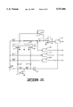
- FIG. 1 is a diagrammatic, partial cross-sectional, schematic view of a sensor device constructed in accordance with the present invention.
- FIG. 2 is a diagrammatic, partial cross-sectional, schematic view of another sensor device constructed in accordance with the present invention.
- FIG. 3 is a diagrammatic, partial cross-sectional, schematic view of the sensor device of FIG. 1 having an additional arrangement for monitoring the insulating effect of the electrode suspension system.
- the arrangement of the electrodes relative to a moving web or grounded strip of conductive material 2 is shown in schematic cross-section, i.e. the web 2 moves into or out of the plane of projection, and is surrounded at a certain distance by the different electrodes.
- transmission electrodes 4 and 5 are arranged below the web 2 in the area of its edges, and are screened by screening electrodes 7 and 8 which are associated with the electrodes 4 and 5 substantially as shown in FIG. 1.
- the transmission electrodes 4 and 5 have portions extending beyond the respective edges of the web 2.
- An oscillator 9 sends a signal to transmission electrode 5 directly, and to transmission electrode 4 via an inverting amplifier 14.
- the inverting amplifier 14 is an operational amplifier which, in conjunction with resistors R1, R2, causes a 180° phase shift in the signal.
- a detector electrode 3 Above the web 2, extending across its entire width and having portions extending beyond the adjacent edge areas, is a detector electrode 3, to which an evaluation circuit means, such as a current-to-voltage converter 10, is connected.
- the current-to-voltage converter 10 comprises an operational amplifier 101 and an impedance Z1 which feeds back the output of the operational amplifier 10 to the inverting input.
- the output of the current-tovoltage converter 10 is sent to a demodulator 15.
- the area of the detector electrode 3 which is turned away from the web 2 is surrounded by a screening electrode 6, which is connected to the output of an isolation amplifier 11, whose input is connected to the detector electrode 3.
- the oscillator 9 feeds the transmission electrode 5 and the inverting amplifier 14.
- the inverting amplifier 14 ensures that the same signal amplitude is present at the transmission electrode 4 as to transmission electrode 5, except that the phase angle of the signal at transmission electrode 4 is shifted through 180° relative to the signal at transmission electrode 5. Under these conditions, no signal will be present at the detector electrode 3 if the web 2 is running centrally through the device, because a capacitive displacement current flows from each of the two transmission electrodes 4 and 5 to the detector electrode 3, and the effects of the two currents are cancelled out at the detector electrode 3.
- the capacitive coupling will become stronger on one edge and weaker on the other.
- the capacitive displacement current from one transmission electrode will prevail over the other transmission electrode, producing a differential current in the detector electrode 3.
- This differential current reaches the negative input of the operational amplifier 101, which is negatively fed back via Z1.
- the non-inverting input of the operational amplifier 101 is connected to ground potential.
- the operational amplifier 101 is designed in such a way that it has a very high input impedance. Under these conditions the differential current of the web centre sensor must for the most part flow through the negative feedback resistor Z1, and the voltage drop at Z1 determines the output voltage U. of the operational amplifier 101.
- phase angle of the output voltage U. indicates which coupling has become stronger and which weaker, and thus the direction of displacement of the web 2.
- a dashed line shows a signal path for the phase angle from the oscillator 9 to the demodulator 15.
- the input voltage U of the operational amplifier 101 is given by
- U is the voltage at the input
- U. is the voltage at the output
- V. is the open-loop voltage gain of the operational amplifier 101. If the operational amplifier 101 is designed in such a way that V. is very large, then the voltage at the input of the operational amplifier 101 and thus also at the detector electrode 3 will be very small, and the current-to-voltage converter 10 will generally exhibit a very low input impedance such that the current-to-voltage converter 10 maintains the detector electrode 3 at substantially the same voltage potential as the web 2 so that the voltage potential on the detector electrode 3 follows the voltage potential on the web 2 whereby interference capacitance between the web 2 and the detector electrode 3 is substantially eliminated.
- the voltage U is the voltage at the input
- U. is the voltage at the output
- V. is the open-loop voltage gain of the operational amplifier 101.
- the A.C. output voltage of the current-to-voltage converter 10 is thus a measure of the position of the web 2 in the device. It can either be used directly or converted by a demodulator 15 into a proportional D.C. voltage.
- the screening electrode 6 serves to prevent interference from the environment, which may be caused by people 1 standing nearby or by asymmetrically arranged, conductive machine parts, and also by interference fields of other devices of the overall installation (welding machines, electrostatic oilers, thyristor-controlled motors etc.). Simple earthing (or grounding) of the screening electrode 6 is not ideal, because total enforcement of zero or ground potential at the detector electrode 6 is impossible in practice.
- the operational amplifier 101 is typically a TL 084 ACD sold by Texas Instruments.
- the impedance Z1 is typically a 3 Mega-Ohm resistor connected in parallel with a 100 pF capacitor.
- the width detector electrode is the transmission electrode 3', which is fed by the oscillator 9' and from which the capacitive displacement currents flow to the two detector electrodes 4', 5', which here constitute the edge electrodes.
- These two displacement currents are now --individually --led to an evaluation circuit with a current-to-voltage converter comprising a first operational amplifier 10'and a second operational amplifier 12', as described for the first design.
- a current-to-voltage converter comprising a first operational amplifier 10'and a second operational amplifier 12', as described for the first design.
- a third operational amplifier or difference amplifier 14' forms the difference between the output signals of the current-to-voltage converters 10', 12', and the signal obtained in this way is again led to the demodulator 15'.
- the difference amplifier 14' is typically an operational amplifier.
- FIG. 3 shows a further design of the first variant in which the insulation of the active electrodes of the device is monitored. Since the individual electrodes have to be fastened to the frame of the device via insulators, conductive impurities on the surface of these insulators can impair the functioning of the device. Particularly where such devices are installed in drying or heating furnaces, such insulation monitoring is particularly advantageous, since it is often very difficult and laborious for maintenance personnel to gain access, and soiling of the insulators may well occur, depending on the furnace atmosphere.
- the three electrodes 4" and 5" are connected to a D.C. voltage source 21" via resistors R3', R4" and R5".
- the D.C. voltage at the electrodes can be monitored by the comparators 18", 19" and 20".
- an alarm signal is obtained at the outputs of the comparators 18", 19” and 20" before the soiling of the insulators impairs the functioning of the device.
- the capacitors C1", C2" and C3" decouple the position signal evaluation from the insulation monitoring.
Landscapes
- Physics & Mathematics (AREA)
- General Physics & Mathematics (AREA)
- Engineering & Computer Science (AREA)
- Power Engineering (AREA)
- Measurement Of Length, Angles, Or The Like Using Electric Or Magnetic Means (AREA)
Abstract
Description
U=-U./V/
Claims (26)
Applications Claiming Priority (2)
| Application Number | Priority Date | Filing Date | Title |
|---|---|---|---|
| DE19511646.1 | 1995-03-30 | ||
| DE19511646A DE19511646C2 (en) | 1995-03-30 | 1995-03-30 | Device for contactless detection of the position of a running material band |
Publications (1)
| Publication Number | Publication Date |
|---|---|
| US5767686A true US5767686A (en) | 1998-06-16 |
Family
ID=7758138
Family Applications (1)
| Application Number | Title | Priority Date | Filing Date |
|---|---|---|---|
| US08/622,488 Expired - Lifetime US5767686A (en) | 1995-03-30 | 1996-03-26 | Device for contactless detection of the position of a moving web |
Country Status (3)
| Country | Link |
|---|---|
| US (1) | US5767686A (en) |
| EP (1) | EP0734986B1 (en) |
| DE (2) | DE19511646C2 (en) |
Cited By (18)
| Publication number | Priority date | Publication date | Assignee | Title |
|---|---|---|---|---|
| WO2000005593A1 (en) * | 1998-07-24 | 2000-02-03 | Life Measurement Instruments, Inc. | Variable dielectric position transducer and method |
| US6025903A (en) * | 1996-12-13 | 2000-02-15 | Noritsu Koki Co., Ltd. | Piece negative feeding apparatus |
| US6142632A (en) * | 1997-03-24 | 2000-11-07 | Sony Corporation | Film position detection apparatus and method and image film projection apparatus |
| US6437583B1 (en) * | 1996-02-14 | 2002-08-20 | Stmicroelectronics, Inc.. | Capacitive distance sensor |
| US6472246B1 (en) | 1998-02-17 | 2002-10-29 | Stmicroelectronics, Inc. | Electrostatic discharge protection for integrated circuit sensor passivation |
| US6486680B1 (en) * | 2000-06-13 | 2002-11-26 | The North American Manufacturing Company | Edge detector |
| US6512381B2 (en) | 1999-12-30 | 2003-01-28 | Stmicroelectronics, Inc. | Enhanced fingerprint detection |
| US6724324B1 (en) * | 2000-08-21 | 2004-04-20 | Delphi Technologies, Inc. | Capacitive proximity sensor |
| US20050089200A1 (en) * | 2002-03-01 | 2005-04-28 | Idex Asa | Sensor module for measuring surfaces |
| US20060030182A1 (en) * | 2004-07-29 | 2006-02-09 | Rf Technologies, Inc. | Patient presence monitoring system and method |
| US20060119369A1 (en) * | 2004-12-03 | 2006-06-08 | Alps Electric Co., Ltd. | Capacity detecting sensor |
| US7239227B1 (en) | 1999-12-30 | 2007-07-03 | Upek, Inc. | Command interface using fingerprint sensor input system |
| US20070257682A1 (en) * | 2003-03-28 | 2007-11-08 | Canon Kabushiki Kaisha | Potential sensor |
| US20090123039A1 (en) * | 2007-11-13 | 2009-05-14 | Upek, Inc. | Pixel Sensing Circuit with Common Mode Cancellation |
| US8554354B1 (en) | 2010-02-12 | 2013-10-08 | The Board Of Regents For Oklahoma State University | Method for adaptive guiding of webs |
| KR20140079801A (en) * | 2011-10-21 | 2014-06-27 | 마이크로칩 테크놀로지 저머니 Ⅱ 게엠베하 운트 콤파니 카게 | Electrode device for capacitive sensor device for position detection |
| US20170147860A1 (en) * | 2014-08-15 | 2017-05-25 | Shenzhen Huiding Technology Co., Ltd. | Processing method and system for fingerprint sensing signal and fingerprint recognition terminal |
| EP2865282B1 (en) | 2013-09-03 | 2018-04-18 | Hauni Maschinenbau GmbH | Assembly and method for checking rod-shaped articles from the tobacco processing industry |
Families Citing this family (3)
| Publication number | Priority date | Publication date | Assignee | Title |
|---|---|---|---|---|
| WO1999028702A1 (en) * | 1997-11-28 | 1999-06-10 | I.E.E. International Electronics & Engineering S.A.R.L. | Capacitive distance measurement using a non-ideal measuring electrode |
| LU90237B1 (en) * | 1998-04-30 | 1999-11-03 | Iee Sarl | Capacitive sensor, e.g. for passenger seat monitoring for control of motor vehicle airbag |
| EP4076958B1 (en) | 2019-12-19 | 2023-10-04 | Roche Diagnostics GmbH | Method and system of producing a plurality of analytical test strips |
Citations (12)
| Publication number | Priority date | Publication date | Assignee | Title |
|---|---|---|---|---|
| US3312892A (en) * | 1964-05-04 | 1967-04-04 | Technology Instr Corp Of Calif | Contactless electrical transducer having moving parts |
| US3323699A (en) * | 1965-10-04 | 1967-06-06 | Allegheny Ludlum Steel | Strip centerline sensor and control |
| US3341774A (en) * | 1962-07-17 | 1967-09-12 | Comm Res Inc | Capacitance detector having a transmitter connected to one plate and a receiver connected to another plate |
| US3812424A (en) * | 1972-09-27 | 1974-05-21 | Ade Corp | Capacitive wire gauge |
| US4322678A (en) * | 1978-10-30 | 1982-03-30 | Capots Larry H | Identification of materials using their complex dielectric response |
| US4719409A (en) * | 1985-10-02 | 1988-01-12 | Mechanical Technology Incorporated | Digital signal output capacitance sensor displacement gauging system |
| US4837500A (en) * | 1988-04-08 | 1989-06-06 | Schut's Im- & Exporthandel B.V. | Capacitive displacement meter or transducer |
| US4893071A (en) * | 1988-05-24 | 1990-01-09 | American Telephone And Telegraph Company, At&T Bell Laboratories | Capacitive incremental position measurement and motion control |
| US4922181A (en) * | 1987-08-06 | 1990-05-01 | Laetus Systems Limited | Apparatus for monitoring the dielectric constant of an article |
| US5134379A (en) * | 1987-10-02 | 1992-07-28 | Detection Systems Pty., Ltd. | Capacitive material presence detecting apparatus |
| US5309110A (en) * | 1992-03-04 | 1994-05-03 | The Perkin Elmer Corporation | Differential dielectric analyzer |
| US5394095A (en) * | 1990-03-27 | 1995-02-28 | Fife Gmbh | Sensor for strip of conductive material |
Family Cites Families (8)
| Publication number | Priority date | Publication date | Assignee | Title |
|---|---|---|---|---|
| GB1183974A (en) * | 1967-06-05 | 1970-03-11 | Allegheny Ludlum Steel | Monitoring the Lateral Disposition of a Moving Strip of Material |
| DE1574292C3 (en) * | 1967-06-05 | 1979-04-12 | Allegheny Ludlum Steel Corp., Pittsburgh, Pa. (V.St.A.) | Device for scanning the position of the side edge of a moving strip of material |
| DE2429109A1 (en) * | 1974-06-18 | 1976-01-08 | Hauni Werke Koerber & Co Kg | Cigarette paper web monitor - has overlapping capacitive electrodes embedded in roller, connected to control cct. |
| DE2744785B2 (en) * | 1977-10-05 | 1981-05-21 | Robert 7995 Neukirch Buck | Electronic proximity switch |
| US4584885A (en) * | 1984-01-20 | 1986-04-29 | Harry E. Aine | Capacitive detector for transducers |
| DE3518187C1 (en) * | 1985-05-21 | 1986-07-31 | Fraunhofer-Gesellschaft zur Förderung der angewandten Forschung e.V., 8000 München | Device for contactless detection of the position of an object, in particular the oscillations of a vibrating object |
| GB9002701D0 (en) * | 1990-02-07 | 1990-04-04 | Atomic Energy Authority Uk | A gauging system |
| GB2295016A (en) * | 1994-11-07 | 1996-05-15 | British Nuclear Fuels Plc | A transducer |
-
1995
- 1995-03-30 DE DE19511646A patent/DE19511646C2/en not_active Revoked
-
1996
- 1996-03-26 EP EP96104765A patent/EP0734986B1/en not_active Expired - Lifetime
- 1996-03-26 DE DE59607473T patent/DE59607473D1/en not_active Expired - Lifetime
- 1996-03-26 US US08/622,488 patent/US5767686A/en not_active Expired - Lifetime
Patent Citations (12)
| Publication number | Priority date | Publication date | Assignee | Title |
|---|---|---|---|---|
| US3341774A (en) * | 1962-07-17 | 1967-09-12 | Comm Res Inc | Capacitance detector having a transmitter connected to one plate and a receiver connected to another plate |
| US3312892A (en) * | 1964-05-04 | 1967-04-04 | Technology Instr Corp Of Calif | Contactless electrical transducer having moving parts |
| US3323699A (en) * | 1965-10-04 | 1967-06-06 | Allegheny Ludlum Steel | Strip centerline sensor and control |
| US3812424A (en) * | 1972-09-27 | 1974-05-21 | Ade Corp | Capacitive wire gauge |
| US4322678A (en) * | 1978-10-30 | 1982-03-30 | Capots Larry H | Identification of materials using their complex dielectric response |
| US4719409A (en) * | 1985-10-02 | 1988-01-12 | Mechanical Technology Incorporated | Digital signal output capacitance sensor displacement gauging system |
| US4922181A (en) * | 1987-08-06 | 1990-05-01 | Laetus Systems Limited | Apparatus for monitoring the dielectric constant of an article |
| US5134379A (en) * | 1987-10-02 | 1992-07-28 | Detection Systems Pty., Ltd. | Capacitive material presence detecting apparatus |
| US4837500A (en) * | 1988-04-08 | 1989-06-06 | Schut's Im- & Exporthandel B.V. | Capacitive displacement meter or transducer |
| US4893071A (en) * | 1988-05-24 | 1990-01-09 | American Telephone And Telegraph Company, At&T Bell Laboratories | Capacitive incremental position measurement and motion control |
| US5394095A (en) * | 1990-03-27 | 1995-02-28 | Fife Gmbh | Sensor for strip of conductive material |
| US5309110A (en) * | 1992-03-04 | 1994-05-03 | The Perkin Elmer Corporation | Differential dielectric analyzer |
Cited By (28)
| Publication number | Priority date | Publication date | Assignee | Title |
|---|---|---|---|---|
| US6437583B1 (en) * | 1996-02-14 | 2002-08-20 | Stmicroelectronics, Inc.. | Capacitive distance sensor |
| US6496021B2 (en) * | 1996-02-14 | 2002-12-17 | Stmicroelectronics, Inc. | Method for making a capacitive distance sensor |
| US6025903A (en) * | 1996-12-13 | 2000-02-15 | Noritsu Koki Co., Ltd. | Piece negative feeding apparatus |
| US6142632A (en) * | 1997-03-24 | 2000-11-07 | Sony Corporation | Film position detection apparatus and method and image film projection apparatus |
| US6610555B1 (en) | 1998-02-17 | 2003-08-26 | Stmicroelectronics, Inc. | Selectively doped electrostatic discharge layer for an integrated circuit sensor |
| US6472246B1 (en) | 1998-02-17 | 2002-10-29 | Stmicroelectronics, Inc. | Electrostatic discharge protection for integrated circuit sensor passivation |
| WO2000005593A1 (en) * | 1998-07-24 | 2000-02-03 | Life Measurement Instruments, Inc. | Variable dielectric position transducer and method |
| US7239227B1 (en) | 1999-12-30 | 2007-07-03 | Upek, Inc. | Command interface using fingerprint sensor input system |
| US6512381B2 (en) | 1999-12-30 | 2003-01-28 | Stmicroelectronics, Inc. | Enhanced fingerprint detection |
| US6486680B1 (en) * | 2000-06-13 | 2002-11-26 | The North American Manufacturing Company | Edge detector |
| US6724324B1 (en) * | 2000-08-21 | 2004-04-20 | Delphi Technologies, Inc. | Capacitive proximity sensor |
| US20050089200A1 (en) * | 2002-03-01 | 2005-04-28 | Idex Asa | Sensor module for measuring surfaces |
| US7239153B2 (en) * | 2002-03-01 | 2007-07-03 | Idex Asa | Sensor module for measuring surfaces |
| US7583086B2 (en) * | 2003-03-28 | 2009-09-01 | Canon Kabushiki Kaisha | Potential sensor |
| US20070257682A1 (en) * | 2003-03-28 | 2007-11-08 | Canon Kabushiki Kaisha | Potential sensor |
| US20060030182A1 (en) * | 2004-07-29 | 2006-02-09 | Rf Technologies, Inc. | Patient presence monitoring system and method |
| US20060119369A1 (en) * | 2004-12-03 | 2006-06-08 | Alps Electric Co., Ltd. | Capacity detecting sensor |
| US8115497B2 (en) | 2007-11-13 | 2012-02-14 | Authentec, Inc. | Pixel sensing circuit with common mode cancellation |
| US20090123039A1 (en) * | 2007-11-13 | 2009-05-14 | Upek, Inc. | Pixel Sensing Circuit with Common Mode Cancellation |
| US8554354B1 (en) | 2010-02-12 | 2013-10-08 | The Board Of Regents For Oklahoma State University | Method for adaptive guiding of webs |
| KR20140079801A (en) * | 2011-10-21 | 2014-06-27 | 마이크로칩 테크놀로지 저머니 Ⅱ 게엠베하 운트 콤파니 카게 | Electrode device for capacitive sensor device for position detection |
| JP2014532981A (en) * | 2011-10-21 | 2014-12-08 | マイクロチップ テクノロジー ジャーマニー ツー ゲーエムベーハー ウント コンパニー カーゲー | Electrode device for capacitive sensor device for position detection |
| US9442534B2 (en) | 2011-10-21 | 2016-09-13 | Microchip Technology Germany Ii Gmbh & Co. Kg | Electrode device for a capacitive sensor device for position detection |
| KR101951353B1 (en) | 2011-10-21 | 2019-02-22 | 마이크로칩 테크놀로지 저머니 게엠베하 | Electrode device for capacitive sensor device for position detection |
| EP2865282B1 (en) | 2013-09-03 | 2018-04-18 | Hauni Maschinenbau GmbH | Assembly and method for checking rod-shaped articles from the tobacco processing industry |
| EP2865282B2 (en) † | 2013-09-03 | 2024-07-24 | Körber Technologies GmbH | Assembly and method for checking rod-shaped articles from the tobacco processing industry |
| US20170147860A1 (en) * | 2014-08-15 | 2017-05-25 | Shenzhen Huiding Technology Co., Ltd. | Processing method and system for fingerprint sensing signal and fingerprint recognition terminal |
| US9940501B2 (en) * | 2014-08-15 | 2018-04-10 | Shenzhen GOODIX Technology Co., Ltd. | Method and system for processing fingerprint sensing signals and fingerprint identification terminal |
Also Published As
| Publication number | Publication date |
|---|---|
| DE19511646C2 (en) | 1999-01-07 |
| EP0734986A3 (en) | 1998-01-21 |
| EP0734986B1 (en) | 2001-08-16 |
| DE59607473D1 (en) | 2001-09-20 |
| EP0734986A2 (en) | 1996-10-02 |
| DE19511646A1 (en) | 1996-10-02 |
Similar Documents
| Publication | Publication Date | Title |
|---|---|---|
| US5767686A (en) | Device for contactless detection of the position of a moving web | |
| US7084643B2 (en) | Capacitive sensor for non-contacting gap and dielectric medium measurement | |
| US6194903B1 (en) | Circuit for acquisition of the capacitance or capacitance change of a capacitive circuit element or component | |
| US5442347A (en) | Double-driven shield capacitive type proximity sensor | |
| US8493053B2 (en) | System and device for measuring voltage in a conductor | |
| US3805150A (en) | Environment immune high precision capacitive gauging system | |
| US20030080755A1 (en) | Proximity sensor and object detecting device | |
| US5175505A (en) | Capacitive sensor for measurement of a fuel wall film, particularly in an intake duct of an internal combustion engine | |
| GB2164450A (en) | Arrangement for detecting spatial inhomogeneities in a dielectric | |
| US5394095A (en) | Sensor for strip of conductive material | |
| US4318042A (en) | Electrometer probe | |
| JP2000048694A (en) | Capacitive proximity sensor | |
| US4006411A (en) | Static capacitance type sensor | |
| US4027238A (en) | Method and apparatus for the moisture measurement of flat structures, especially textile webs | |
| EP0723161B1 (en) | Trouble monitor device for bridge circuit | |
| JP4287130B2 (en) | Capacitance detection circuit and capacitance detection method | |
| KR100341966B1 (en) | Impedance-to-voltage converter and converting method | |
| US4768026A (en) | Yarn break detector for spinning and weaving machines | |
| JPS6244680B2 (en) | ||
| US20150276894A1 (en) | Hall-effect-based magnetic field sensor having an improved output bandwidth | |
| US5168239A (en) | Method and apparatus for adjusting the threshold for determining the thickness of or the number of sheets in a sheet material | |
| JPH0448166B2 (en) | ||
| KR101121769B1 (en) | A circuit for radio frequency energy and a method for sensing power | |
| JP2002157671A (en) | Sensing system | |
| US4789822A (en) | Three-electrode sensor for phase comparison and pulse phase adjusting circuit for use with the sensor |
Legal Events
| Date | Code | Title | Description |
|---|---|---|---|
| AS | Assignment |
Owner name: FIFE GMBH, GERMANY Free format text: ASSIGNMENT OF ASSIGNORS INTEREST;ASSIGNOR:KOSPOHL, PETER;REEL/FRAME:007939/0017 Effective date: 19960318 |
|
| STCF | Information on status: patent grant |
Free format text: PATENTED CASE |
|
| CC | Certificate of correction | ||
| AS | Assignment |
Owner name: FIFE-TIDLAND GMBH, GERMANY Free format text: CORRECTION TO THE ASSIGNEE;ASSIGNOR:FIFE GMBH;REEL/FRAME:012312/0809 Effective date: 19960318 |
|
| FPAY | Fee payment |
Year of fee payment: 4 |
|
| AS | Assignment |
Owner name: FLEET CAPITAL CORPORATION, AS AGENT, WISCONSIN Free format text: SUPPLEMENT TO PATENT, TRADEMARK AND LICENSE MORTGAGE;ASSIGNOR:FIFE CORPORATION;REEL/FRAME:013011/0660 Effective date: 20020326 |
|
| AS | Assignment |
Owner name: FIFE CORPORATION, OKLAHOMA Free format text: RELEASE OF SECURITY AGREEMENT;ASSIGNOR:SPECIAL SITUATIONS INVESTING GROUP, INC. AS ADMINISTRATIVE AGENT FOR FLEET CAPITAL CORPORATION;REEL/FRAME:015642/0215 Effective date: 20041013 |
|
| FPAY | Fee payment |
Year of fee payment: 8 |
|
| FPAY | Fee payment |
Year of fee payment: 12 |