US5751522A - Combined-type thin film magnetic head with inductive magnetic head having low-inductive core - Google Patents
Combined-type thin film magnetic head with inductive magnetic head having low-inductive core Download PDFInfo
- Publication number
- US5751522A US5751522A US08/712,662 US71266296A US5751522A US 5751522 A US5751522 A US 5751522A US 71266296 A US71266296 A US 71266296A US 5751522 A US5751522 A US 5751522A
- Authority
- US
- United States
- Prior art keywords
- layer
- coil
- magnetic head
- lower core
- magnetic
- Prior art date
- Legal status (The legal status is an assumption and is not a legal conclusion. Google has not performed a legal analysis and makes no representation as to the accuracy of the status listed.)
- Expired - Lifetime
Links
Images


Classifications
-
- G—PHYSICS
- G11—INFORMATION STORAGE
- G11B—INFORMATION STORAGE BASED ON RELATIVE MOVEMENT BETWEEN RECORD CARRIER AND TRANSDUCER
- G11B5/00—Recording by magnetisation or demagnetisation of a record carrier; Reproducing by magnetic means; Record carriers therefor
- G11B5/127—Structure or manufacture of heads, e.g. inductive
- G11B5/31—Structure or manufacture of heads, e.g. inductive using thin films
- G11B5/3109—Details
- G11B5/312—Details for reducing flux leakage between the electrical coil layers and the magnetic cores or poles or between the magnetic cores or poles
-
- G—PHYSICS
- G11—INFORMATION STORAGE
- G11B—INFORMATION STORAGE BASED ON RELATIVE MOVEMENT BETWEEN RECORD CARRIER AND TRANSDUCER
- G11B5/00—Recording by magnetisation or demagnetisation of a record carrier; Reproducing by magnetic means; Record carriers therefor
- G11B5/127—Structure or manufacture of heads, e.g. inductive
- G11B5/33—Structure or manufacture of flux-sensitive heads, i.e. for reproduction only; Combination of such heads with means for recording or erasing only
- G11B5/39—Structure or manufacture of flux-sensitive heads, i.e. for reproduction only; Combination of such heads with means for recording or erasing only using magneto-resistive devices or effects
- G11B5/3903—Structure or manufacture of flux-sensitive heads, i.e. for reproduction only; Combination of such heads with means for recording or erasing only using magneto-resistive devices or effects using magnetic thin film layers or their effects, the films being part of integrated structures
- G11B5/3967—Composite structural arrangements of transducers, e.g. inductive write and magnetoresistive read
Definitions
- This invention relates to a thin film magnetic head for use as a floating magnetic head, and more particularly to a combined-type thin film magnetic head in which a reproducing head portion having a magnetoresistive device and an inductive magnetic head having a coil layer and a core layer are laminated.
- FIG. 7 illustrates a floating magnetic head H for a hard disk serving as an example of the combined-type thin film magnetic head.
- a slider 1 of the magnetic head H consists of side A serving as a leading side that faces the upstream portion in the direction in which the disk surface is moved and side B serving as a trailing side.
- the surface of the slider 1 that faces the disk has rail-shape surfaces 1a and 1b made of ABS and an air group 1c.
- a combined-type thin film magnetic head 2 is formed on a trailing end surface 1d of the slider 1.
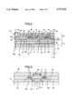
- FIG. 8 is an enlarged cross sectional view taken along line VIII--VIII shown in FIG. 7 and illustrating a laminated structure of the combined-type thin film magnetic head 2.
- FIG. 9 is a partially enlarged front view taken in a direction designated by an arrow IX shown in FIG. 8.
- FIG. 10 is a plan view taken in a direction designated by an arrow X shown in FIG. 8.
- the combined-type thin film magnetic head 2 has a structure in which a reproducing head portion h1 including a magnetoresistive device (an MR device) 12 and an inductive magnetic head h2 are laminated.
- a reproducing head portion h1 including a magnetoresistive device (an MR device) 12 and an inductive magnetic head h2 are laminated.
- the reproducing head portion h1 has, as shown in FIG. 9, a lower shield layer 3 on the trailing end surface of the slider 1, the lower shield layer 3 being a Permalloy (NiFe) layer manufactured by, for example, plating.
- a non-magnetic lower gap layer 11 is formed on the surface of the lower shield layer 3.
- a magnetoresistive device (a MR device) 12 is stacked on the lower gap layer 11.
- the MR device 12 consists of three layers consisting of, when viewed from a lower portion, a SAL film 12a, a non-magnetic SHUNT film 12b and an MR film 12c having a magnetoresistive effect.
- An electrode layer 13 is formed from the two top corners of the MR device 12 to the surface of the lower gap layer 11.
- the electrode layer 13 consists of a lower antiferromagnetic layer (hereinafter called an "AF layer") 13a and an upper electroconductive layer 13b mainly made of tungsten (W).
- the surfaces of the electrode layers 13 are covered with an upper gap layer 15 made of alumina or the like.
- the reproducing head portion h1 has a gap length (G1) that is determined in accordance with the distance from the MR film 12c to the lower shield film 3 or the upper shield layer 4.
- the track width Tw is determined in accordance with a range in which a sense electric current flows through the MR film 12c between the two electrode layers 13.
- leading layers 16 obtained by etching from the same Permalloy plated layer together with the upper shield layer 4 is formed on the surface of the upper gap layer 15.
- the electrode layers 13 extend to the positions at which they overlap with the leading layers 16.
- the electrode layers 13 and the leading layers 16 are electrically connected through contact holes 15a formed in the upper gap layer 15.
- the upper shield layer 4 is also used as a lower core layer.
- An upper core layer 5 formed into a flat shape as shown in FIG. 10 is formed on the surface of the upper shield layer 4.
- a coil layer 6 is formed which has a flat and spiral shape, the center of which is substantially a connection portion 5a between the upper shield layer 4 and the upper core layer 5.
- the upper core layer 5 and the coil layer 6 are covered with an insulating layer and a protective film 7.
- the upper shield layer 4 of the reproducing head portion h1 is also used as the lower core layer of the inductive magnetic head h2 formed on the reproducing head portion h1.
- the upper shield layer 4 also serving as the core has a wide area to enable the coil layer 6 to be formed thereon.
- the coil layer 6 can be, by etching, formed on the smooth surface having no steps.
- the wide area of the upper shield layer 4 also serving as the core causes the cross sectional area of the magnetic passage in the upper shield layer 4 to be enlarged.
- the inductance of a magnetic circuit consisting of the upper shield layer 4, the upper core layer 5 and the coil layer 6 is in proportion to the cross sectional area of the magnetic passage, the conventional combined-type thin film magnetic head suffers from a large inductance of the magnetic circuit thereof. If the inductance is too large, the resonant frequency of the magnetic circuit is lowered and an efficiency of recording high frequency signals deteriorates. Thus, data cannot be recorded on a recording medium at a satisfactory high density.
- the present invention is intended to overcome the problems experienced with the conventional structures and an object of the same is to provide a combined-type thin film magnetic head which is capable of lowering the inductance of a magnetic circuit of an inductive magnetic head and facilitating forming of the coil layer into a flat shape.
- a combined-type thin film magnetic head in which a reproducing head portion that includes a magnetoresistive device and an inductive magnetic head are laminated, wherein the inductive magnetic head has a magnetic material layer having the area that enables a coil layer to be formed, a portion of the magnetic material layer is separated so that a lower core layer is formed, an upper core layer connected to the upper surface of the lower core layer and extending to an upper position of the coil layer is formed, and a magnetic gap is formed between the lower core layer and the upper core layer.
- the magnetic material layer and the lower core layer formed by separating a portion of the magnetic material layer can be used as shield layers to be formed on the gap layer of the reproducing head portion.
- the inductive magnetic head according to the present invention comprises the lower core layer formed by separating a portion of the magnetic material layer that has the area which enables a coil layer to be formed.
- the planar shape of the lower core layer can be reduced and therefore the cross sectional area of the magnetic passage can be reduced. Therefore, the inductance of a magnetic circuit consisting of the lower core layer, the upper core layer and the coil layer can be lowered.
- the recording efficiency can be improved and high density recording can be enabled. Since the coil layer is formed on the magnetic material layer and the lower core layer having sufficiently large areas, generation of a step or the like in the region in which the coil layer will be formed can be prevented. Therefore, the coil layer can be formed precisely on a flat surface similarly to the conventional structure.
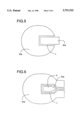
- FIG. 1 is a plan view which illustrates an embodiment of a combined-type thin film magnetic head according to the present invention
- FIG. 2 is a cross sectional view of the combined-type thin film magnetic head shown in FIG. 1 and taken along line II--II of FIG. 1;
- FIG. 3 is a cross sectional view of the combined-type thin film magnetic head shown in FIG. 1 and taken along line III--III of FIG. 1;
- FIGS. 4 (A) to 4 (F) are cross sectional views which illustrate steps of a frame plating method for forming a coil support portion and a lower core portion;
- FIG. 5 is a plan view which illustrates the shapes of the lower core portion and a coil support portion shown in FIG. 1;
- FIG. 6 is a plan view which illustrates other shapes of the lower core portion and a coil support portion
- FIG. 7 is a perspective view which illustrates a floating magnetic head as an applicable example of the combined-type thin film magnetic head
- FIG. 8 is an enlarged cross sectional view taken along line VIII--VIII and illustrating the structure of a conventional combined-type thin film magnetic head
- FIG. 9 is an enlarged front view taken in a direction of an arrow IX shown in FIG. 8.
- FIG. 10 is a plan view taken in a direction of an arrow X shown in FIG. 8.
- FIG. 1 is plan view which illustrates a combined-type thin film magnetic head formed on a trailing-directional-end surface 1d of a slider 1 of a floating magnetic head as shown in FIG. 7.
- FIG. 2 is an enlarged cross sectional view taken along line II--II shown in FIG. 1.
- FIG. 3 is an enlarged cross sectional view taken along line III--III shown in FIG. 1.
- the combined-type thin film magnetic head has a structure in which a reproducing head portion h1 and a recording inductive magnetic head h2 are laminated.
- a lower shield layer 3 is, by plating Permalloy (NiFe), formed on the trailing-directional end surface 1d of the slider 1.
- An alumina (Al 2 O 3 ) lower gap layer 11 is formed on the lower shield layer 3.
- an MR device 12 is formed on the lower gap layer 11.
- the MR device 12 has laminated three layers consisting of, from a lower portion, a SAL film 12a, a SHUNT film 12b and an MR film 12c.
- Electrode layers 13 are formed from the two top corners of the MR device 12 to the top surface of the lower gap layer 11.
- Each of the electrode layers 13 is formed by stacking an AF layer mainly made of FeMn and an electroconductive layer mainly made of tungsten (W).
- the layers of the electrode layer 13 consist of, from a lower portion, NiFe/FeMn/Ta/W/Ta.
- the NiFe and Ta layers are layers for hermetically holding other layers.
- An upper gap layer 15 made of alumina is formed on the MR device 12 and the electrode layers 13.
- a magnetic material layer 21 is formed on the surface of the upper gap layer 15 by electrolytic plating Permalloy (NiFe).
- Permalloy NiFe
- the following Permalloy layers can be formed: lower core portion 21a, coil support portion 21b, leading layers 21c, and terminal raising layers 21d and 21e.
- the coil support portion 21b has a substantially elliptic plane shape. A portion of the coil support portion 21b is separated by a narrow gap ⁇ so that a narrow and elongated lower core portion 21a is formed.
- the lower core portion 21a is formed to cover the portion above the MR device 12. That is, the lower core portion 21a and the coil support portion 21b are also used as upper shield layers formed on the upper gap layer 15 of the reproducing head portion h1.
- the leading layers 21c are formed apart from the two horizontal ends of the coil support portion 21b.
- the electrode layers 13 extend to positions below the leading layers 21c.
- Contact holes 15a are formed in the upper gap layer 15 between the electrode layers 13 and the leading layers 21c. The electrode layers 13 and the leading layers 21c are electrically connected through the contact holes 15a.
- an organic insulating layer 22 made of a resist film or the like is formed between the coil support portion 21b and the terminal raising layers 21d and 21e and between the coil support portion 21b and the leading layers 21c.
- an organic insulating layer 23 made of a resist film is formed on the coil support portion 21b and the lower core layer 21a.
- the surface of the organic insulating layer 23 is a smooth surface for forming a coil layer.
- its organic insulating material is injected into the narrow gap ⁇ having a U-shape facing side and formed between the coil support portion 21b and the lower core portion 21a. Since the gap ⁇ is a small gap, the introduction of the organic insulating material into the gap ⁇ does not deteriorate the smoothness of the surface of the organic insulating layer 23.
- the following method may be employed which comprises the steps of: initially forming the organic insulating layer 22 in the gap ⁇ ; making the surfaces of the coil support layer 21b, the lower core portion 21a and the gap ⁇ to be the same plane; and forming the organic insulating layer 23 on the foregoing plane.
- a coil layer 6 is formed on the smoothed organic insulating layer 23.
- the coil layer 6 is formed such that a copper (Cu) layer having a predetermined thickness is formed on the organic insulating layer 23 and then etching is performed to have a spiral shape.
- a lead layer 6b (see FIG. 1) is continuously and integrally formed with the outermost coil layer 6, the lead layer 6b being the same Cu layer which forms the coil layer 6.
- the leading layer 6b is stacked on the terminal raising layer 21e. Note that the illustrated coil layer 6 has concentric and elliptic annuli shape for the purpose of simplifying the illustration.
- an electrode layer 24 is formed on the terminal raising layer 21d by etching the same Cu layer.
- an organic insulating layer 25 is formed on the coil layer 6. Furthermore, an upper core layer 5 is formed on the organic insulating layer 25 at a position above the lower core portion 21a.
- the upper core layer 5 is formed by plating Permalloy.
- a base portion 5a of the upper core layer 5 is electrically connected to the surface of the lower core portion 21a through a contact hole formed in the organic insulating layers 23 and 25.
- a gap layer 26 made of Al 2 O 3 or SiO 2 is formed between a leading portion 5b of the upper core layer 5 and the lower core portion 21a so that a recording magnetic gap G of the inductive magnetic head h2 is formed.
- a lead layer 27 is formed between a central end 6a of the coil layer 6 and the electrode layer 24 on the terminal raising layer 21d by etching the Permalloy plated layer.
- an insulating layer 28 is formed on the upper core layer 5 and the lead layer 27. Furthermore, a protective film 29 made of alumina is formed on the insulating layer 28. A bump 31 is, by plating, formed on a leading portion 27a of the lead layer 27, the bump 31 electrically connecting a terminal 32 formed on the surface of the protective film 29 and the lead layer 27 to each other.
- the magnetic circuit of the inductive magnetic head is formed by the lower core portion 21a, the upper core layer 5 and the coil layer 6 in such a manner that the lower core portion 21a is formed into an elongated shape that enables the cross sectional area of the magnetic passage to be reduced. Therefore, the inductance of the magnetic circuit can be reduced as compared with the conventional structure. As a result, the resonant frequency of the magnetic circuit can be raised; the recording efficiency can be improved; and a high density recording can be performed.
- the coil support portion 21b and the lower core portion 21a which is separated from the coil support portion 21b gap ⁇ and formed from the same magnetic material layer 21 are formed under the region in which the coil layer 6 is formed, the coil support portion 21b and the lower core portion 21a having the same thickness. Since the width of the gap ⁇ is narrow enough, the organic insulating layer 23 to be formed on the coil support portion 21b and the lower core portion 21a can be formed into a smooth layer. Therefore, the coil layer 6 can precisely be formed on the flat surface.
- the lower core portion 21a and the coil support portion 21b that are separated from each other by the small gap ⁇ as described above can be formed by the frame plating method arranged, for example, as shown in FIG. 4.
- FIG. 4 illustrates, on the same cross section as that shown in FIG. 3, a process for forming the lower core portion 21a and the coil support portion 21b.
- the frame plating method is, in this embodiment, performed in such a manner that a thin base film 35 made of Permalloy or the like is initially formed on the surface of the upper gap layer 15 by sputtering or the like as shown in FIG. 4 (A).
- a resist film R1 is formed on the base film 35 by patterning.
- the Permalloy (magnetic material) layer 21 is formed on the surface of the base film 35 in a region in which the resist film R1 is not formed. Then, the resist film R2 is removed, thus resulting in that the magnetic material layer 21 separated by gaps ⁇ and ⁇ as shown in FIG. 4 (B) can be formed.
- a cover resist film R2 is formed on the magnetic material layer 21 in a region that forms the outlines of the lower core portion 21a and the coil support portion 21b as shown in FIG. 4 (C).
- a cover resist film R2 is injected into the gaps ⁇ and ⁇ .
- the outer plated layer of the lower core portion 21a and the coil support portion 21b is removed by etching as shown in FIG. 4 (D).
- leading layers 21c and terminal raising layers 21d and 21e are formed from the same Permalloy plated layer 21.
- the organic insulating layer 22 is formed around the magnetic material layer 21b and the lower core layer 21a as shown in FIG. 4 (F). Furthermore, the organic insulating layer 23 is formed on the surfaces of the lower core portion 21a and the coil support portion 21b. Simultaneously, the organic insulating material is injected into the gaps ⁇ . Subsequently the coil layer 6 is formed on the smoothed organic insulating layer 23 as described above.
- the shape of the lower core portion 21a is not limited to the elongated shape while being permitted to be formed into an arbitrary shape by patterning the resist film R1.
- the lower core portion 21a may be formed into a shape having a narrow leading portion as shown in FIG. 6.
- the cross sectional area of the magnetic passage in the gap portion can be further reduced. Therefore, the inductance can be lowered furthermore.
- the foregoing embodiment has the arrangement that the lower core portion 21a and the coil support portion 21b made of the Permalloy plated layer 21 also serve as the upper shield layers for the reproducing head portion h1
- another arrangement may be employed in which an upper shield layer having a predetermined area is individually formed on the upper gap layer 15 of the reproducing head portion h1
- the lower core portion 21a and the coil support portion 21b are formed on the upper shield layer on the two sides of the insulating layer
- the coil layer 6 and the upper core layer 5 are formed on the lower core portion 21a and the coil support portion 21b.
- the arrangement that the lower core portion is separated from the coil support portion having the area for forming the coil layer enables the cross sectional area of the magnetic passage in the lower core portion to be reduced. Therefore, the inductance of the magnetic circuit of the inductive magnetic head consisting of the lower core portion, the upper core layer and the coil layer can be lowered. Thus, the recording efficiency can be improved. Since the coil layer is formed on the coil support portion and the lower core portion having predetermined areas, the coil layer can be formed on a region having no step.
- the coil support portion and the lower core portion of the inductive magnetic head are also used as the shield layers for the reproducing head portion, the number of layers required to form the combined-type thin film magnetic head can be decreased. Consequently, a thin magnetic head can be obtained.
Abstract
Description
Claims (1)
Priority Applications (1)
| Application Number | Priority Date | Filing Date | Title |
|---|---|---|---|
| US08/712,662 US5751522A (en) | 1993-10-21 | 1996-09-13 | Combined-type thin film magnetic head with inductive magnetic head having low-inductive core |
Applications Claiming Priority (4)
| Application Number | Priority Date | Filing Date | Title |
|---|---|---|---|
| JP5-285513 | 1993-10-21 | ||
| JP5285513A JP2854513B2 (en) | 1993-10-21 | 1993-10-21 | Composite thin-film magnetic head and method of manufacturing the same |
| US32442994A | 1994-10-17 | 1994-10-17 | |
| US08/712,662 US5751522A (en) | 1993-10-21 | 1996-09-13 | Combined-type thin film magnetic head with inductive magnetic head having low-inductive core |
Related Parent Applications (1)
| Application Number | Title | Priority Date | Filing Date |
|---|---|---|---|
| US32442994A Continuation | 1993-10-21 | 1994-10-17 |
Publications (1)
| Publication Number | Publication Date |
|---|---|
| US5751522A true US5751522A (en) | 1998-05-12 |
Family
ID=17692505
Family Applications (1)
| Application Number | Title | Priority Date | Filing Date |
|---|---|---|---|
| US08/712,662 Expired - Lifetime US5751522A (en) | 1993-10-21 | 1996-09-13 | Combined-type thin film magnetic head with inductive magnetic head having low-inductive core |
Country Status (2)
| Country | Link |
|---|---|
| US (1) | US5751522A (en) |
| JP (1) | JP2854513B2 (en) |
Cited By (23)
| Publication number | Priority date | Publication date | Assignee | Title |
|---|---|---|---|---|
| US5894388A (en) * | 1996-09-10 | 1999-04-13 | Alps Electric Co., Ltd. | Combination read/write thin film magnetic head |
| US5907459A (en) * | 1996-05-23 | 1999-05-25 | Yamaha Corporation | Magnetoresistive thin film magnetic head with specific shapes of leads |
| US5923506A (en) * | 1997-10-03 | 1999-07-13 | Storage Technology Corporation | Recording head element with improved coil tap and method for manufacturing same |
| US5959813A (en) * | 1996-11-19 | 1999-09-28 | Alps Electric Co., Ltd. | Combination read/write thin film magnetic head using a shielding magnetic layer |
| US6178070B1 (en) | 1999-02-11 | 2001-01-23 | Read-Rite Corporation | Magnetic write head and method for making same |
| US6274256B1 (en) | 1998-02-03 | 2001-08-14 | Alps Electric Co., Ltd. | Thin film magnetic head |
| US6278590B1 (en) * | 1998-12-02 | 2001-08-21 | International Business Machines Corporation | High moment laminated layer with nickel cobalt or nickel iron cobalt based alloy layer for first pole piece of write head |
| US6349021B1 (en) | 1999-01-18 | 2002-02-19 | Alps Electric Co., Ltd. | Thin film magnetic head |
| US6392852B1 (en) * | 1999-04-27 | 2002-05-21 | Tdk Corporation | Thin-film magnetic head and method of manufacturing same, and magnetoresistive device |
| US6417998B1 (en) * | 1999-03-23 | 2002-07-09 | Read-Rite Corporation | Ultra small advanced write transducer and method for making same |
| US6462915B1 (en) * | 1998-10-01 | 2002-10-08 | Tdk Corporation | System and method for manufacturing a composite type thin film magnetic head having a reading magnetoresistive effective type thin film magnetic head and a writing inductive type thin film magnetic head that are stacked |
| US6477018B1 (en) * | 1998-07-14 | 2002-11-05 | Tdk Corporation | Thin-film magnetic head and method of manufacturing the same |
| US6560864B1 (en) | 2001-11-14 | 2003-05-13 | Headway Technologies, Inc. | Process for manufacturing a flat coil |
| US6563674B1 (en) | 1998-12-24 | 2003-05-13 | Alps Electric Co., Ltd. | Thin-film magnetic head |
| US6674610B1 (en) * | 2000-06-16 | 2004-01-06 | Western Digital (Fremont), Inc. | Thin film write head with universal coil design |
| GB2391104A (en) * | 2002-07-22 | 2004-01-28 | Alps Electric Co Ltd | Thin film magnetic head |
| US6697234B2 (en) | 1999-05-11 | 2004-02-24 | Alps Electric Co., Ltd. | Thin-film magnetic head having a shielding layer covered by a high-melting point layer on the magnetoresistive element side |
| US20040051998A1 (en) * | 1999-01-13 | 2004-03-18 | Kiyoshi Sato | Thin film magnetic head |
| US6829819B1 (en) | 1999-05-03 | 2004-12-14 | Western Digital (Fremont), Inc. | Method of forming a magnetoresistive device |
| US20050024380A1 (en) * | 2003-07-28 | 2005-02-03 | Lin Lin | Method for reducing random access memory of IC in display devices |
| US20050083606A1 (en) * | 2003-10-15 | 2005-04-21 | Hitachi Global Storage Technologies | Write head design with improved bump to control write saturation |
| US6944938B1 (en) | 1999-05-03 | 2005-09-20 | Western Digital (Fremont), Inc. | Method of forming a magnetoresistive device |
| US8102236B1 (en) | 2010-12-14 | 2012-01-24 | International Business Machines Corporation | Thin film inductor with integrated gaps |
Families Citing this family (5)
| Publication number | Priority date | Publication date | Assignee | Title |
|---|---|---|---|---|
| US5486968A (en) * | 1993-11-10 | 1996-01-23 | International Business Machines Corporation | Method and apparatus for simultaneous write head planarization and lead routing |
| SG34292A1 (en) * | 1994-12-30 | 1996-12-06 | Ibm | Read/write magnetoresistive (MR) head with sunken components |
| JPH0983039A (en) * | 1995-09-14 | 1997-03-28 | Nec Corp | Magnetoresistive effect element |
| US5694276A (en) * | 1996-07-01 | 1997-12-02 | Read-Rite Corporation | Shielded magnetic head having an inductive coil with low mutual inductance |
| WO2002063614A1 (en) * | 2001-02-05 | 2002-08-15 | Fujitsu Limited | Thin film magnetic head, magnetic head assembly, and composite thin film magnetic head |
Citations (9)
| Publication number | Priority date | Publication date | Assignee | Title |
|---|---|---|---|---|
| US3908194A (en) * | 1974-08-19 | 1975-09-23 | Ibm | Integrated magnetoresistive read, inductive write, batch fabricated magnetic head |
| US3975772A (en) * | 1975-06-02 | 1976-08-17 | International Business Machines Corporation | Double shielded magnetorestive sensing element |
| US4841398A (en) * | 1987-02-17 | 1989-06-20 | Magnetic Peripherals Inc. | Non linear magnetoresistive sensor |
| US4907113A (en) * | 1987-07-29 | 1990-03-06 | Digital Equipment Corporation | Three-pole magnetic recording head |
| US4967298A (en) * | 1987-02-17 | 1990-10-30 | Mowry Greg S | Magnetic head with magnetoresistive sensor, inductive write head, and shield |
| US5208715A (en) * | 1990-08-31 | 1993-05-04 | Seagate Technology, Inc. | Shield geometry for stabilizing magnetic domain structure in a magnetoresistive head |
| US5212609A (en) * | 1990-11-19 | 1993-05-18 | Hitachi, Ltd. | Magnetoresistive head |
| US5255141A (en) * | 1991-12-16 | 1993-10-19 | Read-Rite Corp. | Read-write magnetic head with flux sensing read element |
| US5438747A (en) * | 1994-03-09 | 1995-08-08 | International Business Machines Corporation | Method of making a thin film merged MR head with aligned pole tips |
-
1993
- 1993-10-21 JP JP5285513A patent/JP2854513B2/en not_active Expired - Fee Related
-
1996
- 1996-09-13 US US08/712,662 patent/US5751522A/en not_active Expired - Lifetime
Patent Citations (9)
| Publication number | Priority date | Publication date | Assignee | Title |
|---|---|---|---|---|
| US3908194A (en) * | 1974-08-19 | 1975-09-23 | Ibm | Integrated magnetoresistive read, inductive write, batch fabricated magnetic head |
| US3975772A (en) * | 1975-06-02 | 1976-08-17 | International Business Machines Corporation | Double shielded magnetorestive sensing element |
| US4841398A (en) * | 1987-02-17 | 1989-06-20 | Magnetic Peripherals Inc. | Non linear magnetoresistive sensor |
| US4967298A (en) * | 1987-02-17 | 1990-10-30 | Mowry Greg S | Magnetic head with magnetoresistive sensor, inductive write head, and shield |
| US4907113A (en) * | 1987-07-29 | 1990-03-06 | Digital Equipment Corporation | Three-pole magnetic recording head |
| US5208715A (en) * | 1990-08-31 | 1993-05-04 | Seagate Technology, Inc. | Shield geometry for stabilizing magnetic domain structure in a magnetoresistive head |
| US5212609A (en) * | 1990-11-19 | 1993-05-18 | Hitachi, Ltd. | Magnetoresistive head |
| US5255141A (en) * | 1991-12-16 | 1993-10-19 | Read-Rite Corp. | Read-write magnetic head with flux sensing read element |
| US5438747A (en) * | 1994-03-09 | 1995-08-08 | International Business Machines Corporation | Method of making a thin film merged MR head with aligned pole tips |
Cited By (28)
| Publication number | Priority date | Publication date | Assignee | Title |
|---|---|---|---|---|
| US5907459A (en) * | 1996-05-23 | 1999-05-25 | Yamaha Corporation | Magnetoresistive thin film magnetic head with specific shapes of leads |
| US5894388A (en) * | 1996-09-10 | 1999-04-13 | Alps Electric Co., Ltd. | Combination read/write thin film magnetic head |
| US5959813A (en) * | 1996-11-19 | 1999-09-28 | Alps Electric Co., Ltd. | Combination read/write thin film magnetic head using a shielding magnetic layer |
| US5923506A (en) * | 1997-10-03 | 1999-07-13 | Storage Technology Corporation | Recording head element with improved coil tap and method for manufacturing same |
| US6274256B1 (en) | 1998-02-03 | 2001-08-14 | Alps Electric Co., Ltd. | Thin film magnetic head |
| US6477018B1 (en) * | 1998-07-14 | 2002-11-05 | Tdk Corporation | Thin-film magnetic head and method of manufacturing the same |
| US6462915B1 (en) * | 1998-10-01 | 2002-10-08 | Tdk Corporation | System and method for manufacturing a composite type thin film magnetic head having a reading magnetoresistive effective type thin film magnetic head and a writing inductive type thin film magnetic head that are stacked |
| US6278590B1 (en) * | 1998-12-02 | 2001-08-21 | International Business Machines Corporation | High moment laminated layer with nickel cobalt or nickel iron cobalt based alloy layer for first pole piece of write head |
| US6563674B1 (en) | 1998-12-24 | 2003-05-13 | Alps Electric Co., Ltd. | Thin-film magnetic head |
| US6757133B1 (en) | 1999-01-13 | 2004-06-29 | Alps Electric Co., Ltd. | Thin Film magnetic head |
| US6941643B2 (en) | 1999-01-13 | 2005-09-13 | Alps Electric Co., Ltd. | Method of producing a thin film magnetic head |
| US20040051998A1 (en) * | 1999-01-13 | 2004-03-18 | Kiyoshi Sato | Thin film magnetic head |
| US6349021B1 (en) | 1999-01-18 | 2002-02-19 | Alps Electric Co., Ltd. | Thin film magnetic head |
| US6178070B1 (en) | 1999-02-11 | 2001-01-23 | Read-Rite Corporation | Magnetic write head and method for making same |
| US6417998B1 (en) * | 1999-03-23 | 2002-07-09 | Read-Rite Corporation | Ultra small advanced write transducer and method for making same |
| US6392852B1 (en) * | 1999-04-27 | 2002-05-21 | Tdk Corporation | Thin-film magnetic head and method of manufacturing same, and magnetoresistive device |
| US6944938B1 (en) | 1999-05-03 | 2005-09-20 | Western Digital (Fremont), Inc. | Method of forming a magnetoresistive device |
| US6829819B1 (en) | 1999-05-03 | 2004-12-14 | Western Digital (Fremont), Inc. | Method of forming a magnetoresistive device |
| US6697234B2 (en) | 1999-05-11 | 2004-02-24 | Alps Electric Co., Ltd. | Thin-film magnetic head having a shielding layer covered by a high-melting point layer on the magnetoresistive element side |
| US6674610B1 (en) * | 2000-06-16 | 2004-01-06 | Western Digital (Fremont), Inc. | Thin film write head with universal coil design |
| US6560864B1 (en) | 2001-11-14 | 2003-05-13 | Headway Technologies, Inc. | Process for manufacturing a flat coil |
| GB2391104A (en) * | 2002-07-22 | 2004-01-28 | Alps Electric Co Ltd | Thin film magnetic head |
| GB2391104B (en) * | 2002-07-22 | 2005-09-21 | Alps Electric Co Ltd | Thin film magnetic head |
| US6963470B2 (en) | 2002-07-22 | 2005-11-08 | Alps Electic Co., Ltd. | Thin film magnetic head having improved heat radiating property |
| US20050024380A1 (en) * | 2003-07-28 | 2005-02-03 | Lin Lin | Method for reducing random access memory of IC in display devices |
| US20050083606A1 (en) * | 2003-10-15 | 2005-04-21 | Hitachi Global Storage Technologies | Write head design with improved bump to control write saturation |
| US7110217B2 (en) * | 2003-10-15 | 2006-09-19 | Hitachi Global Storage Technologies | Write head design with improved bump to control write saturation |
| US8102236B1 (en) | 2010-12-14 | 2012-01-24 | International Business Machines Corporation | Thin film inductor with integrated gaps |
Also Published As
| Publication number | Publication date |
|---|---|
| JPH07121826A (en) | 1995-05-12 |
| JP2854513B2 (en) | 1999-02-03 |
Similar Documents
| Publication | Publication Date | Title |
|---|---|---|
| US5751522A (en) | Combined-type thin film magnetic head with inductive magnetic head having low-inductive core | |
| US5168409A (en) | Integrated magnetic head having a magnetic layer functioning as both a magnetic shield and a magnetic pole | |
| US5995342A (en) | Thin film heads having solenoid coils | |
| US6195232B1 (en) | Low-noise toroidal thin film head with solenoidal coil | |
| JP3503874B2 (en) | Method for manufacturing thin-film magnetic head | |
| US7667927B2 (en) | Magnetic head having toroidal coil layer and manufacturing method thereof | |
| US6301075B1 (en) | Thin film magnetic head | |
| JP3045942B2 (en) | Thin film magnetic head | |
| US6538846B1 (en) | Thin-film magnetic head and method for making the same | |
| JP3517208B2 (en) | Thin film magnetic head and method of manufacturing the same | |
| US6987644B2 (en) | Thin film magnetic head including coil wound in toroidal shape and method for manufacturing the same | |
| US20040100731A1 (en) | Thin film magnetic head having toroidally wound coil | |
| US20020060879A1 (en) | Thin film magnetic head having a plurality of coil layers | |
| US5973891A (en) | Data transducer and method for writing data utilizing the bottom pole as the trailing edge of a thin-film magnetic tape write head | |
| US6487044B1 (en) | Thin-film magnetic head provided with leader section composed of good conductor extending from coil to terminal region and method of making the same | |
| JP2000113425A (en) | Thin film magnetic head and manufacture thereof | |
| JP3349975B2 (en) | Thin film magnetic head and method of manufacturing the same | |
| US6031691A (en) | Magnetoresistance effect magnetic head and manufacturing method therefor | |
| US7346978B2 (en) | Process of making a thin film magnetic head | |
| JP3034737B2 (en) | Thin film magnetic head | |
| JP2004185668A (en) | Manufacturing method of magnetic head | |
| JPH06195637A (en) | Thin film magnetic head | |
| JP3410032B2 (en) | Composite thin-film magnetic head and method of manufacturing the same | |
| US7286321B2 (en) | Thin film magnetic head having toroidal coil and manufacturing method of the same | |
| JPH0673167B2 (en) | Thin film magnetic head |
Legal Events
| Date | Code | Title | Description |
|---|---|---|---|
| FEPP | Fee payment procedure |
Free format text: PAYOR NUMBER ASSIGNED (ORIGINAL EVENT CODE: ASPN); ENTITY STATUS OF PATENT OWNER: LARGE ENTITY |
|
| STCF | Information on status: patent grant |
Free format text: PATENTED CASE |
|
| FEPP | Fee payment procedure |
Free format text: PAYER NUMBER DE-ASSIGNED (ORIGINAL EVENT CODE: RMPN); ENTITY STATUS OF PATENT OWNER: LARGE ENTITY |
|
| FPAY | Fee payment |
Year of fee payment: 4 |
|
| FPAY | Fee payment |
Year of fee payment: 8 |
|
| FEPP | Fee payment procedure |
Free format text: PAYER NUMBER DE-ASSIGNED (ORIGINAL EVENT CODE: RMPN); ENTITY STATUS OF PATENT OWNER: LARGE ENTITY Free format text: PAYOR NUMBER ASSIGNED (ORIGINAL EVENT CODE: ASPN); ENTITY STATUS OF PATENT OWNER: LARGE ENTITY |
|
| AS | Assignment |
Owner name: TDK CORPORATION, JAPAN Free format text: ASSIGNMENT OF ASSIGNORS INTEREST;ASSIGNOR:ALPS ELECTRIC CO., LTD.;REEL/FRAME:020362/0204 Effective date: 20071220 Owner name: TDK CORPORATION,JAPAN Free format text: ASSIGNMENT OF ASSIGNORS INTEREST;ASSIGNOR:ALPS ELECTRIC CO., LTD.;REEL/FRAME:020362/0204 Effective date: 20071220 |
|
| FPAY | Fee payment |
Year of fee payment: 12 |