US5732024A - Circuits, systems and methods for modifying data stored in a memory using logic operations - Google Patents
Circuits, systems and methods for modifying data stored in a memory using logic operations Download PDFInfo
- Publication number
- US5732024A US5732024A US08/424,653 US42465395A US5732024A US 5732024 A US5732024 A US 5732024A US 42465395 A US42465395 A US 42465395A US 5732024 A US5732024 A US 5732024A
- Authority
- US
- United States
- Prior art keywords
- data
- write
- bit
- modifying data
- nand gate
- Prior art date
- Legal status (The legal status is an assumption and is not a legal conclusion. Google has not performed a legal analysis and makes no representation as to the accuracy of the status listed.)
- Expired - Lifetime
Links
Images


Classifications
-
- G—PHYSICS
- G11—INFORMATION STORAGE
- G11C—STATIC STORES
- G11C7/00—Arrangements for writing information into, or reading information out from, a digital store
-
- G—PHYSICS
- G11—INFORMATION STORAGE
- G11C—STATIC STORES
- G11C7/00—Arrangements for writing information into, or reading information out from, a digital store
- G11C7/10—Input/output [I/O] data interface arrangements, e.g. I/O data control circuits, I/O data buffers
- G11C7/1006—Data managing, e.g. manipulating data before writing or reading out, data bus switches or control circuits therefor
Definitions
- the present invention relates in general to electronic circuits and in particular to circuits, systems and methods for modifying data stored in a memory using logic operations.
- a typical processing system with video/graphics display capability includes a central processing unit (CPU), a display controller coupled with the CPU by a system bus, a system memory also coupled to the system bus, a frame buffer coupled to the display controller by a local bus, peripheral circuitry (e.g., clock drivers and signal converters), display driver circuitry, and a display unit.
- the CPU generally provides overall system control and, in response to user commands and program instructions retrieved from the system memory, controls the contents of graphics images to be displayed on the display unit.
- the display controller which may for example be a video graphics architecture (VGA) controller, generally interfaces the CPU and the display driver circuitry, exchanges graphics and/or video data with the frame buffer during data processing and display refresh operations, controls frame buffer memory operations, and performs additional processing on the subject graphics or video data, such as color expansion.
- the display driver circuitry converts digital data received from the display controller into the analog levels required by the display unit to generate graphics/video display images.
- the display unit may be any type of device which presents images to the user conveying the information represented by the graphics/video data being processed.
- the frame buffer which is typically constructed from dynamic random access memory devices (DRAMs), stores words of graphics or video data defining the color/gray-shade of each pixel of an entire display frame during processing operations such as filtering or drawing images. During display refresh, this "pixel data" is retrieved out of the frame buffer by the display controller pixel by pixel as the corresponding pixels on the display screen are refreshed.
- the size of the frame buffer directly corresponds to the number of pixels in each display frame and the number of bits (Bytes) in each word used to define each pixel.
- the size and performance of frame buffer is dictated by a number of factors such as, the number of monitor pixels, the monitor DOT clock rate, display refresh, data read/write frequency, and memory bandwidth, to name only a few.
- the need has arisen for apparatus, systems and methods for performing logic operations on data stored in a memory.
- the need has arisen for apparatus, systems and methods which minimize the performance penalties paid by the presently available systems, especially those systems which require both the performance of multiple read and write cycles, during the process of performing a logic operation on selected bytes of data.
- apparatus, systems and methods should be particularly applicable to the performance of logic operations on pixel data being stored in a frame buffer.
- selected logic operations can be performed on data stored within selected locations in a memory without multiple or extended RAS/CAS cycles.
- the principles of the present invention generally take advantage of the fact that during AND and OR operations a bit of data being operated on either remains the same or is replaced with a corresponding bit of modifying data, depending on the state of that bit of modifying data.
- a memory system which includes an array of memory cells arranged in rows and columns. Circuitry is provided for selectively performing logic operations on a bit of data stored in a selected one of the memory cells using a bit of received modifying data, the circuitry for performing logic operations during an AND operation writing the bit of modifying data into the selected cell when the bit of modifying data is a logic zero and maintaining an existing bit stored in the selected cell when the bit of modifying data is a logic one.
- a memory system which includes an array of memory cells arranged in rows and columns. Circuitry is provided for selectively performing logic operations on a bit of data stored in a selected one of the memory cells using a bit of received modifying data, the circuitry for modifying during an OR logic operation writing the bit of modifying data into the selected cell when the bit of modifying data is a logic one and maintaining an existing bit stored in the selected cell when the bit of modifying data is a logic zero.
- a memory system including an array of rows and columns of memory cells. Circuitry is provided for accessing a selected location in the array, including a row decoder coupled to each of the rows, sense amplifiers coupled to each of the columns, and a column decoder coupled to the sense amplifiers. Circuitry is included for decoding a mode select word defining a logic operation to be performed into at least one mode control signal. Further, a data latch is provided for holding modifying data to be used to modify data in an accessed location in the array during a selected logic operation. Write buffer circuitry is coupled to the column decoder for selectively writing data into the accessed location.
- circuitry for selectively enabling the write buffer circuitry to write data into cells of the accessed location in the array in response to the mode control signals, a received external write enable signal, and a received external write enable signal and a received word of modifying data held in said latch.
- the circuitry for selectively enabling is operable to enable the write buffer to write a bit of the modifying data into a corresponding cell in the accessed location when the bit of modifying data is a logic zero.
- the circuitry for selectively enabling is operable to enable the write buffer circuitry to write a bit of the modifying data into a corresponding cell in the accessed location when the bit of modifying data is a logic one.
- a processing system which includes a controller and an array of rows and columns of memory cells.
- a row decoder is coupled to the rows, the row decoder selecting a given row for access in response to a row address latched into an associated address latch by a row address strobe generated by the controller.
- a plurality of sense amplifiers are coupled to the columns of cells for reading and writing data into the cells of the selected row.
- a column decoder is coupled to the sense amplifiers, the column decoder selecting ones of the cells along the selected row for access in response to a column address latched into the address latch by a column address strobe generated by the controller.
- a first data latch is provided for storing a mode select word received from the controller.
- a mode decoder is included for decoding the mode select word held in the first latch into an AND mode control signal and an OR mode control signal.
- a second latch is provided for holding modifying data to be used to modify data in the accessed location in the array during a modify operation.
- a plurality of write buffers are coupled to the column decoder for selectively writing data into the accessed cells along the selected row in the array.
- a plurality of control circuits are provided, each coupled to a corresponding one of the write buffers for selectively enabling the corresponding write buffer to write data into a corresponding accessed cell in response to the mode control signals, an external write enable signal generated by the controller, and a corresponding bit of modifying data held in the second latch.
- Each of the control circuits is operable during an AND operation to enable the corresponding write buffer to write a bit of modifying data into the corresponding cell in the accessed location when the bit of modifying data is a logic zero.
- Each control circuit is further operable during an OR operation to enable the corresponding write buffer to write a bit of modifying data into the corresponding cell in the accessed location when the bit of modifying data is a logic zero.
- a sense amplifier for latching a bit of data on a true bit line and a complementary bit of data on a complementary bit line.
- Circuitry is provided for performing Boolean operations on a bit of data latched into the sense amplifier in response to a bit of modifying data, the circuitry for performing Boolean operations operable during an AND operation to pull down the true bit line when the bit of modifying data is a logic zero.
- a memory system which includes an array of rows and columns of memory cells.
- a row decoder is coupled to the rows for selecting a row for access in response to a row address.
- a plurality of sense amplifiers are coupled to the columns of cells for reading and writing data into the cells of a selected row, each of the sense amplifiers latching a bit of data on a true bit line and a complementary bit of data on a complementary bit line.
- a column decoder is coupled to the sense amplifiers for selecting ones of the cells along the selected row for access in response to a column address.
- a plurality of data modification circuits are provided each coupled to a corresponding one of the sense amplifiers for performing a selected logic operation on data latched into the corresponding sense amplifier in response to a bit of modifying data.
- Each modification circuit is operable during an AND operation to pull down the true bit line when the bit of modifying data is a logic zero and during an OR operation pull up the true bit line when the bit of modifying data is a logic one.
- a memory cell in a memory containing data to be modified is addressed.
- a bit of modifying data is received and an AND operation is performed during which the bit of modifying data is written into the address cell if the bit of modifying data is a logic zero and the data already stored in the address cell is maintained when the bit of modified data is a logic one.
- at least one memory cell in a memory containing data to be modified is addressed.
- a bit of modifying data is received and an OR operation is performed in which the bit of modifying data is written into the address cell when the bit of modifying data is a logic one and the bit of data already stored in the address cell is maintained when the bit of modifying data is a logic zero.
- Apparatus, systems and methods embodying the principles of the present invention have substantial advantages over the prior art. Specifically, the principles of the present invention allow for the minimization of the performance penalties paid by presently available systems, circuits and methods for modifying bits of data within a memory device, especially those systems which require the performance of multiple read and write cycles. Further, the principles of the present invention are particularly useful for the performance of logic operations on pixel data being stored in a frame buffer.
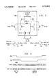
- FIG. 1 is a functional block diagram of a video/graphics processing system embodying the principles of the present invention
- FIG. 2 is a more detailed functional block diagram of the frame buffer of FIG. 1 according to one embodiment of the present invention
- FIG. 3 is a timing diagram illustrating the operation of the circuitry of FIG. 2 during a modify operation
- FIG. 4 is an electrical schematic diagram of the internal write enable signal generation circuitry embodied in the circuitry of FIG. 3;
- FIG. 5 is an electrical schematic diagram of a sense amplifier according to the principles of the present invention.
- FIG. 6 is a timing diagram illustrating the operation of the sense amplifier of FIG. 5 during a modify operation.
- FIG. 1 is a high level functional block diagram of the portion of a processing system 100 controlling the display of graphics and/or video data.
- System 100 includes a central processing unit 101, a system bus 102, a display controller 103, a frame buffer 104, a digital to analog converter (DAC) 105 and a display device 106.
- display controller 103 and frame buffer 104 and DAC 105 are fabricated together on a single integrated circuit chip 107.
- CPU 101 controls the overall operation of system 100, determines the content of graphics data to be displayed on display unit 106 under user commands, and performs various data processing functions.
- CPU 101 may be for example a general purpose microprocessor used in commercial personal computers.
- CPU 101 communicates with the remainder of system 100 via system bus 102, which may be for example a local bus, an ISA bus or a PCI bus.
- DAC 105 receives digital data from controller 103 and outputs in response the analog data required to drive display 106.
- DAC 105 may also include a color palette, YUV to RGB format conversion circuitry, and/or x- and y-zooming circuitry, to name a few options.
- controller 103 is a display controller, such as a VGA controller, which among other things, controls the exchange of graphics and/or video data with frame buffer 103, controls memory refresh, and performs data processing functions such as color expansion.
- a display controller is the "master" for the specific application of display and thus frees up CPU 101 to perform computational tasks.
- the architecture of a display controller optimizes it to perform graphics and video functions in a manner for superior to that of a general purpose microprocessor.
- Controller 103 may also include a color palette, cursor generation hardware, and/or video to graphics conversion circuitry, to name a few options.
- Frame buffer 104 is preferably a dynamic random access memory (DRAM) which includes an array of rows and columns of DRAM cells and associated address and control circuitry such as row and column decoders, read and write buffers, and sense amplifiers. Frame buffer 104 will be discussed in further detail below.
- DRAM dynamic random access memory
- Display 106 may be for example a CRT unit or liquid crystal display, electroluminescent display (ELD), plasma display (PLD), or other type of display device displays images on a display screen as a plurality of pixels. Further, display 106 may be a state-of-the-art device such as a digital micromirror device or a silicon carbide like device which directly accepts digital data. It should also be noted that in alternate embodiments, "display" 106 may be another type of output device such as a laser printer or similar document view/print appliances.
- ELD electroluminescent display
- PLD plasma display
- selected logic operations can be performed on words of data within selected locations within frame buffer 104.
- these principles take advantage of the fact that during AND and OR operations a bit of data in memory being operated on either remains the same or is replaced with the corresponding bit of the modifying data provided by controller 103, depending on the state of the bit of modifying data. This feature is illustrated in Table 1:
- the resulting data remains the same as that already stored in the selected memory cell for the input conditions set forth in the second and forth rows (i.e the modifying data equals a logic 1).
- a read (refresh) of the data within the given cell operation is all that is required to perform the "modification". This can be accomplished with a single RAS/CAS cycle with the write enable signal inactive.
- the resulting data is the same as the modifying data. In this case, all that is required to modify the data in the memory cell is to directly write the modifying data into the memory cell.
- the resulting data remains the same as that already stored in the selected memory cell for the input conditions set forth in the first and third rows (i.e. the modifying data equals a logic 0). Again, all that is required to "modify" the data in the cell is to perform a single RAS/CAS cycle read operation.
- the resulting data is the same as the modifying data and therefore all that is required is for the modifying data to be written directly to the selected memory cell using a conventional single RAS/CAS write cycle.
- the performance of an actual OR operation is not required; data is either refreshed by a read operation or the modifying data is written directly in as a function of the modifying data.
- FIG. 2 is a more detailed functional block diagram of frame buffer 104 according to a preferred embodiment of the present invention.
- Frame buffer 103 includes an array 200 of conventional dynamic random access memory (DRAM) cells arranged in M number of rows and N number of columns. Coupled to array 200 are row decoder circuitry 201, sense amplifiers 202 and column decoder circuitry 203. In the preferred embodiment, N number of sense amplifiers 202, one per each column in array 200, are provided.
- Row decoder circuitry 201 and column decoder circuitry 203 control the access to P-cell storage locations from a selected row of array 200 in a conventional manner in response to row and column addresses latched into address latches 204 by RAS and CAS.
- Frame buffer 104 also includes read/ ⁇ write control circuitry embodying the principles of the present invention.
- Data reads from addressed locations in array 200 are accomplished through read amplifiers 205 and output buffer 206 when the output enable signal is active.
- the write/modify circuitry includes a first data latch 207 which during a conventional write latches data to be written into array 200 and during a modify latches the modifying data.
- Writes and modifications are performed through write buffer 208 which includes P number of conventional write buffers for writing into each accessed P-cell location.
- mode decoder 209 decodes the mode control data latched into a second data latch 210 to determine if an AND or OR operation (and consequently a NOR or NAND operation if complementary modification data is used) is to take place.
- latch 210 receives and holds at least two bits of data which, along with the conventional (external) write enable signal WE, determine if a conventional write or an AND or OR operation has been requested by controller 103.
- frame buffer 104 also includes data pads 211 and associated TTL drivers 212 for receiving data (DQ), addresses, RAS, CAS, WE and OE signals from the controller chip.
- DQ data
- addresses addresses
- RAS address
- CAS address
- WE OE signals
- write buffer 208 writes the modifying data latched into data latch 207 into the addressed memory cell when the modifying data is a logic 0.
- the modifying data is a logic 1
- no write is performed and instead a read takes place (as is known in the art a read operation refreshes the existing data stored in a given accessed memory cell, whatever the state).
- write buffer 208 writes the modifying data latched to data latch 207 into the addressed memory cell when the modifying data is a logic 1; a read occurs when the modifying data is a logic zero.
- the modifying of data is controlled by enabling or disabling write buffer 209.
- FIG. 4 is a logic diagram of preferred circuitry 400 for enabling or disabling write buffer 209 in order to perform the cell data modifications described above.
- this circuitry is located within write buffer 209 along with the write buffers themselves, although in alternate embodiments circuitry 400 may be disposed elsewhere within the chip.
- Circuitry 400 generates an "internal write enable" signal which enables/disables write buffer 208 during data modification operations.
- the internal write enable signal is derived from the conventional write enable signal generated by controller 103 for a conventional write, control signals MODE -- AND and MODE -- OR, and the modifying data.
- circuitry 400 is replicated P number of times such that each of P number of bits accessed in array 200 during a single address cycle can be independently modified. To independently modify P number of bits simultaneously, controller 103 correspondingly generates P number of bits of modifying data which are latched into latch 207.
- Control signals MODE -- AND and MODE -- OR are generated by decoder circuitry 209 from a control word (opcode) latched into data latch 210. Assuming a modification is requested, by controller 103, the external write enable signal is active (i.e. high). When MODE -- AND is high and MODE -- OR is low, an AND operation is selected and the internal write enable signal is active (high) when the modifying data is a logic 0. When bit MODE -- AND is low and bit MODE -- OR is high, an OR operation is selected and the internal write enable signal is active (high) when the modifying data is a logic 1. For a conventional write, MODE -- AND and MODE -- OR are inactive (low) such that the internal write enable signal simply tracks the external write enable signal.
- controller 103 In the case of a NAND operation, the complement of the modifying data is taken and the OR mode is selected. In the case of a NOR operation, the complement of the modifying data is taken and the AND mode is applied. It should be noted that most controllers, such as controller 103, advantageously simultaneously generate complementary data for use in other operations.
- the timing diagram of FIG. 3 illustrates the timing of a given modifying operation.
- the mode select data is latched into data latch 201.
- the falling edge of RAS also latches the row address for the selected location in array 200 into address latch 204.
- the column portion of the address is latched into address latch 204 on the falling edge of the column address strobe (CAS).
- CAS column address strobe
- the modifying data is latched into data latch 207.
- the data within data latch 210 is decoded by mode decoder 209 and presented as MODE -- AND and MODE -- OR to the circuitry shown in FIG. 4, as is the modifying data within data latch 207 and the external write enable signal.
- the modification of the addressed cell or cells proceeds as above.
- FIG. 5 depicts an alternate embodiment of the principles of the present invention.
- this circuit takes advantage of the fact that if the modifying data is a logic 1, then the data in each memory cell stays the same and if the modifying data is a logic 0, the data in each memory cell is always a logic 0.
- this circuit takes advantage of the fact that if the modifying data is a logic 1, the data in each cell will always be logic 1 and if the modifying data is a logic 0, the data in each cell remains the same.
- FIG. 5 a basic latching type sense amplifier 400 is depicted for reference. It should be recognized that the principles of the present invention also apply to many other types of latching sense amplifiers known in the art.
- Two additional transistors 401 and 402 are provided for directly controlling the voltage at nodes 1 and 2 is response to control signals CNTRL1 and CNTRL2 respectively.
- Control signal CNTRL1 is generated from MODE -- AND and the modifying data by inverter 403, NAND gate 404 and inverter 405.
- Control signal CNTRL2 is generated from MODE -- OR and the modifying data by NAND gate 406 and inverter 407.
- all the sense amplifiers 202 would be controlled as shown in FIG. 5 such that an entire row of cells in array 200 would be modified at one time (i.e. each sense amplifier is associated with a pair of controlling transistors 401 and 402, although only one set of control gates 403-407 are required).
- FIG. 6 The timing for logic operations using the embodiment of FIG. 5 are shown in FIG. 6. With the falling edge of RAS, a mode select word is latched into latch 210. At the same time, a bit of modifying data is latched into latch 207. After some circuit delay, the modification, discussed further below, is effected. The modified data may then be read out if desired when CAS goes low (in this case, CAS operates as an enable signal allowing access to the data from the selected columns along the selected row).
- control signal MODE -- AND is set high.
- control signal CNTRL1 goes high and transistor 401 turns on pulling down the true bitline BT. A logic 0 is thereby written into the corresponding memory cell.
- the modifying data is a logic 1
- the data latched into sense amplifier 400 remains the same.
- control signal MODE -- OR is set high.
- control signal CNTRL2 goes high and transistor 402 turns on pulling down the complementary bitline BC (consequently, the true bitline BT is pulled up). A logic 0 is thereby written into the corresponding memory cell.
- the modifying data is a logic 0, the data latched in sense amplifier 400 remains the same. By taking the complement of the modifying data, a NAND operation can similarly be implemented.
- FIG. 1 is a high level functional block diagram of the portion of a processing system 100 controlling the display of graphics and/or video data.
- System 100 includes a central processing unit 101, a system bus 102, a display controller 103, a frame buffer 104, a digital to analog converter (DAC) 105 and a display device 106.
- display controller 103 and frame buffer 104 and DAC 105 are fabricated together on a single integrated circuit chip 107.
- CPU 101 controls the overall operation of system 100, determines the content of graphics data to be displayed on display unit 106 under user commands, and performs various data processing functions.
- CPU 101 may be for example a general purpose microprocessor used in commercial personal computers.
- CPU 101 communicates with the remainder of system 100 via system bus 102, which may be for example a local bus, an ISA bus or a PCI bus.
- DAC 105 receives digital data from controller 103 and outputs in response the analog data required to drive display 106.
- DAC 105 may also include a color palette, YUV to RGB format conversion circuitry, and/or x- and y-zooming circuitry, to name a few options.
- controller 103 is a display controller, such as a VGA controller, which among other things, controls the exchange of graphics and/or video data with frame buffer 103, controls memory refresh, and performs data processing functions such as color expansion.
- a display controller is the "master" for the specific application of display and thus frees up CPU 101 to perform computational tasks.
- the architecture of a display controller optimizes it to perform graphics and video functions in a manner for superior to that of a general purpose microprocessor.
- Controller 103 may also include a color palette, cursor generation hardware, and/or video to graphics conversion circuitry, to name a few options.
- Frame buffer 104 is preferably a dynamic random access memory (DRAM) which includes an array of rows and columns of DRAM cells and associated address and control circuitry such as row and column decoders, read and write buffers, and sense amplifiers. Frame buffer 104 will be discussed in further detail below.
- DRAM dynamic random access memory
- Display 106 may be for example a CRT unit or liquid crystal display, electroluminescent display (ELD), plasma display (PLD), or other type of display device displays images on a display screen as a plurality of pixels. Further, display 106 may be a state-of-the-art device such as a digital micromirror device or a silicon carbide like device which directly accepts digital data. It should also be noted that in alternate embodiments, "display" 106 may be another type of output device such as a laser printer or similar document view/print appliances.
- ELD electroluminescent display
- PLD plasma display
- selected logic operations can be performed on words of data within selected locations within frame buffer 104.
- these principles take advantage of the fact that during AND and OR operations a bit of data in memory being operated on either remains the same or is replaced with the corresponding bit of the modifying data provided by controller 103, depending on the state of the bit of modifying data. This feature is illustrated in Table 1:
- the resulting data remains the same as that already stored in the selected memory cell for the input conditions set forth in the second and forth rows (i.e the modifying data equals a logic 1).
- a read (refresh) of the data within the given cell operation is all that is required to perform the "modification". This can be accomplished with a single RAS/CAS cycle with the write enable signal inactive.
- the resulting data is the same as the modifying data. In this case, all that is required to modify the data in the memory cell is to directly write the modifying data into the memory cell.
- the resulting data remains the same as that already stored in the selected memory cell for the input conditions set forth in the first and third rows (i.e. the modifying data equals a logic 0). Again, all that is required to "modify" the data in the cell is to perform a single RAS/CAS cycle read operation.
- the resulting data is the same as the modifying data and therefore all that is required is for the modifying data to be written directly to the selected memory cell using a conventional single RAS/CAS write cycle.
- the performance of an actual OR operation is not required; data is either refreshed by a read operation or the modifying data is written directly in as a function of the modifying data.
- FIG. 2 is a more detailed functional block diagram of frame buffer 104 according to a preferred embodiment of the present invention.
- Frame buffer 103 includes an array 200 of conventional dynamic random access memory (DRAM) cells arranged in M number of rows and N number of columns. Coupled to array 200 are row decoder circuitry 201, sense amplifiers 202 and column decoder circuitry 203. In the preferred embodiment, N number of sense amplifiers 202, one per each column in array 200, are provided.
- Row decoder circuitry 201 and column decoder circuitry 203 control the access to P-cell storage locations from a selected row of array 200 in a conventional manner in response to row and column addresses latched into address latches 204 by RAS and CAS.
- Frame buffer 104 also includes read/ ⁇ write control circuitry embodying the principles of the present invention.
- Data reads from addressed locations in array 200 are accomplished through read amplifiers 205 and output buffer 206 when the output enable signal is active.
- the write/modify circuitry includes a first data latch 207 which during a conventional write latches data to be written into array 200 and during a modify latches the modifying data.
- Writes and modifications are performed through write buffer 208 which includes P number of conventional write buffers for writing into each accessed P-cell location.
- mode decoder 209 decodes the mode control data latched into a second data latch 210 to determine if an AND or OR operation (and consequently a NOR or NAND operation if complementary modification data is used) is to take place.
- latch 210 receives and holds at least two bits of data which, along with the conventional (external) write enable signal WE, determine if a conventional write or an AND or OR operation has been requested by controller 103.
- frame buffer 104 also includes data pads 211 and associated TTL drivers 212 for receiving data (DQ), addresses, RAS, CAS, WE and OE signals from the controller chip.
- DQ data
- addresses addresses
- RAS address
- CAS address
- WE OE signals
- write buffer 208 writes the modifying data latched into data latch 207 into the addressed memory cell when the modifying data is a logic 0.
- the modifying data is a logic 1
- no write is performed and instead a read takes place (as is known in the art a read operation refreshes the existing data stored in a given accessed memory cell, whatever the state).
- write buffer 208 writes the modifying data latched to data latch 207 into the addressed memory cell when the modifying data is a logic 1; a read occurs when the modifying data is a logic zero.
- the modifying of data is controlled by enabling or disabling write buffer 209.
- FIG. 4 is a logic diagram of preferred circuitry 400 for enabling or disabling write buffer 209 in order to perform the cell data modifications described above.
- this circuitry is located within write buffer 209 along with the write buffers themselves, although in alternate embodiments circuitry 400 may be disposed elsewhere within the chip.
- Circuitry 400 generates an "internal write enable" signal which enables/disables write buffer 208 during data modification operations.
- the internal write enable signal is derived from the conventional write enable signal generated by controller 103 for a conventional write, control signals MODE -- AND and MODE -- OR, and the modifying data.
- circuitry 400 is replicated P number of times such that each of P number of bits accessed in array 200 during a single address cycle can be independently modified. To independently modify P number of bits simultaneously, controller 103 correspondingly generates P number of bits of modifying data which are latched into latch 207.
- Control signals MODE -- AND and MODE -- OR are generated by decoder circuitry 209 from a control word (opcode) latched into data latch 210. Assuming a modification is requested, by controller 103, the external write enable signal is active (i.e. high). When MODE -- AND is high and MODE -- OR is low, an AND operation is selected and the internal write enable signal is active (high) when the modifying data is a logic 0. When bit MODE -- AND is low and bit MODE -- OR is high, an OR operation is selected and the internal write enable signal is active (high) when the modifying data is a logic 1. For a conventional write, MODE -- AND and MODE -- OR are inactive (low) such that the internal write enable signal simply tracks the external write enable signal.
- controller 103 In the case of a NAND operation, the complement of the modifying data is taken and the OR mode is selected. In the case of a NOR operation, the complement of the modifying data is taken and the AND mode is applied. It should be noted that most controllers, such as controller 103, advantageously simultaneously generate complementary data for use in other operations.
- the timing diagram of FIG. 3 illustrates the timing of a given modifying operation.
- the mode select data is latched into data latch 201.
- the falling edge of RAS also latches the row address for the selected location in array 200 into address latch 204.
- the column portion of the address is latched into address latch 204 on the falling edge of the column address strobe (CAS).
- CAS column address strobe
- the modifying data is latched into data latch 207.
- the data within data latch 210 is decoded by mode decoder 209 and presented as MODE -- AND and MODE -- OR to the circuitry shown in FIG. 4, as is the modifying data within data latch 207 and the external write enable signal.
- the modification of the addressed cell or cells proceeds as above.
- FIG. 5 depicts an alternate embodiment of the principles of the present invention.
- this circuit takes advantage of the fact that if the modifying data is a logic 1, then the data in each memory cell stays the same and if the modifying data is a logic 0, the data in each memory cell is always a logic 0.
- this circuit takes advantage of the fact that if the modifying data is a logic 1, the data in each cell will always be logic 1 and if the modifying data is a logic 0, the data in each cell remains the same.
- FIG. 5 a basic latching type sense amplifier 400 is depicted for reference. It should be recognized that the principles of the present invention also apply to many other types of latching sense amplifiers known in the art.
- Two additional transistors 401 and 402 are provided for directly controlling the voltage at nodes 1 and 2 is response to control signals CNTRL1 and CNTRL2 respectively.
- Control signal CNTRL1 is generated from MODE -- AND and the modifying data by inverter 403, NAND gate 404 and inverter 405.
- Control signal CNTRL2 is generated from MODE -- OR and the modifying data by NAND gate 406 and inverter 407.
- all the sense amplifiers 202 would be controlled as shown in FIG. 5 such that an entire row of cells in array 200 would be modified at one time (i.e. each sense amplifier is associated with pair of controlling transistors 401 and 402, although only one set of control gates 403-407 are required).
- FIG. 6 The timing for logic operations using the embodiment of FIG. 5 are shown in FIG. 6. With the falling edge of RAS, a mode select word is latched into latch 210. At the same time, a bit of modifying data is latched into latch 207. After some circuit delay, the modification, discussed further below, is effected. The modified data may then be read out if desired when CAS goes low (in this case, CAS operates as an enable signal allowing access to the data from the selected columns along the selected row).
- control signal MODE -- AND is set high.
- control signal CNTRL1 goes high and transistor 401 turns on pulling down the true bitline BT. A logic 0 is thereby written into the corresponding memory cell.
- the modifying data is a logic 1
- the data latched into sense amplifier 400 remains the same.
- control signal MODE -- OR is set high.
- control signal CNTRL2 goes high and transistor 402 turns on pulling down the complementary bitline BC (consequently, the true bitline BT is pulled up). A logic 0 is thereby written into the corresponding memory cell.
- the modifying data is a logic 0, the data latched in sense amplifier 400 remains the same. By taking the complement of the modifying data, a NAND operation can similarly be implemented.
Abstract
Description
______________________________________
OPERANDS                    RESULTS
CELL DATA  MODIFYING DATA   AND    OR
______________________________________
0          0                0      0
0          1                0      1
1          0                0      1
1          1                1      1
______________________________________
______________________________________
OPERANDS                    RESULTS
CELL DATA  MODIFYING DATA   AND    OR
______________________________________
0          0                0      0
0          1                0      1
1          0                0      1
1          1                1      1
______________________________________
Claims (14)
Priority Applications (10)
| Application Number | Priority Date | Filing Date | Title |
|---|---|---|---|
| US08/424,653 US5732024A (en) | 1995-04-19 | 1995-04-19 | Circuits, systems and methods for modifying data stored in a memory using logic operations |
| JP8531977A JPH11504148A (en) | 1995-04-19 | 1996-04-19 | Circuit, system, and method for changing data stored in memory using logical operation |
| KR1019970707383A KR19990007860A (en) | 1995-04-19 | 1996-04-19 | Circuit, system and method for modifying data stored in memory using logical operations |
| PCT/US1996/005523 WO1996033498A1 (en) | 1995-04-19 | 1996-04-19 | Circuits, systems and methods for modifying data stored in a memory using logic operations |
| EP96912973A EP0823116B1 (en) | 1995-04-19 | 1996-04-19 | Circuits, systems and methods for modifying data stored in a memory using logic operations |
| DE69602742T DE69602742T2 (en) | 1995-04-19 | 1996-04-19 | CIRCUITS, SYSTEMS AND METHODS FOR CHANGING STORAGE DATA USING LOGICAL FUNCTIONS |
| US08/902,674 US5914900A (en) | 1995-04-19 | 1997-07-30 | Circuits, systems and methods for modifying data stored in a memory using logic operations |
| US08/903,390 US5910919A (en) | 1995-04-19 | 1997-07-30 | Circuits, systems and methods for modifying data stored in a memory using logic operations |
| US08/903,317 US5909401A (en) | 1995-04-19 | 1997-07-30 | Sensing circuitry with boolean logic |
| HK98108912A HK1007912A1 (en) | 1995-04-19 | 1998-07-07 | Circuits systems and methods for modifying data stored in a memory using logic operations |
Applications Claiming Priority (1)
| Application Number | Priority Date | Filing Date | Title |
|---|---|---|---|
| US08/424,653 US5732024A (en) | 1995-04-19 | 1995-04-19 | Circuits, systems and methods for modifying data stored in a memory using logic operations |
Related Child Applications (3)
| Application Number | Title | Priority Date | Filing Date |
|---|---|---|---|
| US08/902,674 Division US5914900A (en) | 1995-04-19 | 1997-07-30 | Circuits, systems and methods for modifying data stored in a memory using logic operations |
| US08/903,317 Division US5909401A (en) | 1995-04-19 | 1997-07-30 | Sensing circuitry with boolean logic |
| US08/903,390 Division US5910919A (en) | 1995-04-19 | 1997-07-30 | Circuits, systems and methods for modifying data stored in a memory using logic operations |
Publications (1)
| Publication Number | Publication Date |
|---|---|
| US5732024A true US5732024A (en) | 1998-03-24 |
Family
ID=23683379
Family Applications (4)
| Application Number | Title | Priority Date | Filing Date |
|---|---|---|---|
| US08/424,653 Expired - Lifetime US5732024A (en) | 1995-04-19 | 1995-04-19 | Circuits, systems and methods for modifying data stored in a memory using logic operations |
| US08/903,390 Expired - Lifetime US5910919A (en) | 1995-04-19 | 1997-07-30 | Circuits, systems and methods for modifying data stored in a memory using logic operations |
| US08/903,317 Expired - Lifetime US5909401A (en) | 1995-04-19 | 1997-07-30 | Sensing circuitry with boolean logic |
| US08/902,674 Expired - Lifetime US5914900A (en) | 1995-04-19 | 1997-07-30 | Circuits, systems and methods for modifying data stored in a memory using logic operations |
Family Applications After (3)
| Application Number | Title | Priority Date | Filing Date |
|---|---|---|---|
| US08/903,390 Expired - Lifetime US5910919A (en) | 1995-04-19 | 1997-07-30 | Circuits, systems and methods for modifying data stored in a memory using logic operations |
| US08/903,317 Expired - Lifetime US5909401A (en) | 1995-04-19 | 1997-07-30 | Sensing circuitry with boolean logic |
| US08/902,674 Expired - Lifetime US5914900A (en) | 1995-04-19 | 1997-07-30 | Circuits, systems and methods for modifying data stored in a memory using logic operations |
Country Status (7)
| Country | Link |
|---|---|
| US (4) | US5732024A (en) |
| EP (1) | EP0823116B1 (en) |
| JP (1) | JPH11504148A (en) |
| KR (1) | KR19990007860A (en) |
| DE (1) | DE69602742T2 (en) |
| HK (1) | HK1007912A1 (en) |
| WO (1) | WO1996033498A1 (en) |
Cited By (3)
| Publication number | Priority date | Publication date | Assignee | Title |
|---|---|---|---|---|
| EP1041570A1 (en) * | 1999-03-30 | 2000-10-04 | NEC Corporation | Semiconductor memory |
| US6301189B1 (en) | 1999-06-28 | 2001-10-09 | Hyundai Electronics Industries Co., Ltd. | Apparatus for generating write control signals applicable to double data rate SDRAM |
| US20040268207A1 (en) * | 2003-05-21 | 2004-12-30 | Engim, Inc. | Systems and methods for implementing a rate converting, low-latency, low-power block interleaver |
Families Citing this family (2)
| Publication number | Priority date | Publication date | Assignee | Title |
|---|---|---|---|---|
| FR2812963B1 (en) * | 2000-08-11 | 2003-07-25 | St Microelectronics Sa | METHOD AND CIRCUIT FOR CONTROLLING CELLS OF A PLASMA SCREEN |
| US6549470B2 (en) * | 2000-08-31 | 2003-04-15 | United Memories, Inc. | Small signal, low power read data bus driver for integrated circuit devices incorporating memory arrays |
Citations (7)
| Publication number | Priority date | Publication date | Assignee | Title |
|---|---|---|---|---|
| JPS5682928A (en) * | 1979-12-07 | 1981-07-07 | Nec Corp | Data processor |
| EP0209050A2 (en) * | 1985-07-08 | 1987-01-21 | Nec Corporation | Semiconductor memory capable of executing logical operation |
| GB2225657A (en) * | 1988-12-02 | 1990-06-06 | Ncr Co | Random access memory/logic system |
| US5195056A (en) * | 1987-05-21 | 1993-03-16 | Texas Instruments, Incorporated | Read/write memory having an on-chip input data register, having pointer circuits between a serial data register and input/output buffer circuits |
| JPH05298178A (en) * | 1992-04-13 | 1993-11-12 | Nec Corp | Semiconductor integrated circuit |
| US5432743A (en) * | 1992-06-30 | 1995-07-11 | Nec Corporation | Semiconductor dynamic RAM for image processing |
| US5544115A (en) * | 1992-01-24 | 1996-08-06 | Mitsubishi Denki Kabushiki Kaisha | Semiconductor memory device allowing selection of the number of sense amplifiers to be activated simultaneously |
Family Cites Families (4)
| Publication number | Priority date | Publication date | Assignee | Title |
|---|---|---|---|---|
| GB222567A (en) * | 1923-07-03 | 1924-10-03 | Maria Scholz | Process for dyeing textile fabric, paper and like materials |
| ES2022698B3 (en) * | 1988-02-26 | 1991-12-01 | Ibm | DOUBLE PHASE DIRECTION AMPLIFIER FOR RANDOM ACCESS MEMORIES. |
| JPH0636555A (en) * | 1992-05-20 | 1994-02-10 | Nec Corp | Dynamic semiconductor memory and device for generating image data |
| JPH0676565A (en) * | 1992-06-30 | 1994-03-18 | Nec Corp | Semiconductor memory device |
-
1995
- 1995-04-19 US US08/424,653 patent/US5732024A/en not_active Expired - Lifetime
-
1996
- 1996-04-19 DE DE69602742T patent/DE69602742T2/en not_active Expired - Fee Related
- 1996-04-19 KR KR1019970707383A patent/KR19990007860A/en not_active Application Discontinuation
- 1996-04-19 EP EP96912973A patent/EP0823116B1/en not_active Expired - Lifetime
- 1996-04-19 WO PCT/US1996/005523 patent/WO1996033498A1/en not_active Application Discontinuation
- 1996-04-19 JP JP8531977A patent/JPH11504148A/en active Pending
-
1997
- 1997-07-30 US US08/903,390 patent/US5910919A/en not_active Expired - Lifetime
- 1997-07-30 US US08/903,317 patent/US5909401A/en not_active Expired - Lifetime
- 1997-07-30 US US08/902,674 patent/US5914900A/en not_active Expired - Lifetime
-
1998
- 1998-07-07 HK HK98108912A patent/HK1007912A1/en not_active IP Right Cessation
Patent Citations (7)
| Publication number | Priority date | Publication date | Assignee | Title |
|---|---|---|---|---|
| JPS5682928A (en) * | 1979-12-07 | 1981-07-07 | Nec Corp | Data processor |
| EP0209050A2 (en) * | 1985-07-08 | 1987-01-21 | Nec Corporation | Semiconductor memory capable of executing logical operation |
| US5195056A (en) * | 1987-05-21 | 1993-03-16 | Texas Instruments, Incorporated | Read/write memory having an on-chip input data register, having pointer circuits between a serial data register and input/output buffer circuits |
| GB2225657A (en) * | 1988-12-02 | 1990-06-06 | Ncr Co | Random access memory/logic system |
| US5544115A (en) * | 1992-01-24 | 1996-08-06 | Mitsubishi Denki Kabushiki Kaisha | Semiconductor memory device allowing selection of the number of sense amplifiers to be activated simultaneously |
| JPH05298178A (en) * | 1992-04-13 | 1993-11-12 | Nec Corp | Semiconductor integrated circuit |
| US5432743A (en) * | 1992-06-30 | 1995-07-11 | Nec Corporation | Semiconductor dynamic RAM for image processing |
Non-Patent Citations (2)
| Title |
|---|
| Patent Abstracts of Japan vol. 18, No. 264, p. 174 on May 19, 1994 Abstract JPA06036555. * |
| Patent Abstracts of Japan vol. 18, No. 333, p. 1759 on Jun. 23, 1994 Abstract No. JPA06076565. * |
Cited By (4)
| Publication number | Priority date | Publication date | Assignee | Title |
|---|---|---|---|---|
| EP1041570A1 (en) * | 1999-03-30 | 2000-10-04 | NEC Corporation | Semiconductor memory |
| US6292404B1 (en) | 1999-03-30 | 2001-09-18 | Nec Corporation | Semiconductor memory |
| US6301189B1 (en) | 1999-06-28 | 2001-10-09 | Hyundai Electronics Industries Co., Ltd. | Apparatus for generating write control signals applicable to double data rate SDRAM |
| US20040268207A1 (en) * | 2003-05-21 | 2004-12-30 | Engim, Inc. | Systems and methods for implementing a rate converting, low-latency, low-power block interleaver |
Also Published As
| Publication number | Publication date |
|---|---|
| DE69602742T2 (en) | 2000-01-13 |
| US5910919A (en) | 1999-06-08 |
| WO1996033498A1 (en) | 1996-10-24 |
| KR19990007860A (en) | 1999-01-25 |
| US5909401A (en) | 1999-06-01 |
| HK1007912A1 (en) | 1999-04-30 |
| EP0823116A1 (en) | 1998-02-11 |
| EP0823116B1 (en) | 1999-06-02 |
| DE69602742D1 (en) | 1999-07-08 |
| JPH11504148A (en) | 1999-04-06 |
| US5914900A (en) | 1999-06-22 |
Similar Documents
| Publication | Publication Date | Title |
|---|---|---|
| US5920885A (en) | Dynamic random access memory with a normal precharge mode and a priority precharge mode | |
| US5506810A (en) | Dual bank memory and systems using the same | |
| US6041389A (en) | Memory architecture using content addressable memory, and systems and methods using the same | |
| JP4128234B2 (en) | Memory device, processing system, method for controlling memory device and method for operating dynamic random access memory | |
| US5473566A (en) | Memory architecture and devices, systems and methods utilizing the same | |
| US5442588A (en) | Circuits and methods for refreshing a dual bank memory | |
| US5945974A (en) | Display controller with integrated half frame buffer and systems and methods using the same | |
| US5654932A (en) | Memory devices with selectable access type and methods using the same | |
| JPH05274862A (en) | Semiconductor memory device | |
| JP3105884B2 (en) | Display controller for memory display device | |
| US5732024A (en) | Circuits, systems and methods for modifying data stored in a memory using logic operations | |
| KR100490703B1 (en) | How to configure single-chip frame buffers, frame buffers, display subsystems, and frame buffers | |
| US5906003A (en) | Memory device with an externally selectable-width I/O port and systems and methods using the same | |
| KR100472478B1 (en) | Method and apparatus for controlling memory access | |
| KR950009076B1 (en) | Dual port memory and control method | |
| JPH0430119B2 (en) | ||
| KR20060076871A (en) | Apparatus and method for controlling graphic ram of display driver ic | |
| JPH05258557A (en) | Semiconductor memory device | |
| JPH04344385A (en) | Semiconductor storage device |
Legal Events
| Date | Code | Title | Description |
|---|---|---|---|
| AS | Assignment |
Owner name: CIRRUS LOGIC, INC., CALIFORNIA Free format text: ASSIGNMENT OF ASSIGNORS INTEREST;ASSIGNORS:SHARMA, SUDHIR;RUNAS, MICHAEL E.;NALLY, ROBERT M.;REEL/FRAME:007477/0308;SIGNING DATES FROM 19950414 TO 19950417 |
|
| AS | Assignment |
Owner name: BANK OF AMERICA NATIONAL TRUST & SAVINGS ASSOCIATI Free format text: SECURITY AGREEMENT;ASSIGNOR:CIRRUS LOGIC, INC.;REEL/FRAME:008113/0001 Effective date: 19960430 |
|
| FEPP | Fee payment procedure |
Free format text: PAYOR NUMBER ASSIGNED (ORIGINAL EVENT CODE: ASPN); ENTITY STATUS OF PATENT OWNER: LARGE ENTITY |
|
| STCF | Information on status: patent grant |
Free format text: PATENTED CASE |
|
| FEPP | Fee payment procedure |
Free format text: PAYER NUMBER DE-ASSIGNED (ORIGINAL EVENT CODE: RMPN); ENTITY STATUS OF PATENT OWNER: LARGE ENTITY Free format text: PAYOR NUMBER ASSIGNED (ORIGINAL EVENT CODE: ASPN); ENTITY STATUS OF PATENT OWNER: LARGE ENTITY |
|
| FPAY | Fee payment |
Year of fee payment: 4 |
|
| FPAY | Fee payment |
Year of fee payment: 8 |
|
| FPAY | Fee payment |
Year of fee payment: 12 |
|
| FEPP | Fee payment procedure |
Free format text: PAYER NUMBER DE-ASSIGNED (ORIGINAL EVENT CODE: RMPN); ENTITY STATUS OF PATENT OWNER: LARGE ENTITY Free format text: PAYOR NUMBER ASSIGNED (ORIGINAL EVENT CODE: ASPN); ENTITY STATUS OF PATENT OWNER: LARGE ENTITY |
|
| AS | Assignment |
Owner name: CIRRUS LOGIC, INC., TEXAS Free format text: RELEASE BY SECURED PARTY;ASSIGNOR:BANK OF AMERIC NATIONAL TRUST & SAVINGS ASSOCIATION;REEL/FRAME:024864/0562 Effective date: 20100820 |
|
| AS | Assignment |
Owner name: CIRRUS LOGIC, INC., TEXAS Free format text: CORRECTIVE ASSIGNMENT TO CORRECT THE ASSIGNOR'S NAME PREVIOUSLY RECORDED ON REEL 024864 FRAME 0562. ASSIGNOR(S) HEREBY CONFIRMS THE RELEASE OF SECURITY AGREEMENT;ASSIGNOR:BANK OF AMERICA NATIONAL TRUST & SAVINGS ASSOCIATION;REEL/FRAME:024864/0797 Effective date: 20100820 |
|
| AS | Assignment |
Owner name: HUAI TECHNOLOGIES, LLC, DELAWARE Free format text: ASSIGNMENT OF ASSIGNORS INTEREST;ASSIGNOR:CIRRUS LOGIC, INC.;REEL/FRAME:025039/0292 Effective date: 20100824 |
|
| AS | Assignment |
Owner name: INTELLECTUAL VENTURES II LLC, DELAWARE Free format text: MERGER;ASSIGNOR:HUAI TECHNOLOGIES, LLC;REEL/FRAME:025446/0029 Effective date: 20101207 |