US5694031A - Voltage regulator with differential current steering stage - Google Patents
Voltage regulator with differential current steering stage Download PDFInfo
- Publication number
- US5694031A US5694031A US08/632,977 US63297796A US5694031A US 5694031 A US5694031 A US 5694031A US 63297796 A US63297796 A US 63297796A US 5694031 A US5694031 A US 5694031A
- Authority
- US
- United States
- Prior art keywords
- stage
- voltage
- output
- coupled
- differential current
- Prior art date
- Legal status (The legal status is an assumption and is not a legal conclusion. Google has not performed a legal analysis and makes no representation as to the accuracy of the status listed.)
- Expired - Lifetime
Links
Images

Classifications
-
- G—PHYSICS
- G05—CONTROLLING; REGULATING
- G05F—SYSTEMS FOR REGULATING ELECTRIC OR MAGNETIC VARIABLES
- G05F3/00—Non-retroactive systems for regulating electric variables by using an uncontrolled element, or an uncontrolled combination of elements, such element or such combination having self-regulating properties
- G05F3/02—Regulating voltage or current
- G05F3/08—Regulating voltage or current wherein the variable is DC
- G05F3/10—Regulating voltage or current wherein the variable is DC using uncontrolled devices with non-linear characteristics
- G05F3/16—Regulating voltage or current wherein the variable is DC using uncontrolled devices with non-linear characteristics being semiconductor devices
- G05F3/20—Regulating voltage or current wherein the variable is DC using uncontrolled devices with non-linear characteristics being semiconductor devices using diode- transistor combinations
- G05F3/22—Regulating voltage or current wherein the variable is DC using uncontrolled devices with non-linear characteristics being semiconductor devices using diode- transistor combinations wherein the transistors are of the bipolar type only
- G05F3/222—Regulating voltage or current wherein the variable is DC using uncontrolled devices with non-linear characteristics being semiconductor devices using diode- transistor combinations wherein the transistors are of the bipolar type only with compensation for device parameters, e.g. Early effect, gain, manufacturing process, or external variations, e.g. temperature, loading, supply voltage
- G05F3/227—Regulating voltage or current wherein the variable is DC using uncontrolled devices with non-linear characteristics being semiconductor devices using diode- transistor combinations wherein the transistors are of the bipolar type only with compensation for device parameters, e.g. Early effect, gain, manufacturing process, or external variations, e.g. temperature, loading, supply voltage producing a current or voltage as a predetermined function of the supply voltage
Definitions
- the present invention relates to voltage regulator circuits, and in particular to voltage regulators for use in a two-lead switch environment.
- Voltage regulator circuits are well known for providing a precise voltage reference output. In most environments, the voltage regulator operates off a supply voltage which can vary, and it is the job of the voltage regulator to provide a precise voltage reference output independent of fluctuations in the supply voltage.
- a voltage regulator may be required where the supply voltage can vary greatly.
- a switch such as a proximity switch
- the voltage can vary significantly depending upon whether the switch is open or closed. In the open switch configuration, some small trickle current must be made available to power circuitry.
- a typical voltage regulator will reference its control circuitry to the supply voltage itself, thus making it susceptible to errors due to wide variations in the supply voltage. Error correction circuitry is also typically connected to the supply voltage, and thus the amount of error correction possible is limited for wide variations in the supply voltage.
- PSRR power supply rejection ratio
- the present invention provides an improved voltage regulator which can operate in a two-lead environment with a widely varying power supply.
- the voltage regulator of the invention has an output circuit stage connected between a supply voltage and a reference voltage.
- a pass transistor as one leg of a differential current steering stage, provides drive current to the output stage.
- a bandgap error amplifier is coupled between the reference voltage output and the pass transistor to shunt current from the pass transistor when the reference voltage varies from the desired voltage value.
- the bandgap error amplifier is coupled between the reference voltage output and a bandgap reference voltage output.
- a transistor in the bandgap error amplifier couples the reference voltage output to the differential current steering stage.
- the differential current steering stage has one input driven by the bandgap error amplifier, and the other input is a reference voltage provided by a voltage clamp.
- the differential current steering stage regulates the current to the output stage.
- the bandgap error amplifier By connecting the bandgap error amplifier to the reference voltage output, rather than the supply voltage, it is insulated from wide variations in the supply voltage. Similarly, using a transistor in the bandgap regulator which is also connected to the voltage reference output, to drive the error amplifier, isolates the error amplifier from the voltage supply fluctuations. Such a circuit as the present invention thus requires a start-up circuit to provide current to the output stage from the voltage supply until the voltage reference output comes up to a sufficient voltage to power the bandgap regulator.
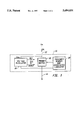
- FIG. 1 is a block diagram of a proximity switch circuit into which the present invention could be incorporated.
- FIG. 2 is a circuit diagram of a voltage regulator according to one embodiment of the present invention.
- FIG. 1 is a block diagram of one embodiment of a switching circuit into which the present invention could be incorporated.
- a switching circuit card 10 is connected between two leads 12 and 14.
- Lead 12 is connected to the load, R L , and through the load to a voltage supply, V S .
- Lead 14 is connected to ground.
- a proximity switch 16 connects the load to ground, to close the circuit when enabled by a proximity sensor and associated circuitry 18. Both of these circuits need a reference voltage to operate on, typically a voltage reference, REF, and a bandgap voltage reference, BGREF. These are provided by a voltage regulator circuit 20. Voltage regulator 20 receives its power, V cc , from the first lead 12, and has its ground connected to the second lead 14. As can be seen, the voltage on lead 12 can vary widely depending upon whether proximity switch 16 is open or closed.
- circuit 10 operates where the supply voltage can vary from 10 volts to 55 volts for the supply voltage. Between the on state and off state of the switch, V CC can vary from 2.5 volts to 55 volts. As can be seen, voltage regulator 20 must thus have a high power supply rejection ratio (PSRR) to operate in such an environment.
- PSRR power supply rejection ratio
- FIG. 2 is a circuit diagram of one embodiment of a voltage regulator 20 according to the present invention.
- the regulator includes an output stage 22 which provides the output voltage, REF, on line 24.
- the output stage is driven by one leg of a differential current steering stage 26, which is stabilized at the appropriate voltage reference output level by a bandgap error amplifier 30.
- bias circuit 28 is referenced to the voltage reference output, 24, and not the supply voltage, V CC , on line 12.
- a bandgap error amplifier 30 provides a bandgap voltage output (BGREF) on a line 32. This voltage is provided at a fixed value by the bandgap error amplifier, and the reference voltage on line 24 is referenced to this voltage by virtue of a resistor divider consisting of resistors RB12 and RB7. Note, again, that bandgap error amplifier 30 is referenced to the voltage reference output line 24, and not to the supply voltage 12.
- BGREF bandgap voltage output
- a start-up circuit 34 is used to provide enough current to the base of transistor Q11 in differential current steering stage 26 to provide the initial power to bring up the voltage on voltage reference line 24.
- the voltage provided by this current is limited by a voltage clamp circuit 36.
- Regulator 20 includes the differential current steering stage 26, consisting of transistors Q11 and Q12. Again, transistor Q12 has its collector connected to the voltage reference output line 24, not to the supply voltage 12. Shunt current is provided through transistor Q12 to resistor RB8 in the differential current steering stage 26. This essentially shunts, or steals current from the emitter of Q11 to provide feedback to keep the output stage driving the voltage reference at the appropriate voltage.
- the differential current steering stage of Q11 and Q12 is in a common-emitter configuration, with Q12 connected to an input of this stage, and Q11 connected to a reference voltage from voltage clamp 36. This stage converts the voltage at Q12 into a current to drive BGREF, which feeds back through bandgap error amplifier 30.
- transistors Q23 and JEF1 provide base drive to transistor Q11.
- Additional base drive in the form of positive feedback, appears through bias circuit 28 consisting of resistor RI36 and transistor Q28, configured as a diode. This feedback appears as soon as the reference voltage on line 24 exceeds two VBEs. When this reference voltage reaches 3VBEs, positive feedback gain reduces to a very low value preventing instability due to positive feedback.
- This positive feedback loop drives the Q11 transistor with its peak output current, with the Q11 transistor in turn driving the output stage 22.
- Output stage 22 consists of a PNP Darlington pair of transistors Q15 and Q13.
- the output transistor Q13 charges a compensation capacitor connected to line 24, shown as capacitor C in FIG. 1. This capacitor is charged to the regulated output voltage level.
- a resistive divider circuit consisting of resistors RB12 and RB7 is connected between the reference voltage line 24 and ground, providing feedback to the bandgap reference line 32.
- a transistor Q1 has a collector output which remains off for BGREF voltages below the bandgap voltage value. When the bandgap voltage BGREF reaches its equilibrium value, transistor Q1 turns on, activating the current steering stage.
- the input voltage to the current steering stage is generated by the diode-connected transistor Q31 and resistor RB14.
- the base voltage of Q12 increases, forcing Q12 to conduct, which steals or shunts the base drive from the output stage.
- the current through Q12 will increase until an equilibrium is reached.
- the bandgap reference maintains its design value. In the embodiment shown, the design value is 1.25 volts.
- the reference voltage remains in regulation at a level defined by the resistor divider gain multiplied by the bandgap reference voltage.
- the differential current steering stage input presents the bandgap error amplifier output with a near constant impedance load. Hence the bandgap AC characteristics remain near constant over the entire reference current load range.
- the output stage requires an external capacitor with a minimum value of 1 uF to establish a dominant pole in the closed loop.
- the transistor Q11 is configured in the common base configuration which gives it high output impedance and its BVCER breakdown voltage approaches its collector base breakdown, lending it to 60V operation without going into collector-emitter breakdown, which normally occurs at 40V.
- the emitter area of the Q19 and Q20 diodes is increased to 10 times that of the Q11 transistor.
- the Q11 emitter drops by approximately 100 mV, at -20° C., below the level that it would reside at if there was no difference in the emitter area.
- the regulator can provide very high power supply rejection.
- a circuit constructed as set forth in FIG. 2 has been measured to provide a PSRR in excess of 80 dB.
Landscapes
- Engineering & Computer Science (AREA)
- Microelectronics & Electronic Packaging (AREA)
- Physics & Mathematics (AREA)
- Nonlinear Science (AREA)
- Electromagnetism (AREA)
- General Physics & Mathematics (AREA)
- Radar, Positioning & Navigation (AREA)
- Automation & Control Theory (AREA)
- Continuous-Control Power Sources That Use Transistors (AREA)
Abstract
Description
Claims (13)
Priority Applications (1)
| Application Number | Priority Date | Filing Date | Title |
|---|---|---|---|
| US08/632,977 US5694031A (en) | 1996-04-16 | 1996-04-16 | Voltage regulator with differential current steering stage |
Applications Claiming Priority (1)
| Application Number | Priority Date | Filing Date | Title |
|---|---|---|---|
| US08/632,977 US5694031A (en) | 1996-04-16 | 1996-04-16 | Voltage regulator with differential current steering stage |
Publications (1)
| Publication Number | Publication Date |
|---|---|
| US5694031A true US5694031A (en) | 1997-12-02 |
Family
ID=24537783
Family Applications (1)
| Application Number | Title | Priority Date | Filing Date |
|---|---|---|---|
| US08/632,977 Expired - Lifetime US5694031A (en) | 1996-04-16 | 1996-04-16 | Voltage regulator with differential current steering stage |
Country Status (1)
| Country | Link |
|---|---|
| US (1) | US5694031A (en) |
Cited By (9)
| Publication number | Priority date | Publication date | Assignee | Title |
|---|---|---|---|---|
| US5920183A (en) * | 1997-10-24 | 1999-07-06 | Stmicroelectronics, Inc. | Voltage regulator for regulating its output voltage selectively with respect to more than one voltage |
| US6014045A (en) * | 1998-06-03 | 2000-01-11 | Maxim Integrated Products, Inc. | Minimal headroom, minimal area multi-terminal current steering circuits |
| US6016050A (en) * | 1998-07-07 | 2000-01-18 | Analog Devices, Inc. | Start-up and bias circuit |
| US6081108A (en) * | 1997-12-18 | 2000-06-27 | Texas Instruments Incorporated | Level shifter/amplifier circuit |
| US6118263A (en) * | 1999-01-27 | 2000-09-12 | Linear Technology Corporation | Current generator circuitry with zero-current shutdown state |
| US20070257644A1 (en) * | 2006-05-05 | 2007-11-08 | Standard Microsystems Corporation | Voltage regulator with inherent voltage clamping |
| US20100327840A1 (en) * | 2009-06-25 | 2010-12-30 | Stmicroelectronics (Research & Development) Limited | Supply voltage independent quick recovery regulator clamp |
| CN103064457A (en) * | 2012-12-21 | 2013-04-24 | 厦门大学 | Complementary metal oxide semiconductor (CMOS) band-gap reference circuit based on negative feedback |
| US8558530B2 (en) | 2010-05-26 | 2013-10-15 | Smsc Holdings S.A.R.L. | Low power regulator |
Citations (3)
| Publication number | Priority date | Publication date | Assignee | Title |
|---|---|---|---|---|
| US4072870A (en) * | 1976-06-30 | 1978-02-07 | Motorola, Inc. | Comparison circuit having programmable hysteresis |
| US4319179A (en) * | 1980-08-25 | 1982-03-09 | Motorola, Inc. | Voltage regulator circuitry having low quiescent current drain and high line voltage withstanding capability |
| US5453679A (en) * | 1994-05-12 | 1995-09-26 | National Semiconductor Corporation | Bandgap voltage and current generator circuit for generating constant reference voltage independent of supply voltage, temperature and semiconductor processing |
-
1996
- 1996-04-16 US US08/632,977 patent/US5694031A/en not_active Expired - Lifetime
Patent Citations (3)
| Publication number | Priority date | Publication date | Assignee | Title |
|---|---|---|---|---|
| US4072870A (en) * | 1976-06-30 | 1978-02-07 | Motorola, Inc. | Comparison circuit having programmable hysteresis |
| US4319179A (en) * | 1980-08-25 | 1982-03-09 | Motorola, Inc. | Voltage regulator circuitry having low quiescent current drain and high line voltage withstanding capability |
| US5453679A (en) * | 1994-05-12 | 1995-09-26 | National Semiconductor Corporation | Bandgap voltage and current generator circuit for generating constant reference voltage independent of supply voltage, temperature and semiconductor processing |
Cited By (12)
| Publication number | Priority date | Publication date | Assignee | Title |
|---|---|---|---|---|
| US5920183A (en) * | 1997-10-24 | 1999-07-06 | Stmicroelectronics, Inc. | Voltage regulator for regulating its output voltage selectively with respect to more than one voltage |
| US6081108A (en) * | 1997-12-18 | 2000-06-27 | Texas Instruments Incorporated | Level shifter/amplifier circuit |
| US6014045A (en) * | 1998-06-03 | 2000-01-11 | Maxim Integrated Products, Inc. | Minimal headroom, minimal area multi-terminal current steering circuits |
| US6016050A (en) * | 1998-07-07 | 2000-01-18 | Analog Devices, Inc. | Start-up and bias circuit |
| US6118263A (en) * | 1999-01-27 | 2000-09-12 | Linear Technology Corporation | Current generator circuitry with zero-current shutdown state |
| US20070257644A1 (en) * | 2006-05-05 | 2007-11-08 | Standard Microsystems Corporation | Voltage regulator with inherent voltage clamping |
| US7602161B2 (en) * | 2006-05-05 | 2009-10-13 | Standard Microsystems Corporation | Voltage regulator with inherent voltage clamping |
| US20100327840A1 (en) * | 2009-06-25 | 2010-12-30 | Stmicroelectronics (Research & Development) Limited | Supply voltage independent quick recovery regulator clamp |
| US8760132B2 (en) * | 2009-06-25 | 2014-06-24 | Stmicroelectronics (Research & Development) Limited | Supply voltage independent quick recovery regulator clamp |
| US8558530B2 (en) | 2010-05-26 | 2013-10-15 | Smsc Holdings S.A.R.L. | Low power regulator |
| CN103064457A (en) * | 2012-12-21 | 2013-04-24 | 厦门大学 | Complementary metal oxide semiconductor (CMOS) band-gap reference circuit based on negative feedback |
| CN103064457B (en) * | 2012-12-21 | 2015-09-23 | 厦门大学 | A kind of based on degenerative CMOS band-gap reference circuit |
Similar Documents
| Publication | Publication Date | Title |
|---|---|---|
| US5274323A (en) | Control circuit for low dropout regulator | |
| US4939442A (en) | Bandgap voltage reference and method with further temperature correction | |
| US4352056A (en) | Solid-state voltage reference providing a regulated voltage having a high magnitude | |
| US5570060A (en) | Circuit for limiting the current in a power transistor | |
| US4779037A (en) | Dual input low dropout voltage regulator | |
| US5945818A (en) | Load pole stabilized voltage regulator circuit | |
| US5666044A (en) | Start up circuit and current-foldback protection for voltage regulators | |
| US5053640A (en) | Bandgap voltage reference circuit | |
| USRE30586E (en) | Solid-state regulated voltage supply | |
| US5404053A (en) | Circuit for controlling the maximum current in a MOS power transistor used for driving a load connected to earth | |
| US6636025B1 (en) | Controller for switch mode power supply | |
| US6294902B1 (en) | Bandgap reference having power supply ripple rejection | |
| US5410241A (en) | Circuit to reduce dropout voltage in a low dropout voltage regulator using a dynamically controlled sat catcher | |
| US4760347A (en) | Controlled-output amplifier and power detector therefor | |
| JPS6149224A (en) | Voltage reference circuit with temperature compensation | |
| JPS60118918A (en) | Dc voltage regulator | |
| US4652144A (en) | Temperature sensing semiconductor circuit | |
| KR20000028983A (en) | Direct-current stabilization power supply device | |
| US5029295A (en) | Bandgap voltage reference using a power supply independent current source | |
| US5694031A (en) | Voltage regulator with differential current steering stage | |
| US4851953A (en) | Low voltage current limit loop | |
| US4399398A (en) | Voltage reference circuit with feedback circuit | |
| US4091321A (en) | Low voltage reference | |
| US3983473A (en) | Series direct-current voltage regulator | |
| US4268789A (en) | Limiter circuit |
Legal Events
| Date | Code | Title | Description |
|---|---|---|---|
| AS | Assignment |
Owner name: EXAR CORPORATION, CALIFORNIA Free format text: ASSIGNMENT OF ASSIGNORS INTEREST;ASSIGNOR:STANOJEVIC, SILVO;REEL/FRAME:007959/0054 Effective date: 19960409 |
|
| STCF | Information on status: patent grant |
Free format text: PATENTED CASE |
|
| FPAY | Fee payment |
Year of fee payment: 4 |
|
| FPAY | Fee payment |
Year of fee payment: 8 |
|
| FPAY | Fee payment |
Year of fee payment: 12 |
|
| AS | Assignment |
Owner name: STIFEL FINANCIAL CORP., MISSOURI Free format text: SECURITY INTEREST;ASSIGNORS:EXAR CORPORATION;CADEKA MICROCIRCUITS, LLC;REEL/FRAME:033062/0123 Effective date: 20140527 |
|
| AS | Assignment |
Owner name: EXAR CORPORATION, CALIFORNIA Free format text: RELEASE BY SECURED PARTY;ASSIGNOR:STIFEL FINANCIAL CORP.;REEL/FRAME:035168/0384 Effective date: 20150309 Owner name: CADEKA MICROCIRCUITS, LLC, COLORADO Free format text: RELEASE BY SECURED PARTY;ASSIGNOR:STIFEL FINANCIAL CORP.;REEL/FRAME:035168/0384 Effective date: 20150309 |
|
| AS | Assignment |
Owner name: JPMORGAN CHASE BANK, N.A., AS COLLATERAL AGENT, IL Free format text: SECURITY AGREEMENT;ASSIGNORS:MAXLINEAR, INC.;ENTROPIC COMMUNICATIONS, LLC (F/K/A ENTROPIC COMMUNICATIONS, INC.);EXAR CORPORATION;REEL/FRAME:042453/0001 Effective date: 20170512 Owner name: JPMORGAN CHASE BANK, N.A., AS COLLATERAL AGENT, ILLINOIS Free format text: SECURITY AGREEMENT;ASSIGNORS:MAXLINEAR, INC.;ENTROPIC COMMUNICATIONS, LLC (F/K/A ENTROPIC COMMUNICATIONS, INC.);EXAR CORPORATION;REEL/FRAME:042453/0001 Effective date: 20170512 |
|
| AS | Assignment |
Owner name: EXAR CORPORATION, CALIFORNIA Free format text: MERGER AND CHANGE OF NAME;ASSIGNORS:EAGLE ACQUISITION CORPORATION;EXAR CORPORATION;REEL/FRAME:044126/0634 Effective date: 20170512 Owner name: EXAR CORPORATION, CALIFORNIA Free format text: MERGER AND CHANGE OF NAME;ASSIGNORS:EAGLE ACQUISITION CORPORATION;EXAR CORPORATION;EXAR CORPORATION;REEL/FRAME:044126/0634 Effective date: 20170512 |
|
| AS | Assignment |
Owner name: MUFG UNION BANK, N.A., CALIFORNIA Free format text: SUCCESSION OF AGENCY (REEL 042453 / FRAME 0001);ASSIGNOR:JPMORGAN CHASE BANK, N.A.;REEL/FRAME:053115/0842 Effective date: 20200701 |
|
| AS | Assignment |
Owner name: MAXLINEAR, INC., CALIFORNIA Free format text: RELEASE BY SECURED PARTY;ASSIGNOR:MUFG UNION BANK, N.A.;REEL/FRAME:056656/0204 Effective date: 20210623 Owner name: EXAR CORPORATION, CALIFORNIA Free format text: RELEASE BY SECURED PARTY;ASSIGNOR:MUFG UNION BANK, N.A.;REEL/FRAME:056656/0204 Effective date: 20210623 Owner name: MAXLINEAR COMMUNICATIONS LLC, CALIFORNIA Free format text: RELEASE BY SECURED PARTY;ASSIGNOR:MUFG UNION BANK, N.A.;REEL/FRAME:056656/0204 Effective date: 20210623 Owner name: MAXLINEAR, INC., CALIFORNIA Free format text: RELEASE OF SECURITY INTEREST;ASSIGNOR:MUFG UNION BANK, N.A.;REEL/FRAME:056656/0204 Effective date: 20210623 Owner name: EXAR CORPORATION, CALIFORNIA Free format text: RELEASE OF SECURITY INTEREST;ASSIGNOR:MUFG UNION BANK, N.A.;REEL/FRAME:056656/0204 Effective date: 20210623 Owner name: MAXLINEAR COMMUNICATIONS LLC, CALIFORNIA Free format text: RELEASE OF SECURITY INTEREST;ASSIGNOR:MUFG UNION BANK, N.A.;REEL/FRAME:056656/0204 Effective date: 20210623 |