US5691996A - Memory implemented error detection and correction code with address parity bits - Google Patents
Memory implemented error detection and correction code with address parity bits Download PDFInfo
- Publication number
- US5691996A US5691996A US08/570,446 US57044695A US5691996A US 5691996 A US5691996 A US 5691996A US 57044695 A US57044695 A US 57044695A US 5691996 A US5691996 A US 5691996A
- Authority
- US
- United States
- Prior art keywords
- xor
- bits
- sub
- address
- data
- Prior art date
- Legal status (The legal status is an assumption and is not a legal conclusion. Google has not performed a legal analysis and makes no representation as to the accuracy of the status listed.)
- Expired - Fee Related
Links
Images


Classifications
-
- G—PHYSICS
- G06—COMPUTING OR CALCULATING; COUNTING
- G06F—ELECTRIC DIGITAL DATA PROCESSING
- G06F11/00—Error detection; Error correction; Monitoring
- G06F11/07—Responding to the occurrence of a fault, e.g. fault tolerance
- G06F11/08—Error detection or correction by redundancy in data representation, e.g. by using checking codes
- G06F11/10—Adding special bits or symbols to the coded information, e.g. parity check, casting out 9's or 11's
- G06F11/1008—Adding special bits or symbols to the coded information, e.g. parity check, casting out 9's or 11's in individual solid state devices
- G06F11/1012—Adding special bits or symbols to the coded information, e.g. parity check, casting out 9's or 11's in individual solid state devices using codes or arrangements adapted for a specific type of error
- G06F11/1016—Error in accessing a memory location, i.e. addressing error
-
- G—PHYSICS
- G06—COMPUTING OR CALCULATING; COUNTING
- G06F—ELECTRIC DIGITAL DATA PROCESSING
- G06F11/00—Error detection; Error correction; Monitoring
- G06F11/07—Responding to the occurrence of a fault, e.g. fault tolerance
- G06F11/08—Error detection or correction by redundancy in data representation, e.g. by using checking codes
- G06F11/10—Adding special bits or symbols to the coded information, e.g. parity check, casting out 9's or 11's
- G06F11/1008—Adding special bits or symbols to the coded information, e.g. parity check, casting out 9's or 11's in individual solid state devices
- G06F11/1012—Adding special bits or symbols to the coded information, e.g. parity check, casting out 9's or 11's in individual solid state devices using codes or arrangements adapted for a specific type of error
- G06F11/1028—Adjacent errors, e.g. error in n-bit (n>1) wide storage units, i.e. package error
Definitions
- the present invention is generally directed to error correction, decoding and e coding systems found in digital devices.
- the present invention incorporates by reference the invention disclosed in U.S. Ser. No. 08/538,691 filed Oct. 3, 1995, entitled "error detection and correction code for four-bit-per-chip memory system directed to multi-bit-per chip computer memory systems in which error correction and detection apparatus are provided to acheive correction of all single symbol errors and the detection of all single symbol errors occurring with a single bit error in a second symbol.
- the present invention is directed to a memory assignment scheme, which assigns error correction code words to selected array modules, and incorporates parity address bits in this assignment scheme in order to provide an error correction and detection method and apparatus capable of detecting a variety of errors, including the detection of data fetched from an erroneous address.
- the failure of each chip can cause one to b erroneous bits in the output data depending upon the failure mode and the data originally stored.
- a b bit symbol error pattern is used to indicate one of all of the possible 2 b -1 error patterns in the b bits for each computer chip.
- Normal error correction and detection systems employed in such situations would involve the use of a single error correction (SEC) and double error detection (DED) code.
- SEC-DED code is neither effective in correcting symbol errors generated from single chip failures, nor is effective in detecting symbol errors generated from double chip failures.
- a single symbol error correction and double symbol error detection code would provide an effective error correction and detection means to acheive high reliability in a b bit per chip memory.
- SSC-DSD codes require more check bits and more memory chips than are actually necessary for the problem.
- the required SSC-DSD code would require four redundant memory chips for every 16 data chips to implement a (78,66) SSC-DSD code.
- Such codes would be 78 bits in length with 64 information bits and 14 check bits.
- a memory system implementing this code would require 20 chips based upon the above memory organization.
- the present invention utilizes the coding scheme suggested in U.S. Ser. No. 08/538,691, but improves upon the code by generating address parity bits from system address bits and later including these in the generation of ECC word. Accordingly, a more efficient and more reliable improved computer memory system is provided through the use of the present invention. All of these are desirable results.
- digital signal error detection is performed through the use of an apparatus and method for generating a plurality of address parity bits in a computer system from a string of received incoming system address bits.
- First the system address bits are divided into n groups. These n groups are then used in the generation of address parity bits with at least one address parity bit generated from each of said n groups.
- the system address bits are divided into two groups.
- the first group having only high bits with a value of "1”
- the second group having only low bits with a value or "0”.
- the bits contained in each group is then subsequently combined to generate at least one high address parity bit, and a second low address parity bit.
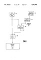
- FIG. 1 is an overall block diagram illustrating a memory system in which a memory word is stored on k separate chips each providing b bits to a computer memory system register;
- FIG. 2 is a functional block diagram illustrating the 15 possible error patterns for the case in which there are four bits per chip;
- FIGS. 3A and 3B are functional block diagrams illustrating the limits of error detectability for the circuits of the present invention.
- FIG. 4 is a general ECC (Error Correction Code) flow diagram, illustrating various staging registers and line buffers involved in the store and fetch operations for the present invention
- FIG. 5 is an illustration of the processing of bits during a data store operation
- FIG. 6 is a further illustration of the operation of a data store command according to the concepts presented by the present invention.
- FIG. 7 is an illustration of the processing of bits during a data fetch operation
- FIG. 8 is a further illustration of the operation of a data fetch command according to the concepts presented by the present invention.
- FIG. 9 illustrates the arrangement of data in memory modules on the SIMM array(s).
- the parity check matrix for this code including an embodiment utilizing two address parity bits is given below:
- each of the 12 ECC check bits is generated.
- the 12 ECC check bits are generated in two stages.
- a partial ECC check bit is generated by exclusive OR circuits which take a subset of 64 data bits as indicated by the 1's in each row of the parity check matrix in Table I.
- the first partial check bit is generated by exclusive-ORing data found at positions: 1, 5, 9, 13, 17, 21, 25, 29, 33, 36, 37, 38, 40, 41, 42, 43, 44, 47, 48, 49, 50, 53, 54, 57, 58, 59, 62 and 63.
- address parity bits are generated from selective combination of data from system address bits as discussed later in detail.
- the partial check bits are combined with the address parity bits and data bits to generate the final 12 ECC check bits.
- the set of 64 data bits together with the 12 check bits form an ECC word. Therefore, it seems that in the embodiment presented in Table I, when the two address parity bits are included, the ECC word is really a (78,66) code word. However, since the parity address bits have been used in the generation of the final 12 ECC check bits, it is unnecessary for them to be stored as part of the ECC word. Therefore, the code is still a (76,64) code since only 76 bits per code word are stored into the memory array or a SIMM (Single-Inline-Memory-Module) as shown in FIG. 9. The address parity bits are regenerated again during the fetch operation from incoming system address bits.
- SIMM Single-Inline-Memory-Module
- FIGS. 3A and 3B illustrate the limits of error detectability in the present invention.
- FIG. 3A particularly shows the situation in which chip i produces from one to four errors while only a single error occurs in chip J.
- Reference numeral 20 in FIGS. 1 through 3 refer to the individual memory chips.
- FIG. 3B illustrates the situation in which chip i produces from one to four errors while only a single error occurs in address parity.
- data bits are stored in a plurality of storage buffers.
- the 64 data bits are first stored in two storage buffers named STBUF - H - D(0 . . . 31) and STBUF - L - D(0 . . . 31), respectively.
- the address parity bits are located in address buffers indicated as STORE - ADDRP - D(0 . . . 1) in Table II above.
- the address parity bits are generated from selective combination of data from system address bits as shown in the example provided below in Table III.
- STORE - ADDRP - D(0) is generated from the parity of system address bits 1, 2, 5-14, 26, 27 and 30.
- STORE - ADDRP - D(1) is the parity of system address bits 0, 3, 4, 5-25, and 31.
- the mapping of system address bits to memory module depends on the size of the modules.
- the final ECC check bits are then generated by combining the contents of the STORE - ADDRP with the data stored in the storage buffers STBUF and the data obtained from the partial check bits generated from the Exclusive-Or circuitry.
- the partial check bits SY0(0 . . . 11) are generated from the high word data word STBUF - H - D(0 . . . 31) and SY1(0 . . . 11) are generated from the low data word STBUF - L - D(0 . . . 31).
- SY0 and SY1 and address parity bits are combined to produce the final check bits.
- the final 12 ECC check bits are stored in SEC - O - C(0 . . . 11) buffer.
- the following equation illustrates in detail the generation of the 12 ECC check bits and their final storage in the SEC - O - C(0 . . . 11) buffer.
- OPA (X
- the generation of check bits is divided in two stages as mentioned earlier.
- FIG. 4 is an illustration of the general ECC flow diagram.
- Logic steps 1 through 4, 100 through 400 are the various staging registers and line buffers used in the data store and data fetch operations.
- Logic steps 1 and 2, 100 and 200 involve different operations that finally allow the generation of ECC store operation 220 into the computer memory DRAM array 500. This information is later fetched from the DRAM array 500 to regenerate and decode the bits during the fetch operation, 300 through 400.
- FIG. 6 shows the storage of data in storage arrays 61, 62 and 63 before the generation of check bits 66,67 and 68.
- Table I above is an embodiment of the present invention utilizing two address parity bits. Other embodiments are conceivable, however, in accordance to the concepts of the present invention where the number of address parity bits, can either be reduced to one or increased to more than two. Table IV given below provides another embodiment of the present invention where eight address parity bits are generated and used.
- FIGS. 7 and 8 the reverse of the store process implemented during the store operation is used as shown in FIGS. 7 and 8.
- Data 70, 72 and 55, including the ECC word, is first fetched from memory 500, as shown in FIG. 7.
- FIG. 9 illustrates the circuits used during an ECC fetch operation.
- Data fetched from the DRAM array chips are named MDRMUX - H(0 . . . 31) 92 for modules 1 to 8, MDRMUX - L(0 . . . 31) 94 for modules 9 to 16 and MDRMUX - C(0 . . . 11) 96 for modules 17 to 19.
- a set of partial syndrome bits SYH(0 . . . 11) and SYL(0 . . . 11) is generated from the fetched data word from the DRAM array chips or the MDRMUX as illustrated in detail by the following equation:
- partial syndrome bit i is the Exclusive-OR of the fetched data word at positions specified by 1's in the ith row of the parity check matrix. That is to say that the partial syndrome bits are generated by supplying specified signals to a set of exclusive - OR gates.
- the syndrome bits SY(0 . . . 11) are then generated from the combination of the fetched data from check bits MDRMUX - C(0 . . . 11) and the address parity bits from Fetch - ADDRP(0 . . . m) generated from the incoming system address bits.
- the partial syndrome bits SY(0 . . . 11) 72 are then decoded 74 to identify any possible errors as illustrated in FIG. 7.
- Module error indicators are then generated according to the formula given below during the decoding process to detect and indicate errors.
- FIG. 8 illustrates a set of module errors indicators MOD - 00, MOD - 01, . . . MOD - 18 74. Any error will cause the setting of one of the MOD's. For example an error in module 0 will cause MOD - 00 to be set to 1.
- bit error indicators are also generated from circuit lines which are later used to invert the fetched data bits to correct certain errors. Invert lines 81 INV - H(0 . . . 31) 84, INV - L(0 . . . 31), and INV - C(0 . . . 11) are used in conjunction with bit errors so that when a bit error indicator is on, the corresponding data bit is corrected by inversion of the data.
- Bit error indicators 82 are generated from the following equations.
- the status of the module error and the syndromes are to enable a plurality of invert lines and generate other signals pertaining to types of errors 78 including a UE (Uncorrectable error) signal 79 or a CE (Correctable Error) signal 77.
- UE Uncorrectable error
- CE Correctable Error
- FIG. 9 illustrates the arrangement of data in the memory modules on the SIMMs.
- the data bits and check bits are divided into 4 bit symbols to store in 19 memory modules.
- SEC - O - H(0 . . . 31) are stored in modules 1 to 8
- SEC - 0 - L(0 . . . 31) are stored in modules 9 to 16
- SEC - 0 - C(0 . . . 11) are stored in modules 17 to 19.
- the mapping of system address bits to memory modules depends on the module size as shown in Table IV and FIG. 9.
Landscapes
- Engineering & Computer Science (AREA)
- Theoretical Computer Science (AREA)
- Quality & Reliability (AREA)
- Physics & Mathematics (AREA)
- General Engineering & Computer Science (AREA)
- General Physics & Mathematics (AREA)
- Detection And Correction Of Errors (AREA)
Abstract
Description
              TABLE I
______________________________________
=======================DATA=======================
1     2       3      4      5    6      7    8
====  ====    ====   ====   ==== ====   ==== ====
______________________________________
1000  1000    1000   1000   1000 1000   1000 1000
0100  0100    0100   0100   0100 0100   0100 0100
0010  0010    0010   0010   0010 0010   0010 0010
0001  0001    0001   0001   0001 0001   0001 0001
0110  1000    0010   1011   1010 1101   0101 1110
1101  0100    0001   0110   0101 1011   1111 1001
1011  0010    1010   1101   1000 0110   0100 1001
0110  0001    0101   1011   0100 1101   1100 0111
1000  1110    0111   1010   1001 0010   0110 0001
0100  1001    1110   0101   0111 0001   1101 0011
0010  1001    1110   1000   0111 1010   1011 0101
0001  0111    1001   0100   1110 0101   0110 1111
======================================================
______________________________________
=======================DATA=======================
9     10      11     12     13   14     15   16
====  ====    ====   ====   ==== ====   ==== ====
______________________________________
1001  1101    1111   0011   1100 1100   1110 0110
0111  1011    1010   0010   1000 1000   1001 1101
0111  0110    1100   1111   0011 0011   1001 1011
1110  1101    1000   1010   0010 0010   0111 0110
1000  0001    1000   0111   1000 1110   1000 0100
0100  0011    0100   1110   0100 1001   0100 1100
0010  0101    0010   1110   0010 1001   0010 0001
0001  1111    0001   1001   0001 0111   0001 0011
0101  1000    1011   1000   0110 1000   0100 1000
1111  0100    0110   0100   1101 0100   1100 0100
0100  0010    1101   0010   1011 0010   0001 0010
1100  0001    1011   0001   0110 0001   0011 0001
======================================================
______________________________________
====     ECC    ====      =======
                                 ADDRESS
                          SYMBOL PARITY
                          ID     BITS
17       18     19        (CHIP) 20
====     ====   ====      ID     ====
______________________________________
1000     0000   0000      --     01
0100     0000   0000      --     11
0010     0000   0000      --     10
0001     0000   0000      --     11
0000     1000   0000      --     10
0000     0100   0000      --     01
0000     0010   0000      --     00
0000     0001   0000      --     00
0000     0000   1000      --     00
0000     0000   0100      --     00
0000     0000   0010      --     01
0000     0000   0001      --     10
======================================================
______________________________________
              TABLE II
______________________________________
================= STBUF.sub.-- H.sub.-- D(0 . . . 31) =================
              11     1111  1111  2222  2222  2233
0123 4567    8901    2345  6789  0123  4567  8901
==== ====    ====    ====  ====  ====  ====  ====
______________________________________
1000 1000    1000    1000  1000  1000  1000  1000
0100 0100    0100    0100  0100  0100  0100  0100
0010 0010    0010    0010  0010  0010  0010  0010
0001 0001    0001    0001  0001  0001  0001  0001
0110 1000    0010    1011  1010  1101  0101  1110
1101 0100    0001    0110  0101  1011  1111  1001
1011 0010    1010    1101  1000  0110  0100  1001
0110 0001    0101    1011  0100  1101  1100  0111
1000 1110    0111    1010  1001  0010  0110  0001
0100 1001    1110    0101  0111  0001  1101  0011
0010 1001    1110    1000  0111  1010  1011  0101
0001 0111    1001    0100  1110  0101  0110  1111
======================================================
______________________________________
================= STBUF.sub.-- L.sub.-- D(0 . . . 31) =================
              11     1111  1111  2222  2222  2233
0123 4567    8901    2345  6789  0123  4567  8901
==== ====    ====    ====  ====  ====  ====  ====
______________________________________
1001 1101    1111    0011  1100  1100  1110  0110
0111 1011    1010    0010  1000  1000  1001  1101
0111 0110    1100    1111  0011  0011  1001  1011
1110 1101    1000    1010  0010  0010  0111  0110
1000 0001    1000    0111  1000  1110  1000  0100
0100 0011    0100    1110  0100  1001  0100  1100
0010 0101    0010    1110  0010  1001  0010  0001
0001 1111    0001    1001  0001  0111  0001  0011
0101 1000    1011    1000  0110  1000  0100  1000
1111 0100    0110    0100  1101  0100  1100  0100
0100 0010    1101    0010  1011  0010  0001  0010
1100 0001    1011    0001  0110  0001  0011  0001
======================================================
______________________________________
SEC.sub.-- O.sub.-- C(0 . . . 11)
                 11     STORE.sub.-- ADDRP.sub.-- D(0 . . . 1)
0123  4567      8901    01
====  ====      ====    ==
______________________________________
1000  0000      0000    01
0100  0000      0000    11
0010  0000      0000    10
0001  0000      0000    11
0000  1000      0000    10
0000  0100      0000    01
0000  0010      0000    00
0000  0001      0000    00
0000  0000      1000    00
0000  0000      0100    00
0000  0000      0010    01
0000  0000      0001    10
======================================================
______________________________________
                                  TABLE III
__________________________________________________________________________
 ##STR1##
 ##STR2##
 ##STR3##
 ##STR4##
 ##STR5##
 ##STR6##
 ##STR7##
 ##STR8##
 ##STR9##
 ##STR10##
 ##STR11##
__________________________________________________________________________
 CD means memory card selection bit
 C0-C11 means Column Address 0-11
 R0-R11 means Row Address 0-11
 EO means even/odd lines (on STC interleaving)
 RE means RAS A/B decode
__________________________________________________________________________
/********* STORE ECC **************************************************/
 ##STR12##
 ##STR13##
 ##STR14##
 ##STR15##
 ##STR16##
 ##STR17##
 ##STR18##
 ##STR19##
 ##STR20##
 ##STR21##
 ##STR22##
 ##STR23##
 ##STR24##
 ##STR25##
 ##STR26##
 ##STR27##
 ##STR28##
 ##STR29##
 ##STR30##
 ##STR31##
 ##STR32##
 ##STR33##
 ##STR34##
 ##STR35##
 ##STR36##
 ##STR37##
__________________________________________________________________________
              TABLE IV
______________________________________
=======================DATA=======================
1     2       3      4      5    6      7    8
====  ====    ====   ====   ==== ====   ==== ====
______________________________________
1000  1000    1000   1000   1000 1000   1000 1000
0100  0100    0100   0100   0100 0100   0100 0100
0010  0010    0010   0010   0010 0010   0010 0010
0001  0001    0001   0001   0001 0001   0001 0001
0110  1000    0010   1011   1010 1101   0101 1110
1101  0100    0001   0110   0101 1011   1111 1001
1011  0010    1010   1101   1000 0110   0100 1001
0110  0001    0101   1011   0100 1101   1100 0111
1000  1110    0111   1010   1001 0010   0110 0001
0100  1001    1110   0101   0111 0001   1101 0011
0010  1001    1110   1000   0111 1010   1011 0101
0001  0111    1001   0100   1110 0101   0110 1111
======================================================
______________________________________
=======================DATA=======================
9     10      11     12     13   14     15   16
====  ====    ====   ====   ==== ====   ==== ====
______________________________________
1001  1101    1111   0011   1100 1100   1110 0110
0111  1011    1010   0010   1000 1000   1001 1101
0111  0110    1100   1111   0011 0011   1001 1011
1110  1101    1000   1010   0010 0010   0111 0110
1000  0001    1000   0111   1000 1110   1000 0100
0100  0011    0100   1110   0100 1001   0100 1100
0010  0101    0010   1110   0010 1001   0010 0001
0001  1111    0001   1001   0001 0111   0001 0011
0101  1000    1011   1000   0110 1000   0100 1000
1111  0100    0110   0100   1101 0100   1100 0100
0100  0010    1101   0010   1011 0010   0001 0010
1100  0001    1011   0001   0110 0001   0011 0001
======================================================
______________________________________
====   ECC       ====   =======   ADDRESS
                        SYMBOL    PARITY
                        ID        BITS
17     18        19     (CHIP)    20   21
====   ====      ====   ID        ==== ====
______________________________________
1000   0000      0000   --        0111 1101
0100   0000      0000   --        1111 0010
0010   0000      0000   --        1011 0111
0001   0000      0000   --        1100 1101
0000   1000      0000   --        1000 0011
0000   0100      0000   --        0110 0111
0000   0010      0000   --        0001 0010
0000   0001      0000   --        0000 1110
0000   0000      1000   --        0000 1100
0000   0000      0100   --        0001 1010
0000   0000      0010   --        0110 1000
0000   0000      0001   --        1011 1001
======================================================
______________________________________
__________________________________________________________________________
 ##STR38##
 ##STR39##
 ##STR40##
 ##STR41##
 ##STR42##
 ##STR43##
 ##STR44##
 ##STR45##
 ##STR46##
 ##STR47##
 ##STR48##
 ##STR49##
 ##STR50##
__________________________________________________________________________
__________________________________________________________________________
/*********************Syndrome Generation****************************/
SY(0):=
MDRMUX.sub.-- C(0)XOR SYH(0)XOR SYL(0)XOR FETCH.sub.-- ADDRP(1);
SY(1):=
MDRMUX.sub.-- C(1)XOR SYH(1)XOR SYL(1)
XOR FETCH.sub.-- ADDRP(0)XOR FETCH.sub.-- ADDRP(1);
SY(2):=
MDRMUX.sub.-- C(2)XOR SYH(2)XOR SYL(2) XOR FETCH.sub.-- ADDRP(0);
SY(3):=
MDRMUX.sub.-- C(3)XOR SYH(3)XOR SYL(3)
XOR FETCH.sub.-- ADDRP(0)XOR FETCH.sub.-- ADDRP(1);
SY(4):=
MDRMUX.sub.-- C(4)XOR SYH(4)XOR SYL(4) XOR FETCH.sub.-- ADDRP(0);
SY(5):=
MDRMUX.sub.-- C(5)XOR SYH(5)XOR SYL(5)XOR FETCH.sub.-- ADDRP(1);
SY(6):=
MDRMUX.sub.-- C(6)XOR SYH(6)XOR SYL(6);
SY(7):=
MDRMUX.sub.-- C(7)XOR SYH(7)XOR SYL(7);
SY(8):=
MDRMUX.sub.-- C(8)XOR SYH(8)XOR SYL(8);
SY(9):=
MDRMUX.sub.-- C(9)XOR SYH(9)XOR SYL(9);
SY(10):=
MDRMUX.sub.-- C(10)XOR SYH(10)XOR SYL(10)XOR FETCH.sub.-- ADDRP(1);
SY(11):=
MDRMUX.sub.-- C(11)XOR SYH(11)XOR SYL(11) XOR FETCH.sub.-- ADDRP(0);
__________________________________________________________________________
__________________________________________________________________________
/* **** Syndrome & Module Decoding ***********************************/
/*
*/ /* MOD.sub.-- 00 means: The most left Module 0 is defective
MOD.sub.-- 00: =
( SY(1)
XOR
SY(2) XOR
SY(4)
)
&(
SY(0)
XOR
SY(1) XOR
SY(3)
XOR
SY(5)
)
&(
SY(0) XOR
SY(2)
XOR
SY(3)
XOR
SY(6)
)
&( SY(1)
XOR
SY(2) XOR
SY(7)
)
&(
SY(0) XOR
SY(8)
)
&( SY(1) XOR
SY(9)
)
&( SY(2) XOR
SY(10)
)
&( SY(3)
XOR
SY(11)
);
MOD.sub.-- 01: =
( SY(0) XOR
SY(4)
)
&( SY(1) XOR
SY(5)
)
&( SY(2) XOR
SY(6)
)
&( SY(3)
XOR
SY(7)
)
&(
SY(0)
XOR
SY(1)
XOR
SY(2) XOR
SY(8)
)
&(
SY(0) XOR
SY(3)
XOR
SY(9)
)
&(
SY(0) XOR
SY(3)
XOR
SY(10)
)
&( SY(1)
XOR
SY(2)
XOR
SY(3)
XOR
SY(11)
);
MOD.sub.-- 02: =
( SY(2) XOR
SY(4)
)
&( SY(3)
XOR
SY(5)
)
&(
SY(0) XOR
SY(2) XOR
SY(6)
)
&( SY(1) XOR
SY(3)
XOR
SY(7)
)
&( SY(1)
XOR
SY(2)
XOR
SY(3)
XOR
(8) )
&(
SY(0)
XOR
SY(1)
XOR
SY(2) XOR
SY(9)
)
&(
SY(0)
XOR
SY(1)
XOR
SY(2) XOR
SY(10)
)
&(
SY(0) XOR
SY(3)
XOR
SY(11)
);
MOD.sub.-- 03: =
( SY(0) XOR
SY(2)
XOR
SY(3)
XOR
SY(4)
)
&( SY(1)
XOR
SY(2) XOR
SY(5)
)
&(
SY(0)
XOR
SY(1) XOR
SY(3)
XOR
SY(6)
)
&(
SY(0) XOR
SY(2)
XOR
SY(3)
XOR
SY(7)
)
&(
SY(0) XOR
SY(2) XOR
SY(8)
)
&( SY(1) XOR
SY(3)
XOR
SY(9)
)
&(
SY(0) XOR
SY(10)
)
&( SY(1) XOR
SY(11)
);
MOD.sub.-- 04: =
( SY(0) XOR
SY(2) XOR
SY(4)
);
&( SY(1) XOR
SY(3)
XOR
SY(5)
)
&(
SY(0) XOR
SY(6)
)
&( SY(1) XOR
SY(7)
)
&(
SY(0) XOR
SY(3)
XOR
SY(8)
)
&( SY(1)
XOR
SY(2)
XOR
SY(3)
XOR
SY(9)
)
&( SY(1)
XOR
SY(2)
XOR
SY(3)
XOR
SY(10)
)
&(
SY(0)
XOR
SY(1)
XOR
SY(2) XOR
SY(11)
);
MOD.sub.-- 05: =
( SY(0)
XOR
SY(1) XOR
SY(3)
XOR
SY(4)
)
&(
SY(0) XOR
SY(2)
XOR
SY(3)
XOR
SY(5)
)
&( SY(1)
XOR
SY(2) XOR
SY(6)
)
&(
SY(0)
XOR
SY(1) XOR
SY(3)
XOR
SY(7)
)
&( SY(2) XOR
SY(8)
)
&( SY(3)
XOR
SY(9)
)
&(
SY(0) XOR
SY(2) XOR
SY(10)
)
&( SY(1) XOR
SY(3)
XOR
SY(11)
);
MOD.sub.-- 06: =
( SY(1) XOR
SY(3)
XOR
SY(4)
)
&(
SY(0)
XOR
SY(1)
XOR
SY(2)
XOR
SY(3)
XOR
SY(5)
)
&( SY(1) XOR
SY(6)
)
&(
SY(0)
XOR
SY(1) XOR
SY(7)
)
&( SY(1)
XOR
SY(2) XOR
SY(8)
)
&(
SY(0)
XOR
SY(1) XOR
SY(3)
XOR
SY(9)
)
&(
SY(0) XOR
SY(2)
XOR
SY(3)
XOR
SY(10)
)
&( SY(1)
XOR
SY(2) XOR
SY(11)
);
MOD.sub.-- 07: =
( SY(0)
XOR
SY(1)
XOR
SY(2) XOR
SY(4)
)
&(
SY(0) XOR
SY(3)
XOR
SY(5)
)
&(
SY(0) XOR
SY(3)
XOR
SY(6)
)
&( SY(1)
XOR
SY(2)
XOR
SY(3)
XOR
SY(7)
)
&( SY(3)
XOR
SY(8)
)
&( SY(2)
XOR
SY(3)
XOR
SY(9)
)
&( SY(1) XOR
SY(3)
XOR
SY(10)
)
&(
SY(0)
XOR
SY(1)
XOR
SY(2)
XOR
SY(3)
XOR
SY(11)
);
MOD.sub.-- 08: =
( (SY(4) XOR
SY(7)
XOR
SY(0)
)
&( SY(5)
XOR
SY(6)
XOR
SY(7)
XOR
SY(1)
)
&( SY(5)
XOR
SY(6)
XOR
SY(7)
XOR
SY(2)
)
&(
SY(4)
XOR
SY(5)
XOR
SY(6) XOR
SY(3)
)
&( SY(5) XOR
SY(7)
XOR
SY(8)
)
&(
SY(4)
XOR
SY(5)
XOR
SY(6)
XOR
SY(7)
XOR
SY(9)
)
&( SY(5) XOR
SY(10)
)
&(
SY(4)
XOR
SY(5) XOR
SY(11)
);
MOD.sub.-- 09: =
( SY(8)
XOR
SY(9) XOR
SY(11)
XOR
SY(0)
)
&(
SY(8) XOR
SY(10)
XOR
SY(11)
XOR
SY(1)
)
&( SY(9)
XOR
SY(10) XOR
SY(2)
)
&(
SY(8)
XOR
SY(9) XOR
SY(11)
XOR
SY(3)
)
&( SY(11)
XOR
SY(4)
)
&( SY(10)
XOR
SY(11)
XOR
SY(5)
)
&( SY(9) XOR
SY(11)
XOR
SY(6)
)
&(
SY(8)
XOR
SY(9)
XOR
SY(10)
XOR
SY(11)
XOR
SY(7)
);
MOD.sub.-- 10: =
( SY(4)
XOR
SY(5)
XOR
SY(6)
XOR
SY(7)
XOR
SY(0)
)
&(
SY(4) XOR
SY(6) XOR
SY(1)
)
&(
SY(4)
XOR
SY(5) XOR
SY(2)
)
&(
SY(4) XOR
SY(3)
)
&(
SY(4) XOR
SY(6)
XOR
SY(7)
XOR
SY(8)
)
&( SY(5)
XOR
SY(6) XOR
SY(9)
)
&(
SY(4)
XOR
SY(5) XOR
SY(7)
XOR
SY(10)
)
&(
SY(4) XOR
SY(6)
XOR
SY(7)
XOR
SY(11)
);
MOD.sub.-- 11: =
( SY(10)
XOR
SY(11)
XOR
SY(0)
)
&( SY(10) XOR
SY(1)
)
&(
SY(8)
XOR
SY(9)
XOR
SY(10)
XOR
SY(11)
XOR
SY(2)
)
&(
SY(8) XOR
SY(10) XOR
SY(3)
)
&( SY(9)
XOR
SY(10)
XOR
SY(11)
XOR
SY(4)
)
&(
SY(8)
XOR
SY(9)
XOR
SY(10) XOR
SY(5)
)
&(
SY(8)
XOR
SY(9)
XOR
SY(10) XOR
SY(6)
)
&(
SY(8) XOR
SY(11)
XOR
SY(7)
);
MOD.sub.-- 12: =
( SY(4)
XOR
SY(5) XOR
SY(0)
)
&(
SY(4) XOR
SY(1)
)
&( SY(6)
XOR
SY(7)
XOR
SY(2)
)
&( SY(6) XOR
SY(3)
)
&( SY(5)
XOR
SY(6) XOR
SY(8)
)
&(
SY(4)
XOR
SY(5) XOR
SY(7)
XOR
SY(9)
)
&(
SY(4) XOR
SY(6)
XOR
SY(7)
XOR
SY(10)
)
&( SY(5)
XOR
SY(6) XOR
SY(11)
);
MOD.sub.-- 13: =
( SY(8)
XOR
SY(9) XOR
SY(0)
)
&(
SY(8) XOR
SY(1)
)
&( SY(10)
XOR
SY(11)
XOR
SY(2)
)
&( SY(10) XOR
SY(3)
)
&(
SY(8)
XOR
SY(9)
XOR
SY(10) XOR
SY(4)
)
&(
SY(8) XOR
SY(11)
XOR
SY(5)
)
&(
SY(8) XOR
SY(11)
XOR
SY(6)
)
&( SY(9)
XOR
SY(10)
XOR
SY(11)
XOR
SY(7)
);
MOD.sub.-- 14: =
( SY(4)
XOR
SY(5)
XOR
SY(6) XOR
SY(0)
)
&(
SY(4) XOR
SY(7)
XOR
SY(1)
)
&(
SY(4) XOR
SY(7)
XOR
SY(2)
)
&( SY(5)
XOR
SY(6)
XOR
SY(7)
XOR
SY(3)
)
&( SY(5) XOR
SY(8)
)
&(
SY(4)
XOR
SY(5) XOR
SY(9)
)
&( SY(7)
XOR
SY(10)
)
&( SY(6)
XOR
SY(7)
XOR
SY(11)
);
MOD.sub.-- 15: =
( SY(9)
XOR
SY(10) XOR
SY(0)
)
&(
SY(8)
XOR
SY(9) XOR
SY(11)
XOR
SY(1)
)
&(
SY(8) XOR
SY(10)
XOR
SY(11)
XOR
SY(2)
)
&( SY(9)
XOR
SY(10) XOR
SY(3)
)
&( SY(9) XOR
SY(4)
)
&(
SY(8)
XOR
SY(9) XOR
SY(5)
)
&( SY(11)
XOR
SY(6)
)
&( SY(10)
XOR
SY(11)
XOR
SY(7)
);
MOD.sub.-- 16: =
( SY(4)
)
&( SY(5)
)
&( SY(6)
)
&( SY(7)
)
&( SY(8)
)
&( SY(9)
)
&( SY(10)
)
&( SY(11)
);
MOD.sub.-- 17: =
( SY(0)
)
&( SY(0)
)
&( SY(1)
)
&( SY(2)
)
&( SY(3)
)
&( SY(8)
)
&( SY(9)
)
&( SY(10)
)
&( SY(11)
);
MOD.sub.-- 18: =
( SY(0)
)
&( SY(1)
)
&( SY(2)
)
&( SY(3)
)
&( SY(4)
)
&( SY(5)
)
&( SY(6)
)
&( SY(7)
);
__________________________________________________________________________
______________________________________
/***********Invert Enabling********************************/
INV.sub.-- H(0 . . . 3):=MOD.sub.-- 00GATESY(0 . . . 3);
INV.sub.-- H(4 . . . 7):=MOD.sub.-- 01GATESY(0 . . . 3);
INV.sub.-- H(8 . . . 11):=MOD.sub.-- 02GATESY(0 . . . 3);
INV.sub.-- H(12 . . . 15):=MOD.sub.-- 03GATESY(0 . . . 3);
INV.sub.-- H(16 . . . 19):=MOD.sub.-- 04GATESY(0 . . . 3);
INV.sub.-- H(20 . . . 23):=MOD.sub.-- 05GATESY(0 . . . 3);
INV.sub.-- H(24 . . . 27):=MOD.sub.-- 06GATESY(0 . . . 3);
INV.sub.-- H(28 . . . 31):=MOD.sub.-- 07GATESY(0 . . . 3);
INV.sub.-- L(0 . . . 3):=MOD.sub.-- 08GATESY(4 . . . 7);
INV.sub.-- L(4 . . . 7):=MOD.sub.-- 09GATESY(8 . . . 11);
INV.sub.-- L(8 . . . 11):=MOD.sub.-- 10GATESY(4 . . . 7);
INV.sub.-- L(12 . . . 15):=MOD.sub.-- 11GATESY(8 . . . 11);
INV.sub.-- L(16 . . . 19):=MOD.sub.-- 12GATESY(4 . . . 7);
INV.sub.-- L(20 . . . 23):=MOD.sub.-- 13GATESY(8 . . . 11);
INV.sub.-- L(24 . . . 27):=MOD.sub.-- 14GATESY(4 . . . 7);
INV.sub.-- L(28 . . . 31):=MOD.sub.-- 15GATESY(8 . . . 11);
INV.sub.-- C(0 . . . 3):=MOD.sub.-- 16GATESY(0 . . . 3);
INV.sub.-- C(4 . . . 7):=MOD.sub.-- 17GATESY(4 . . . 7);
INV.sub.-- C(8 . . . 11):=MOD.sub.-- 18GATESY(8 . . . 11);
______________________________________
__________________________________________________________________________
/****************Error Indication***********************************/
 ##STR51##
 ##STR52##
ECC.sub.-- UCE:= ECC.sub.-- ANYE &   ECC.sub.-- CE;
/*************************************************************************
****/ /*>
INVERTAND FETCH.sub.-- ECC.sub.-- OUTPUT<*/
/*************************************************************************
****/
STEP3.sub.-- IN.sub.-- H(0 . . . 31) := MDRMUX.sub.-- OUT.sub.-- H(0 . .
. 31) XOR INV.sub.-- H(0 . . . 31);
STEP3.sub.-- IN.sub.-- L(0 . . . 31) := MDRMUX.sub.-- OUT.sub.-- L(0 . .
. 31) XOR INV.sub.-- L(0 . . . 31);
STEP3.sub.-- IN.sub.-- C(0 . . . 11) := MDRMUX.sub.-- OUT.sub.-- C(0 . .
. 11) XOR INV.sub.-- C(0 . . . 11);
__________________________________________________________________________
Claims (2)
______________________________________
=======================DATA=======================
1     2       3      4      5    6      7    8
====  ====    ====   ====   ==== ====   ==== ====
______________________________________
1000  1000    1000   1000   1000 1000   1000 1000
0100  0100    0100   0100   0100 0100   0100 0100
0010  0010    0010   0010   0010 0010   0010 0010
0001  0001    0001   0001   0001 0001   0001 0001
0110  1000    0010   1011   1010 1101   0101 1110
1101  0100    0001   0110   0101 1011   1111 1001
1011  0010    1010   1101   1000 0110   0100 1001
0110  0001    0101   1011   0100 1101   1100 0111
1000  1110    0111   1010   1001 0010   0110 0001
0100  1001    1110   0101   0111 0001   1101 0011
0010  1001    1110   1000   0111 1010   1011 0101
0001  0111    1001   0100   1110 0101   0110 1111
======================================================
______________________________________
=======================DATA=======================
9     10      11     12     13   14     15   16
====  ====    ====   ====   ==== ====   ==== ====
______________________________________
1001  1101    1111   0011   1100 1100   1110 0110
0111  1011    1010   0010   1000 1000   1001 1101
0111  0110    1100   1111   0011 0011   1001 1011
1110  1101    1000   1010   0010 0010   0111 0110
1000  0001    1000   0111   1000 1110   1000 0100
0100  0011    0100   1110   0100 1001   0100 1100
0010  0101    0010   1110   0010 1001   0010 0001
0001  1111    0001   1001   0001 0111   0001 0011
0101  1000    1011   1000   0110 1000   0100 1000
1111  0100    0110   0100   1101 0100   1100 0100
0100  0010    1101   0010   1011 0010   0001 0010
1100  0001    1011   0001   0110 0001   0011 0001
======================================================
______________________________________
====     ECC    ====      =======
                                 ADDRESS
                          SYMBOL PARITY
                          ID     BITS
17       18     19        (CHIP) 20
====     ====   ====      ID     ====
______________________________________
1000     0000   0000      --     01
0100     0000   0000      --     11
0010     0000   0000      --     10
0001     0000   0000      --     11
0000     1000   0000      --     10
0000     0100   0000      --     01
0000     0010   0000      --     00
0000     0001   0000      --     00
0000     0000   1000      --     00
0000     0000   0100      --     00
0000     0000   0010      --     01
0000     0000   0001      --     10
======================================================
______________________________________
______________________________________
=======================DATA=======================
1     2       3      4      5    6      7    8
====  ====    ====   ====   ==== ====   ==== ====
______________________________________
1000  1000    1000   1000   1000 1000   1000 1000
0100  0100    0100   0100   0100 0100   0100 0100
0010  0010    0010   0010   0010 0010   0010 0010
0001  0001    0001   0001   0001 0001   0001 0001
0110  1000    0010   1011   1010 1101   0101 1110
1101  0100    0001   0110   0101 1011   1111 1001
1011  0010    1010   1101   1000 0110   0100 1001
0110  0001    0101   1011   0100 1101   1100 0111
1000  1110    0111   1010   1001 0010   0110 0001
0100  1001    1110   0101   0111 0001   1101 0011
0010  1001    1110   1000   0111 1010   1011 0101
0001  0111    1001   0100   1110 0101   0110 1111
======================================================
______________________________________
=======================DATA=======================
9     10      11     12     13   14     15   16
====  ====    ====   ====   ==== ====   ==== ====
______________________________________
1001  1101    1111   0011   1100 1100   1110 0110
0111  1011    1010   0010   1000 1000   1001 1101
0111  0110    1100   1111   0011 0011   1001 1011
1110  1101    1000   1010   0010 0010   0111 0110
1000  0001    1000   0111   1000 1110   1000 0100
0100  0011    0100   1110   0100 1001   0100 1100
0010  0101    0010   1110   0010 1001   0010 0001
0001  1111    0001   1001   0001 0111   0001 0011
0101  1000    1011   1000   0110 1000   0100 1000
1111  0100    0110   0100   1101 0100   1100 0100
0100  0010    1101   0010   1011 0010   0001 0010
1100  0001    1011   0001   0110 0001   0011 0001
======================================================
______________________________________
====   ECC       ====   =======   ADDRESS
                        SYMBOL    PARITY
                        ID        BITS
17     18        19     (CHIP)    20   21
====   ====      ====   ID        ==== ====
______________________________________
1000   0000      0000   --        0111 1101
0100   0000      0000   --        1111 0010
0010   0000      0000   --        1011 0111
0001   0000      0000   --        1100 1101
0000   1000      0000   --        1000 0011
0000   0100      0000   --        0110 0111
0000   0010      0000   --        0001 0010
0000   0001      0000   --        0000 1110
0000   0000      1000   --        0000 1100
0000   0000      0100   --        0001 1010
0000   0000      0010   --        0110 1000
0000   0000      0001   --        1011 1001
======================================================
______________________________________
Priority Applications (2)
| Application Number | Priority Date | Filing Date | Title |
|---|---|---|---|
| US08/570,446 US5691996A (en) | 1995-12-11 | 1995-12-11 | Memory implemented error detection and correction code with address parity bits |
| US08/824,098 US5751745A (en) | 1995-12-11 | 1997-03-25 | Memory implemented error detection and correction code with address parity bits |
Applications Claiming Priority (1)
| Application Number | Priority Date | Filing Date | Title |
|---|---|---|---|
| US08/570,446 US5691996A (en) | 1995-12-11 | 1995-12-11 | Memory implemented error detection and correction code with address parity bits |
Related Child Applications (1)
| Application Number | Title | Priority Date | Filing Date |
|---|---|---|---|
| US08/824,098 Division US5751745A (en) | 1995-12-11 | 1997-03-25 | Memory implemented error detection and correction code with address parity bits |
Publications (1)
| Publication Number | Publication Date |
|---|---|
| US5691996A true US5691996A (en) | 1997-11-25 |
Family
ID=24279678
Family Applications (2)
| Application Number | Title | Priority Date | Filing Date |
|---|---|---|---|
| US08/570,446 Expired - Fee Related US5691996A (en) | 1995-12-11 | 1995-12-11 | Memory implemented error detection and correction code with address parity bits |
| US08/824,098 Expired - Fee Related US5751745A (en) | 1995-12-11 | 1997-03-25 | Memory implemented error detection and correction code with address parity bits |
Family Applications After (1)
| Application Number | Title | Priority Date | Filing Date |
|---|---|---|---|
| US08/824,098 Expired - Fee Related US5751745A (en) | 1995-12-11 | 1997-03-25 | Memory implemented error detection and correction code with address parity bits |
Country Status (1)
| Country | Link |
|---|---|
| US (2) | US5691996A (en) |
Cited By (12)
| Publication number | Priority date | Publication date | Assignee | Title |
|---|---|---|---|---|
| US5841795A (en) * | 1996-02-12 | 1998-11-24 | Compaq Computer Corporation | Error correction codes |
| US5978953A (en) * | 1996-12-19 | 1999-11-02 | Compaq Computer Corporation | error detection and correction |
| US6003144A (en) * | 1997-06-30 | 1999-12-14 | Compaq Computer Corporation | Error detection and correction |
| US6024486A (en) * | 1996-06-05 | 2000-02-15 | Compaq Computer Corporation | Data error detection and correction |
| US6751769B2 (en) * | 2000-06-06 | 2004-06-15 | International Business Machines Corporation | (146,130) error correction code utilizing address information |
| US20060077750A1 (en) * | 2004-10-07 | 2006-04-13 | Dell Products L.P. | System and method for error detection in a redundant memory system |
| US7203890B1 (en) | 2004-06-16 | 2007-04-10 | Azul Systems, Inc. | Address error detection by merging a polynomial-based CRC code of address bits with two nibbles of data or data ECC bits |
| US20070255999A1 (en) * | 2006-04-07 | 2007-11-01 | Qimonda Ag | Memory Arrangement And Method For Error Correction |
| US7398449B1 (en) * | 2004-06-16 | 2008-07-08 | Azul Systems, Inc. | Encoding 64-bit data nibble error correct and cyclic-redundancy code (CRC) address error detect for use on a 76-bit memory module |
| US7426678B1 (en) * | 2004-07-20 | 2008-09-16 | Xilinx, Inc. | Error checking parity and syndrome of a block of data with relocated parity bits |
| US7506226B2 (en) | 2006-05-23 | 2009-03-17 | Micron Technology, Inc. | System and method for more efficiently using error correction codes to facilitate memory device testing |
| US20130080854A1 (en) * | 2011-09-23 | 2013-03-28 | International Business Machines Corporation | Address error detection |
Families Citing this family (6)
| Publication number | Priority date | Publication date | Assignee | Title |
|---|---|---|---|---|
| EP0922254B1 (en) * | 1996-08-30 | 2000-05-24 | Siemens Aktiengesellschaft | Error recognition in a storage system |
| JP4747332B2 (en) * | 2001-06-27 | 2011-08-17 | 独立行政法人 日本原子力研究開発機構 | Photon, radiation and neutron detectors and image detectors using superconducting tunnel junction elements |
| US7058881B2 (en) * | 2002-03-15 | 2006-06-06 | Broadcom Corporation | Distributed 4-bits diagonal interleaved parity (DIP4) checker |
| EP1394559A1 (en) * | 2002-08-27 | 2004-03-03 | Siemens Aktiengesellschaft | Method and apparatus for wire fault detection and correction |
| US7191388B1 (en) * | 2004-03-01 | 2007-03-13 | Lattice Semiconductor Corporation | Fast diagonal interleaved parity (DIP) calculator |
| US20060156191A1 (en) * | 2005-01-07 | 2006-07-13 | Steve Driediger | Memory addressing error protection systems and methods |
Citations (6)
| Publication number | Priority date | Publication date | Assignee | Title |
|---|---|---|---|---|
| US4862463A (en) * | 1987-07-20 | 1989-08-29 | International Business Machines Corp. | Error correcting code for 8-bit-per-chip memory with reduced redundancy |
| US5058115A (en) * | 1989-03-10 | 1991-10-15 | International Business Machines Corp. | Fault tolerant computer memory systems and components employing dual level error correction and detection with lock-up feature |
| US5070504A (en) * | 1989-06-23 | 1991-12-03 | International Business Machines | Method and apparatus for providing error correction to symbol level codes |
| US5161163A (en) * | 1989-06-23 | 1992-11-03 | International Business Machines Corporation | Method and apparatus for providing error correction to symbol level codes |
| US5228046A (en) * | 1989-03-10 | 1993-07-13 | International Business Machines | Fault tolerant computer memory systems and components employing dual level error correction and detection with disablement feature |
| US5345582A (en) * | 1991-12-20 | 1994-09-06 | Unisys Corporation | Failure detection for instruction processor associative cache memories |
Family Cites Families (4)
| Publication number | Priority date | Publication date | Assignee | Title |
|---|---|---|---|---|
| US3531631A (en) * | 1967-01-11 | 1970-09-29 | Ibm | Parity checking system |
| US3555255A (en) * | 1968-08-09 | 1971-01-12 | Bell Telephone Labor Inc | Error detection arrangement for data processing register |
| US4443876A (en) * | 1981-08-31 | 1984-04-17 | Bell Telephone Laboratories, Incorporated | Fast parity generation for find low order zero circuit |
| JPS61109155A (en) * | 1984-11-01 | 1986-05-27 | Mitsubishi Electric Corp | Parity detection circuit |
-
1995
- 1995-12-11 US US08/570,446 patent/US5691996A/en not_active Expired - Fee Related
-
1997
- 1997-03-25 US US08/824,098 patent/US5751745A/en not_active Expired - Fee Related
Patent Citations (6)
| Publication number | Priority date | Publication date | Assignee | Title |
|---|---|---|---|---|
| US4862463A (en) * | 1987-07-20 | 1989-08-29 | International Business Machines Corp. | Error correcting code for 8-bit-per-chip memory with reduced redundancy |
| US5058115A (en) * | 1989-03-10 | 1991-10-15 | International Business Machines Corp. | Fault tolerant computer memory systems and components employing dual level error correction and detection with lock-up feature |
| US5228046A (en) * | 1989-03-10 | 1993-07-13 | International Business Machines | Fault tolerant computer memory systems and components employing dual level error correction and detection with disablement feature |
| US5070504A (en) * | 1989-06-23 | 1991-12-03 | International Business Machines | Method and apparatus for providing error correction to symbol level codes |
| US5161163A (en) * | 1989-06-23 | 1992-11-03 | International Business Machines Corporation | Method and apparatus for providing error correction to symbol level codes |
| US5345582A (en) * | 1991-12-20 | 1994-09-06 | Unisys Corporation | Failure detection for instruction processor associative cache memories |
Non-Patent Citations (2)
| Title |
|---|
| Norbert Schumacher, Memory Controller Design in VLSI and Computer Peripheals, 1 38 1 42 1989. * |
| Norbert Schumacher, Memory Controller Design in VLSI and Computer Peripheals, 1-38-1-42 1989. |
Cited By (21)
| Publication number | Priority date | Publication date | Assignee | Title |
|---|---|---|---|---|
| US5841795A (en) * | 1996-02-12 | 1998-11-24 | Compaq Computer Corporation | Error correction codes |
| US6024486A (en) * | 1996-06-05 | 2000-02-15 | Compaq Computer Corporation | Data error detection and correction |
| US5978953A (en) * | 1996-12-19 | 1999-11-02 | Compaq Computer Corporation | error detection and correction |
| US6003144A (en) * | 1997-06-30 | 1999-12-14 | Compaq Computer Corporation | Error detection and correction |
| US6751769B2 (en) * | 2000-06-06 | 2004-06-15 | International Business Machines Corporation | (146,130) error correction code utilizing address information |
| US20080235558A1 (en) * | 2004-06-16 | 2008-09-25 | Azul Systems, Inc. | Subsystem and Method for Encoding 64-bit Data Nibble Error Correct and Cyclic-Redundancy Code (CRC) Address Error Detect for Use in a 76-bit Memory Module |
| US7203890B1 (en) | 2004-06-16 | 2007-04-10 | Azul Systems, Inc. | Address error detection by merging a polynomial-based CRC code of address bits with two nibbles of data or data ECC bits |
| US8099651B2 (en) * | 2004-06-16 | 2012-01-17 | Azul Systems, Inc. | Subsystem and method for encoding 64-bit data nibble error correct and cyclic-redundancy code (CRC) address error detect for use in a 76-bit memory module |
| US7398449B1 (en) * | 2004-06-16 | 2008-07-08 | Azul Systems, Inc. | Encoding 64-bit data nibble error correct and cyclic-redundancy code (CRC) address error detect for use on a 76-bit memory module |
| US8245102B1 (en) * | 2004-07-20 | 2012-08-14 | Xilinx, Inc. | Error checking parity and syndrome of a block of data with relocated parity bits |
| US7426678B1 (en) * | 2004-07-20 | 2008-09-16 | Xilinx, Inc. | Error checking parity and syndrome of a block of data with relocated parity bits |
| US7895509B1 (en) | 2004-07-20 | 2011-02-22 | Xilinx, Inc. | Error checking parity and syndrome of a block of data with relocated parity bits |
| US8301988B1 (en) | 2004-07-20 | 2012-10-30 | Xilinx, Inc. | Error checking parity and syndrome of a block of data with relocated parity bits |
| US20090187806A1 (en) * | 2004-10-07 | 2009-07-23 | Dell Products L.P. | System and method for error detection in a redundant memory system |
| US20060077750A1 (en) * | 2004-10-07 | 2006-04-13 | Dell Products L.P. | System and method for error detection in a redundant memory system |
| US8341499B2 (en) * | 2004-10-07 | 2012-12-25 | Dell Products L.P. | System and method for error detection in a redundant memory system |
| US20070255999A1 (en) * | 2006-04-07 | 2007-11-01 | Qimonda Ag | Memory Arrangement And Method For Error Correction |
| US7506226B2 (en) | 2006-05-23 | 2009-03-17 | Micron Technology, Inc. | System and method for more efficiently using error correction codes to facilitate memory device testing |
| US20130080854A1 (en) * | 2011-09-23 | 2013-03-28 | International Business Machines Corporation | Address error detection |
| US8949694B2 (en) * | 2011-09-23 | 2015-02-03 | International Business Machines Corporation | Address error detection |
| US9208027B2 (en) | 2011-09-23 | 2015-12-08 | International Business Machines Corporation | Address error detection |
Also Published As
| Publication number | Publication date |
|---|---|
| US5751745A (en) | 1998-05-12 |
Similar Documents
| Publication | Publication Date | Title |
|---|---|---|
| US5768294A (en) | Memory implemented error detection and correction code capable of detecting errors in fetching data from a wrong address | |
| US5691996A (en) | Memory implemented error detection and correction code with address parity bits | |
| EP0535086B1 (en) | Multiple error correction in a computer memory | |
| US6018817A (en) | Error correcting code retrofit method and apparatus for multiple memory configurations | |
| US5313475A (en) | ECC function with self-contained high performance partial write or read/modify/write and parity look-ahead interface scheme | |
| US6751769B2 (en) | (146,130) error correction code utilizing address information | |
| US4345328A (en) | ECC Check bit generation using through checking parity bits | |
| US6044483A (en) | Error propagation operating mode for error correcting code retrofit apparatus | |
| EP1204921B1 (en) | System and method for detecting double-bit errors and for correcting errors due to component failures | |
| EP1183605B1 (en) | System and method for protecting data and correcting bit errors due to component failures | |
| US6662333B1 (en) | Shared error correction for memory design | |
| US5745508A (en) | Error-detection code | |
| US4740968A (en) | ECC circuit failure detector/quick word verifier | |
| US6442726B1 (en) | Error recognition in a storage system | |
| JPH087721B2 (en) | Data processing system having error detection / correction mechanism | |
| US5761221A (en) | Memory implemented error detection and correction code using memory modules | |
| JPS6115238A (en) | Correction of errors | |
| EP0668561A2 (en) | A flexible ECC/parity bit architecture | |
| JPS6047625B2 (en) | error correction system | |
| US4689792A (en) | Self test semiconductor memory with error correction capability | |
| US4631725A (en) | Error correcting and detecting system | |
| US4236247A (en) | Apparatus for correcting multiple errors in data words read from a memory | |
| US6393597B1 (en) | Mechanism for decoding linearly-shifted codes to facilitate correction of bit errors due to component failures | |
| US6463563B1 (en) | Single symbol correction double symbol detection code employing a modular H-matrix | |
| US6460157B1 (en) | Method system and program products for error correction code conversion |
Legal Events
| Date | Code | Title | Description |
|---|---|---|---|
| AS | Assignment |
Owner name: INTERNATIONAL BUSINESS MACHINES CORPORATION, NEW Y Free format text: ASSIGNMENT OF ASSIGNORS INTEREST;ASSIGNORS:CHEN, C. L.;HSIAO, M. Y.;LIPPONER, W. H.;AND OTHERS;REEL/FRAME:007840/0566;SIGNING DATES FROM 19951211 TO 19960110 |
|
| FEPP | Fee payment procedure |
Free format text: PAYER NUMBER DE-ASSIGNED (ORIGINAL EVENT CODE: RMPN); ENTITY STATUS OF PATENT OWNER: LARGE ENTITY |
|
| FEPP | Fee payment procedure |
Free format text: PAYOR NUMBER ASSIGNED (ORIGINAL EVENT CODE: ASPN); ENTITY STATUS OF PATENT OWNER: LARGE ENTITY |
|
| REMI | Maintenance fee reminder mailed | ||
| LAPS | Lapse for failure to pay maintenance fees | ||
| STCH | Information on status: patent discontinuation |
Free format text: PATENT EXPIRED DUE TO NONPAYMENT OF MAINTENANCE FEES UNDER 37 CFR 1.362 |
|
| FP | Lapsed due to failure to pay maintenance fee |
Effective date: 20011125 |