US5686823A - Bandgap voltage reference circuit - Google Patents
Bandgap voltage reference circuit Download PDFInfo
- Publication number
- US5686823A US5686823A US08/689,311 US68931196A US5686823A US 5686823 A US5686823 A US 5686823A US 68931196 A US68931196 A US 68931196A US 5686823 A US5686823 A US 5686823A
- Authority
- US
- United States
- Prior art keywords
- current
- accordance
- voltage
- control signal
- shunt
- Prior art date
- Legal status (The legal status is an assumption and is not a legal conclusion. Google has not performed a legal analysis and makes no representation as to the accuracy of the status listed.)
- Expired - Lifetime
Links
Images


Classifications
-
- G—PHYSICS
- G05—CONTROLLING; REGULATING
- G05F—SYSTEMS FOR REGULATING ELECTRIC OR MAGNETIC VARIABLES
- G05F3/00—Non-retroactive systems for regulating electric variables by using an uncontrolled element, or an uncontrolled combination of elements, such element or such combination having self-regulating properties
- G05F3/02—Regulating voltage or current
- G05F3/08—Regulating voltage or current wherein the variable is DC
- G05F3/10—Regulating voltage or current wherein the variable is DC using uncontrolled devices with non-linear characteristics
- G05F3/16—Regulating voltage or current wherein the variable is DC using uncontrolled devices with non-linear characteristics being semiconductor devices
- G05F3/20—Regulating voltage or current wherein the variable is DC using uncontrolled devices with non-linear characteristics being semiconductor devices using diode- transistor combinations
- G05F3/26—Current mirrors
- G05F3/267—Current mirrors using both bipolar and field-effect technology
Definitions
- the present invention relates to a bandgap voltage reference generator circuit which operates over a wide supply voltage range and consumes little supply current.
- Bandgap voltage references are well known for obtaining a reference voltage that is relatively constant over a substantial temperature range.
- the basic concept is to combine two potentials, one having a positive temperature coefficient and one having a negative temperature coefficient. The sum of these two potentials is made equal to the semiconductor bandgap potential extrapolated to absolute zero temperature. For silicon, this value is close to 1.2 volts.
- the negative temperature coefficient potential is obtained from a forward-biased PN junction, i.e., the emitter-base junction in a conducting transistor operated at a current that will produce a voltage drop of about 600 mV at 300° K.
- This voltage has a negative temperature coefficient of about 2 mV/°C.
- the positive temperature coefficient is obtained from a ⁇ V BE -producing circuit that develops a 600 mV potential at about 300° K.
- This voltage has a positive temperature coefficient of about 2 mV/°C.
- the ⁇ V BE potential is typically produced by operating a pair of transistors or diodes at substantially different current densities. This can be done by ratioing the transistor or diode areas and passing equal currents, or by using matched area devices and ratioing the currents. If desired, a combination of transistor size and current ratioing can be employed.
- the low-current-density transistor includes a series resistor. The two devices are equivalently connected in parallel so that the differential voltage drop ( ⁇ V BE ) appears across the resistor.
- the ⁇ V BE will be about 60 mV. This value, when multiplied by 10, produces a voltage of about 600 mV having a positive temperature coefficient.
- a bandgap voltage generator in accordance with the present invention provides a highly stable temperature-constant bandgap voltage reference circuit that simultaneously generates a bandgap voltage reference and a current mirror reference and operates over a wide power supply voltage range and down to very low power supply voltage values.
- a bandgap voltage generator includes a current source, a current amplifier, a voltage generator and a voltage comparator.
- the current source is configured to receive a control signal and in accordance therewith provide an input current which is adjustable in accordance with the control signal.
- the current amplifier is coupled to the current source and is configured to conduct the input current and in accordance therewith conduct an output current which is proportional to the input current.
- the voltage generator is coupled to the current amplifier, includes first and second PN junction devices having first and second current densities, and is configured to receive the output current and in accordance therewith generate first and second voltages. The first and second voltages are approximately proportional to the output current and are dependent upon the first and second current densities, respectively.
- the voltage comparator is coupled to the voltage generator and the current source and is configured to receive and compare the first and second voltages and in accordance therewith provide the control signal such that the first and second voltages are equal.
- a bandgap voltage generator includes a reference voltage generator, a voltage converter and a voltage comparator.
- the reference voltage generator includes a controllable shunt circuit which is configured to receive a control signal, generate a shunt current which is adjustable in accordance with the control signal and generate a reference voltage which is adjustable in accordance with the shunt current.
- the voltage converter is coupled to the reference voltage generator, includes first and second PN junction devices having first and second current densities, and is configured to receive the reference voltage and generate first and second voltages which are dependent upon the first and second current densities, respectively, and are adjustable in accordance with the reference voltage.
- the voltage comparator is coupled to the voltage converter and the reference voltage generator and is configured to receive and compare the first and second voltages and in accordance therewith provide the control signal such that the first and second voltages are equal.
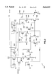
- FIG. 1 is a simplified schematic showing the high gain feedback loop for a bandgap voltage reference circuit in accordance with the present invention and which includes a current reference circuit.
- FIG. 2 is a schematic diagram illustrating a CMOS version of a bandgap voltage reference with a high gain feedback loop in accordance with the present invention and which shows a low-power voltage output comparator.
- FIG. 3 is a simplified schematic diagram illustrating another embodiment of a bandgap reference circuit with a high gain feedback loop in accordance with the present invention which is shown with current reference signals supplied by a current reference external to the bandgap voltage reference circuit.
- FIG. 4 is a schematic diagram illustrating another embodiment of a bandgap voltage reference circuit with a high gain feedback loop in accordance with the present invention which is shown with current reference signals supplied by a current reference external to the bandgap voltage reference circuit and which shows a low-power voltage output comparator.
- FIG. 1 illustrates a simplified schematic diagram of the ⁇ V BE portion of a bandgap voltage reference circuit 100 with a high gain feedback loop driven by a voltage output comparator 10 in accordance with the present invention.
- the currents I a and I b flow in PN diodes 12 and 13, respectively.
- the emitter area of diode 13 is 10 times that of diode 12.
- Voltage V a is developed across diode 12 and appears at circuit node 15.
- Voltage V b is developed across the series combination of diode 13 and resistor R4 so that this voltage appears at circuit node 16.
- Resistors R2 and R3 function primarily to determine the levels of currents I b and Ia, respectively, which, in the preferred embodiment of the invention, are made equal.
- a voltage output comparator 10 has its differential inputs connected to nodes 15 and 16 and its voltage output 11 connected to control the current input I s shown in FIG. 1.
- a current reference circuit made up of p-channel reference transistor P1, p-channel current mirror transistor P2, n-channel current reference transistor N1, n-channel current mirror transistor N2, and current reference circuit resistor R1 establish a reference current I.
- the reference current I in transistor P1 is mirrored and ratioed in p-channel current mirror transistor P3 to control current I s which is the current source for the resistor and divider network of the bandgap voltage reference circuit.
- Resistor R1 is sized such that the reference current I established by the current reference circuit is insufficient to achieve balance between voltages V a and V b , at circuit nodes 15 and 16 respectively, which are input to voltage output comparator 10.
- the comparator 10 monitors the voltages V a and V b in the bandgap circuit and generates feedback control signal 11 which controls the conductance of a current shunt transistor N3.
- Transistor N3 in turn, produces a current I 3 which shunts the resistor R1 in the current reference.
- I 3 By varying the magnitude of I 3 , the current in transistor P1 and the mirror current I s in transistor P3 can be modified which controls the currents I a and I b in the two branches of the bandgap voltage reference.
- the voltages V a and V b vary in response to currents I a and I b , respectively, to complete the feedback loop.
- the feedback causes the shunt transistor N3 to conduct the correct amount of current to balance voltages V a and V b at the inputs to comparator 10.
- the high sensitivity of the shunt transistor N3 to the voltage output 11 from comparator 10 gives the feedback loop very high gain.
- the schematic for an embodiment of the bandgap voltage reference circuit 100 is shown in FIG. 2.
- the resistors R2, R3 and R4 in the bandgap branches are formed by four smaller resistors R200, R202, R203 and R204 to save die area.
- a startup transistor N210 is shown that is driven by a Startup signal to ensure that current flow is established in the current reference circuit.
- Diode 13 is fabricated as a plurality of ten diode-connected transistors of the same size as diode-connected transistor 12 connected in parallel to produce the equivalent of a large diode with a PN junction area ten times that of diode-connected transistor 12.
- Input transistors 224 and 226 are native devices connected together at their sources and also to the drain of current mirror transistor 228.
- Current mirror transistor 228 has its gate connected to an n-channel current reference voltage Nmr which is obtained from the current reference circuit, as shown here, or from an external current reference, as described below.
- the input transistors 224 and 226 are connected to load transistors 220 and 222 respectively.
- the load transistors 220 and 222 are driven by p-channel current reference voltage Pmr which is obtained from the current reference circuit, as shown here, or from an external current reference.
- each input transistor 224 and 226 Branching off from the drain of each input transistor 224 and 226 is a clamped-active p-channel transistor (230 and 234, respectively) in series with an n-channel transistor (232 and 236, respectively).
- the clamped-active transistors 230 and 234 each have their gate connected to the ground potential and function to maintain the input transistors in their active region by preventing the drain voltage of the input transistors from falling below one p-channel threshold voltage.
- N-channel transistor 236 is diode connected and connected to the gate of transistor 232 which will consequently mirror the current in transistor 236.
- the current reference voltages will induce a current of magnitude I in transistor 228 and in each of load transistors 220 and 222. Because transistor 228 can only sink current I, the remaining current sourced by load transistors 220 and 222 must be sunk by the branch legs off of each input transistor 224 and 226. With the circuit at balance, I/2 flows through the branch leg including clamped-active transistor 234 and diode connected transistor 236. Current mirror transistor 232 mirrors the current in transistor 236 so that I/2 flows in clamped-active transistor 230 and transistor 232.
- the circuit nodes 15 and 16 of the bandgap voltage reference are connected to the input transistors 224 and 226 of the voltage comparator.
- the voltage output control signal 11 of the comparator drives the gate of shunt transistor N3 to control the current in transistor N1 and, consequently, also the current in transistor P3 to form the high gain feedback loop described above.
- the signal V ref is the stable voltage reference level generated by the circuit 200.
- the circuit of FIG. 2 may be formed using CMOS technology employing the following components:
- Transistors 224 and 226 are constructed to have low (about 0.2 volt) thresholds.
- the nominal operating power supply voltage range is 1.5-6.0 volts.
- the current in transistor P3 is 12 microamperes.
- the current "I" in transistor P1 is 2.4 microamperes (i.e., 10/50 of 12 microamperes).
- FIG. 3 a simplified schematic of a bandgap voltage reference circuit 300 with an externally controlled current source S1 is shown.
- the reference circuit 300 may be employed which is simplified version of the bandgap voltage reference circuit 100 of FIGS. 1 and 2 and requires no startup signal.
- the current sink S1 sinks a current I which, as was the case above, induces current I s in transistor P3 that is less than the current necessary to balance voltages V a and V b in the two legs of the bandgap reference circuit.
- Voltages V a and V b are input to comparator 10 which produces voltage output control 11 that drives shunt transistor N3 in order to vary the current I 3 and thereby form the high gain feedback loop discussed above.
- FIG. 4 is a detailed schematic of a bandgap voltage reference 400 which implements the design of FIG. 3.
- the current source S1 is driven by externally supplied n-channel current reference signal Nmr which also drives current sink transistor 428 in the voltage comparator circuit.
- externally supplied p-channel current reference signal Pmr drives load transistor 420 and 422 that source constant currents in the two branches of the voltage comparator circuit.
- the current I in current sink S1 combines with the current I 3 in shunt transistor N3 to determine the current in transistor P1 and, consequently, control the current I s supplied to the two branches of the bandgap voltage reference circuit by transistor P3 and which ultimately determines the level of the voltage V a and V b input to the comparator.
- the current I 3 in shunt transistor N3 is controlled by the voltage output control signal 11 from the comparator circuit to form the high gain feedback loop that controls the bandgap voltage circuit 400.
- the output signal V ref is the stable voltage reference output generated by the circuit 400.
- the circuit of FIG. 4 may be formed using CMOS technology employing the following components:
- Transistors 424 and 426 are constructed to have low (about 0.2 volt) thresholds.
- the nominal operating power supply voltage range and current are 1.5-6.0 volts and 15.2 microamperes, respectively.
- the current in transistor P3 is 12 microamperes.
- the current in transistor P1 i.e., the sum of currents "I” and “I 3 " in transistors S1 and N3, respectively
- the current in transistor P1 is 1.2 microamperes (i.e., 10/100 of 12 microamperes).
Landscapes
- Engineering & Computer Science (AREA)
- Physics & Mathematics (AREA)
- Microelectronics & Electronic Packaging (AREA)
- Nonlinear Science (AREA)
- Electromagnetism (AREA)
- General Physics & Mathematics (AREA)
- Radar, Positioning & Navigation (AREA)
- Automation & Control Theory (AREA)
- Control Of Electrical Variables (AREA)
Abstract
Description
______________________________________
Component          Value/Size (W/L in Microns)
______________________________________
Resistor R1        50 K ohms
Resistor R200      22 K ohms
Resistors R202 and R203
                   44 K ohms
Resistor R204      10 K ohms
Transistor N1      20/5
 Transistors  224, 226
                   25/5
Transistors N2, P1, P2, 220, 222, 228
                   10/5
 Transistors  230, 234
                   3/1
Transistor N3      5/2
 Transistors  232, 236
                   5/5
Transistor 210     3/5
Transistor P3      50/5
______________________________________
______________________________________
Component          Value/Size (W/L in Microns)
______________________________________
Resistor R400      22 K ohms
Resistors R402 and R403
                   44 K ohms
Resistor R404      10 K ohms
Transistor S1      5/10
 Transistors  424, 426
                   25/5
Transistor P1      10/5
 Transistors  430, 434
                   3/1
Transistor N3      5/2
    Transistors     420, 422, 428, 432, 436
                   5/5
Transistor P3      100/5
______________________________________
Claims (18)
Priority Applications (1)
| Application Number | Priority Date | Filing Date | Title |
|---|---|---|---|
| US08/689,311 US5686823A (en) | 1996-08-07 | 1996-08-07 | Bandgap voltage reference circuit |
Applications Claiming Priority (1)
| Application Number | Priority Date | Filing Date | Title |
|---|---|---|---|
| US08/689,311 US5686823A (en) | 1996-08-07 | 1996-08-07 | Bandgap voltage reference circuit |
Publications (1)
| Publication Number | Publication Date |
|---|---|
| US5686823A true US5686823A (en) | 1997-11-11 |
Family
ID=24767906
Family Applications (1)
| Application Number | Title | Priority Date | Filing Date |
|---|---|---|---|
| US08/689,311 Expired - Lifetime US5686823A (en) | 1996-08-07 | 1996-08-07 | Bandgap voltage reference circuit |
Country Status (1)
| Country | Link |
|---|---|
| US (1) | US5686823A (en) |
Cited By (33)
| Publication number | Priority date | Publication date | Assignee | Title |
|---|---|---|---|---|
| US5867012A (en) * | 1997-08-14 | 1999-02-02 | Analog Devices, Inc. | Switching bandgap reference circuit with compounded ΔV.sub.βΕ |
| US5877615A (en) * | 1997-11-06 | 1999-03-02 | Utek Semiconductor Corporation | Dynamic input reference voltage adjuster |
| US5900774A (en) * | 1996-11-28 | 1999-05-04 | Daewoo Electronics Co., Ltd. | Direct current differential base voltage generating circuit |
| US5949277A (en) * | 1997-10-20 | 1999-09-07 | Vlsi Technology, Inc. | Nominal temperature and process compensating bias circuit |
| US6150871A (en) * | 1999-05-21 | 2000-11-21 | Micrel Incorporated | Low power voltage reference with improved line regulation |
| US6181122B1 (en) | 1998-08-28 | 2001-01-30 | Globespan, Inc. | System and method for starting voltage and current controlled elements |
| US6215291B1 (en) * | 1999-01-21 | 2001-04-10 | National Semiconductor Incorporated | Reference voltage circuit |
| US6262568B1 (en) * | 1999-12-14 | 2001-07-17 | Matsushita Electric Industrial Co., Ltd. | Common mode bias generator |
| US6344770B1 (en) * | 1999-09-02 | 2002-02-05 | Shenzhen Sts Microelectronics Co. Ltd | Bandgap reference circuit with a pre-regulator |
| US6373328B2 (en) * | 1998-12-21 | 2002-04-16 | Fairchild Semiconductor Corporation | Comparator circuit |
| US6392470B1 (en) * | 2000-09-29 | 2002-05-21 | International Business Machines Corporation | Bandgap reference voltage startup circuit |
| US6465997B2 (en) * | 2000-09-15 | 2002-10-15 | Stmicroelectronics S.A. | Regulated voltage generator for integrated circuit |
| US6535435B2 (en) * | 1997-06-16 | 2003-03-18 | Hitachi, Ltd. | Reference voltage generator permitting stable operation |
| US6630859B1 (en) | 2002-01-24 | 2003-10-07 | Taiwan Semiconductor Manufacturing Company | Low voltage supply band gap circuit at low power process |
| US20040140844A1 (en) * | 2003-01-17 | 2004-07-22 | International Rectifier Corporation | Temperature compensated bandgap voltage references |
| US6784652B1 (en) * | 2003-02-25 | 2004-08-31 | National Semiconductor Corporation | Startup circuit for bandgap voltage reference generator |
| US20040239414A1 (en) * | 2003-05-30 | 2004-12-02 | Oki Electric Industry Co., Ltd. | Constant-voltage circuit |
| US20050001671A1 (en) * | 2003-06-19 | 2005-01-06 | Rohm Co., Ltd. | Constant voltage generator and electronic equipment using the same |
| US20080129271A1 (en) * | 2006-12-04 | 2008-06-05 | International Business Machines Corporation | Low Voltage Reference System |
| CN100435060C (en) * | 2002-07-23 | 2008-11-19 | 因芬尼昂技术股份公司 | Bandgap Reference Circuit |
| US20080297131A1 (en) * | 2007-06-01 | 2008-12-04 | Faraday Technology Corp. | Bandgap reference circuit |
| US20080309308A1 (en) * | 2007-06-15 | 2008-12-18 | Scott Lawrence Howe | High current drive bandgap based voltage regulator |
| US20090115775A1 (en) * | 2007-11-06 | 2009-05-07 | Himax Technologies Limited | Control circuit for a bandgap circuit |
| US20090115774A1 (en) * | 2007-11-05 | 2009-05-07 | Himax Technologies Limited | Control circuit for a bandgap circuit |
| US7567063B1 (en) | 2004-05-05 | 2009-07-28 | National Semiconductor Corporation | System and method for minimizing power consumption of a reference voltage circuit |
| US20110037451A1 (en) * | 2009-08-14 | 2011-02-17 | Fujitsu Semiconductor Limited | Bandgap voltage reference circuit |
| US20110057825A1 (en) * | 2009-09-08 | 2011-03-10 | Dialog Semiconductor Gmbh | Diode smart track |
| US20110156690A1 (en) * | 2008-09-05 | 2011-06-30 | Panasonic Corporation | Reference voltage generation circuit |
| US20150061631A1 (en) * | 2013-09-03 | 2015-03-05 | Lapis Semiconductor Co., Ltd. | Semiconductor device and current amount control method |
| CN113539307A (en) * | 2020-04-17 | 2021-10-22 | 美光科技公司 | Current regulation technique based on operating parameters |
| US20210365062A1 (en) * | 2017-11-30 | 2021-11-25 | Taiwan Semiconductor Manufacturing Company, Ltd. | Bandgap reference circuit |
| US20230253928A1 (en) * | 2022-01-24 | 2023-08-10 | Micron Technology, Inc. | Current tracking bulk voltage generator |
| US12543931B2 (en) | 2013-05-17 | 2026-02-10 | Endochoice, Inc. | Endoscope control unit with braking system |
Citations (31)
| Publication number | Priority date | Publication date | Assignee | Title |
|---|---|---|---|---|
| US4151482A (en) * | 1978-02-17 | 1979-04-24 | Rca Corporation | Folded-cascode amplifier stages |
| US4251743A (en) * | 1977-10-28 | 1981-02-17 | Nippon Electric Co., Ltd. | Current source circuit |
| US4287439A (en) * | 1979-04-30 | 1981-09-01 | Motorola, Inc. | MOS Bandgap reference |
| US4399398A (en) * | 1981-06-30 | 1983-08-16 | Rca Corporation | Voltage reference circuit with feedback circuit |
| US4447784A (en) * | 1978-03-21 | 1984-05-08 | National Semiconductor Corporation | Temperature compensated bandgap voltage reference circuit |
| US4628248A (en) * | 1985-07-31 | 1986-12-09 | Motorola, Inc. | NPN bandgap voltage generator |
| US4656374A (en) * | 1985-06-17 | 1987-04-07 | National Semiconductor Corporation | CMOS low-power TTL-compatible input buffer |
| US4816742A (en) * | 1988-02-16 | 1989-03-28 | North American Philips Corporation, Signetics Division | Stabilized current and voltage reference sources |
| US4839535A (en) * | 1988-02-22 | 1989-06-13 | Motorola, Inc. | MOS bandgap voltage reference circuit |
| US4849684A (en) * | 1988-11-07 | 1989-07-18 | American Telephone And Telegraph Company, At&T Bell Laaboratories | CMOS bandgap voltage reference apparatus and method |
| US4896094A (en) * | 1989-06-30 | 1990-01-23 | Motorola, Inc. | Bandgap reference circuit with improved output reference voltage |
| US4924113A (en) * | 1988-07-18 | 1990-05-08 | Harris Semiconductor Patents, Inc. | Transistor base current compensation circuitry |
| US4935690A (en) * | 1988-10-31 | 1990-06-19 | Teledyne Industries, Inc. | CMOS compatible bandgap voltage reference |
| US4939442A (en) * | 1989-03-30 | 1990-07-03 | Texas Instruments Incorporated | Bandgap voltage reference and method with further temperature correction |
| US4977336A (en) * | 1988-03-25 | 1990-12-11 | U.S. Philips Corporation | Schmitt-trigger circuit having no discrete resistor |
| EP0415620A2 (en) * | 1989-08-31 | 1991-03-06 | Delco Electronics Corporation | Electrical circuit |
| US5038055A (en) * | 1988-12-02 | 1991-08-06 | Kabushiki Kaisha Toshiba | Peak level detecting device and method |
| US5063342A (en) * | 1988-09-19 | 1991-11-05 | U.S. Philips Corporation | Temperature threshold sensing circuit |
| US5084665A (en) * | 1990-06-04 | 1992-01-28 | Motorola, Inc. | Voltage reference circuit with power supply compensation |
| US5087831A (en) * | 1990-03-30 | 1992-02-11 | Texas Instruments Incorporated | Voltage as a function of temperature stabilization circuit and method of operation |
| US5089769A (en) * | 1990-11-01 | 1992-02-18 | Motorola Inc. | Precision current mirror |
| US5160882A (en) * | 1990-03-30 | 1992-11-03 | Texas Instruments Incorporated | Voltage generator having steep temperature coefficient and method of operation |
| US5221864A (en) * | 1991-12-17 | 1993-06-22 | International Business Machines Corporation | Stable voltage reference circuit with high Vt devices |
| US5229710A (en) * | 1991-04-05 | 1993-07-20 | Siemens Aktiengesellschaft | Cmos band gap reference circuit |
| US5245273A (en) * | 1991-10-30 | 1993-09-14 | Motorola, Inc. | Bandgap voltage reference circuit |
| US5289111A (en) * | 1991-05-17 | 1994-02-22 | Rohm Co., Ltd. | Bandgap constant voltage circuit |
| US5291122A (en) * | 1992-06-11 | 1994-03-01 | Analog Devices, Inc. | Bandgap voltage reference circuit and method with low TCR resistor in parallel with high TCR and in series with low TCR portions of tail resistor |
| US5453679A (en) * | 1994-05-12 | 1995-09-26 | National Semiconductor Corporation | Bandgap voltage and current generator circuit for generating constant reference voltage independent of supply voltage, temperature and semiconductor processing |
| US5559425A (en) * | 1992-02-07 | 1996-09-24 | Crosspoint Solutions, Inc. | Voltage regulator with high gain cascode mirror |
| US5592123A (en) * | 1995-03-07 | 1997-01-07 | Linfinity Microelectronics, Inc. | Frequency stability bootstrapped current mirror |
| US5612613A (en) * | 1993-07-09 | 1997-03-18 | Sds-Thomson Microelectronics Pte Limited | Reference voltage generation circuit |
-
1996
- 1996-08-07 US US08/689,311 patent/US5686823A/en not_active Expired - Lifetime
Patent Citations (32)
| Publication number | Priority date | Publication date | Assignee | Title |
|---|---|---|---|---|
| US4251743A (en) * | 1977-10-28 | 1981-02-17 | Nippon Electric Co., Ltd. | Current source circuit |
| US4151482A (en) * | 1978-02-17 | 1979-04-24 | Rca Corporation | Folded-cascode amplifier stages |
| US4447784A (en) * | 1978-03-21 | 1984-05-08 | National Semiconductor Corporation | Temperature compensated bandgap voltage reference circuit |
| US4447784B1 (en) * | 1978-03-21 | 2000-10-17 | Nat Semiconductor Corp | Temperature compensated bandgap voltage reference circuit |
| US4287439A (en) * | 1979-04-30 | 1981-09-01 | Motorola, Inc. | MOS Bandgap reference |
| US4399398A (en) * | 1981-06-30 | 1983-08-16 | Rca Corporation | Voltage reference circuit with feedback circuit |
| US4656374A (en) * | 1985-06-17 | 1987-04-07 | National Semiconductor Corporation | CMOS low-power TTL-compatible input buffer |
| US4628248A (en) * | 1985-07-31 | 1986-12-09 | Motorola, Inc. | NPN bandgap voltage generator |
| US4816742A (en) * | 1988-02-16 | 1989-03-28 | North American Philips Corporation, Signetics Division | Stabilized current and voltage reference sources |
| US4839535A (en) * | 1988-02-22 | 1989-06-13 | Motorola, Inc. | MOS bandgap voltage reference circuit |
| US4977336A (en) * | 1988-03-25 | 1990-12-11 | U.S. Philips Corporation | Schmitt-trigger circuit having no discrete resistor |
| US4924113A (en) * | 1988-07-18 | 1990-05-08 | Harris Semiconductor Patents, Inc. | Transistor base current compensation circuitry |
| US5063342A (en) * | 1988-09-19 | 1991-11-05 | U.S. Philips Corporation | Temperature threshold sensing circuit |
| US4935690A (en) * | 1988-10-31 | 1990-06-19 | Teledyne Industries, Inc. | CMOS compatible bandgap voltage reference |
| US4849684A (en) * | 1988-11-07 | 1989-07-18 | American Telephone And Telegraph Company, At&T Bell Laaboratories | CMOS bandgap voltage reference apparatus and method |
| US5038055A (en) * | 1988-12-02 | 1991-08-06 | Kabushiki Kaisha Toshiba | Peak level detecting device and method |
| US4939442A (en) * | 1989-03-30 | 1990-07-03 | Texas Instruments Incorporated | Bandgap voltage reference and method with further temperature correction |
| US4896094A (en) * | 1989-06-30 | 1990-01-23 | Motorola, Inc. | Bandgap reference circuit with improved output reference voltage |
| EP0415620A2 (en) * | 1989-08-31 | 1991-03-06 | Delco Electronics Corporation | Electrical circuit |
| US5087831A (en) * | 1990-03-30 | 1992-02-11 | Texas Instruments Incorporated | Voltage as a function of temperature stabilization circuit and method of operation |
| US5160882A (en) * | 1990-03-30 | 1992-11-03 | Texas Instruments Incorporated | Voltage generator having steep temperature coefficient and method of operation |
| US5084665A (en) * | 1990-06-04 | 1992-01-28 | Motorola, Inc. | Voltage reference circuit with power supply compensation |
| US5089769A (en) * | 1990-11-01 | 1992-02-18 | Motorola Inc. | Precision current mirror |
| US5229710A (en) * | 1991-04-05 | 1993-07-20 | Siemens Aktiengesellschaft | Cmos band gap reference circuit |
| US5289111A (en) * | 1991-05-17 | 1994-02-22 | Rohm Co., Ltd. | Bandgap constant voltage circuit |
| US5245273A (en) * | 1991-10-30 | 1993-09-14 | Motorola, Inc. | Bandgap voltage reference circuit |
| US5221864A (en) * | 1991-12-17 | 1993-06-22 | International Business Machines Corporation | Stable voltage reference circuit with high Vt devices |
| US5559425A (en) * | 1992-02-07 | 1996-09-24 | Crosspoint Solutions, Inc. | Voltage regulator with high gain cascode mirror |
| US5291122A (en) * | 1992-06-11 | 1994-03-01 | Analog Devices, Inc. | Bandgap voltage reference circuit and method with low TCR resistor in parallel with high TCR and in series with low TCR portions of tail resistor |
| US5612613A (en) * | 1993-07-09 | 1997-03-18 | Sds-Thomson Microelectronics Pte Limited | Reference voltage generation circuit |
| US5453679A (en) * | 1994-05-12 | 1995-09-26 | National Semiconductor Corporation | Bandgap voltage and current generator circuit for generating constant reference voltage independent of supply voltage, temperature and semiconductor processing |
| US5592123A (en) * | 1995-03-07 | 1997-01-07 | Linfinity Microelectronics, Inc. | Frequency stability bootstrapped current mirror |
Non-Patent Citations (8)
| Title |
|---|
| Chung Yu Wu et al., New Fully Differential HF CMOS OP Amp s With Efficient Common Mode Feedback , 1989 IEEE International Symposium on Circuits and Systems, vol. 3 of 3, May 1989, pp. 2076 2079. * |
| Chung-Yu Wu et al., "New Fully Differential HF CMOS OP Amp's With Efficient Common Mode Feedback", 1989 IEEE International Symposium on Circuits and Systems, vol. 3 of 3, May 1989, pp. 2076-2079. |
| D. Senderowicz et al., "PCM Telephony: Reduced Architecture for a D/A Converter and Filter Combination", IEEE Journal of Solid-State Cirucits, 25, (1990) Aug., No. 4, pp. 987-995. |
| D. Senderowicz et al., PCM Telephony: Reduced Architecture for a D/A Converter and Filter Combination , IEEE Journal of Solid State Cirucits, 25, (1990) Aug., No. 4, pp. 987 995. * |
| J. Fisher et al., "A Highly Linear CMOS Buffer Amplifier", IEEE Journal of Solid-State Circuits, vol. SC-22, No. 3, Jun. 1987, pp. 330-334. |
| J. Fisher et al., A Highly Linear CMOS Buffer Amplifier , IEEE Journal of Solid State Circuits, vol. SC 22, No. 3, Jun. 1987, pp. 330 334. * |
| M.A. Rybicki, "A Push-Pull Transconductance Amplifier with Extended Power Supply and Common Mode Range", Motorola Technical Developments, Aug. 1989, pp. 58-59. |
| M.A. Rybicki, A Push Pull Transconductance Amplifier with Extended Power Supply and Common Mode Range , Motorola Technical Developments, Aug. 1989, pp. 58 59. * |
Cited By (52)
| Publication number | Priority date | Publication date | Assignee | Title |
|---|---|---|---|---|
| US5900774A (en) * | 1996-11-28 | 1999-05-04 | Daewoo Electronics Co., Ltd. | Direct current differential base voltage generating circuit |
| US6535435B2 (en) * | 1997-06-16 | 2003-03-18 | Hitachi, Ltd. | Reference voltage generator permitting stable operation |
| US5867012A (en) * | 1997-08-14 | 1999-02-02 | Analog Devices, Inc. | Switching bandgap reference circuit with compounded ΔV.sub.βΕ |
| US5949277A (en) * | 1997-10-20 | 1999-09-07 | Vlsi Technology, Inc. | Nominal temperature and process compensating bias circuit |
| US5877615A (en) * | 1997-11-06 | 1999-03-02 | Utek Semiconductor Corporation | Dynamic input reference voltage adjuster |
| US6181122B1 (en) | 1998-08-28 | 2001-01-30 | Globespan, Inc. | System and method for starting voltage and current controlled elements |
| US6452440B2 (en) | 1998-12-21 | 2002-09-17 | Fairchild Semiconductor Corporation | Voltage divider circuit |
| US6373328B2 (en) * | 1998-12-21 | 2002-04-16 | Fairchild Semiconductor Corporation | Comparator circuit |
| US6215291B1 (en) * | 1999-01-21 | 2001-04-10 | National Semiconductor Incorporated | Reference voltage circuit |
| US6150871A (en) * | 1999-05-21 | 2000-11-21 | Micrel Incorporated | Low power voltage reference with improved line regulation |
| US6344770B1 (en) * | 1999-09-02 | 2002-02-05 | Shenzhen Sts Microelectronics Co. Ltd | Bandgap reference circuit with a pre-regulator |
| US6542027B2 (en) * | 1999-09-02 | 2003-04-01 | Shenzhen Sts Microelectronics Co. Ltd | Bandgap reference circuit with a pre-regulator |
| US6262568B1 (en) * | 1999-12-14 | 2001-07-17 | Matsushita Electric Industrial Co., Ltd. | Common mode bias generator |
| US6465997B2 (en) * | 2000-09-15 | 2002-10-15 | Stmicroelectronics S.A. | Regulated voltage generator for integrated circuit |
| US6392470B1 (en) * | 2000-09-29 | 2002-05-21 | International Business Machines Corporation | Bandgap reference voltage startup circuit |
| US6630859B1 (en) | 2002-01-24 | 2003-10-07 | Taiwan Semiconductor Manufacturing Company | Low voltage supply band gap circuit at low power process |
| CN100435060C (en) * | 2002-07-23 | 2008-11-19 | 因芬尼昂技术股份公司 | Bandgap Reference Circuit |
| US7164308B2 (en) | 2003-01-17 | 2007-01-16 | International Rectifier Corporation | Temperature compensated bandgap voltage reference |
| EP1439445A3 (en) * | 2003-01-17 | 2005-06-08 | International Rectifier Corporation | Temperature compensated bandgap voltage reference |
| US20040140844A1 (en) * | 2003-01-17 | 2004-07-22 | International Rectifier Corporation | Temperature compensated bandgap voltage references |
| US6784652B1 (en) * | 2003-02-25 | 2004-08-31 | National Semiconductor Corporation | Startup circuit for bandgap voltage reference generator |
| US6940335B2 (en) * | 2003-05-30 | 2005-09-06 | Oki Electric Industry Co., Ltd. | Constant-voltage circuit |
| US20040239414A1 (en) * | 2003-05-30 | 2004-12-02 | Oki Electric Industry Co., Ltd. | Constant-voltage circuit |
| US20050001671A1 (en) * | 2003-06-19 | 2005-01-06 | Rohm Co., Ltd. | Constant voltage generator and electronic equipment using the same |
| US7023181B2 (en) * | 2003-06-19 | 2006-04-04 | Rohm Co., Ltd. | Constant voltage generator and electronic equipment using the same |
| US20060125461A1 (en) * | 2003-06-19 | 2006-06-15 | Rohm Co., Ltd. | Constant voltage generator and electronic equipment using the same |
| US7151365B2 (en) | 2003-06-19 | 2006-12-19 | Rohm Co., Ltd. | Constant voltage generator and electronic equipment using the same |
| US7567063B1 (en) | 2004-05-05 | 2009-07-28 | National Semiconductor Corporation | System and method for minimizing power consumption of a reference voltage circuit |
| US7825639B1 (en) | 2004-05-05 | 2010-11-02 | National Semiconductor Corporation | Minimizing power consumption of a reference voltage circuit using a capacitor |
| US20080129271A1 (en) * | 2006-12-04 | 2008-06-05 | International Business Machines Corporation | Low Voltage Reference System |
| US7834610B2 (en) * | 2007-06-01 | 2010-11-16 | Faraday Technology Corp. | Bandgap reference circuit |
| US20080297131A1 (en) * | 2007-06-01 | 2008-12-04 | Faraday Technology Corp. | Bandgap reference circuit |
| US20080309308A1 (en) * | 2007-06-15 | 2008-12-18 | Scott Lawrence Howe | High current drive bandgap based voltage regulator |
| US8427129B2 (en) | 2007-06-15 | 2013-04-23 | Scott Lawrence Howe | High current drive bandgap based voltage regulator |
| US20090115774A1 (en) * | 2007-11-05 | 2009-05-07 | Himax Technologies Limited | Control circuit for a bandgap circuit |
| US8040340B2 (en) * | 2007-11-05 | 2011-10-18 | Himax Technologies Limited | Control circuit having a comparator for a bandgap circuit |
| US20090115775A1 (en) * | 2007-11-06 | 2009-05-07 | Himax Technologies Limited | Control circuit for a bandgap circuit |
| US8093881B2 (en) | 2008-09-05 | 2012-01-10 | Panasonic Corporation | Reference voltage generation circuit with start-up circuit |
| US20110156690A1 (en) * | 2008-09-05 | 2011-06-30 | Panasonic Corporation | Reference voltage generation circuit |
| US20110037451A1 (en) * | 2009-08-14 | 2011-02-17 | Fujitsu Semiconductor Limited | Bandgap voltage reference circuit |
| US8933682B2 (en) * | 2009-08-14 | 2015-01-13 | Spansion Llc | Bandgap voltage reference circuit |
| US20110057825A1 (en) * | 2009-09-08 | 2011-03-10 | Dialog Semiconductor Gmbh | Diode smart track |
| US7936292B2 (en) | 2009-09-08 | 2011-05-03 | Dialog Semiconductor Gmbh | Diode smart track |
| EP2296281A1 (en) * | 2009-09-08 | 2011-03-16 | Dialog Semiconductor GmbH | Logarithmic DAC with diode |
| US12543931B2 (en) | 2013-05-17 | 2026-02-10 | Endochoice, Inc. | Endoscope control unit with braking system |
| US20150061631A1 (en) * | 2013-09-03 | 2015-03-05 | Lapis Semiconductor Co., Ltd. | Semiconductor device and current amount control method |
| US9454165B2 (en) * | 2013-09-03 | 2016-09-27 | Lapis Semiconductor Co., Ltd. | Semiconductor device and current control method that controls amount of current used for voltage generation based on connection state of external capacitor |
| US20210365062A1 (en) * | 2017-11-30 | 2021-11-25 | Taiwan Semiconductor Manufacturing Company, Ltd. | Bandgap reference circuit |
| US11614764B2 (en) * | 2017-11-30 | 2023-03-28 | Taiwan Semiconductor Manufacturing Company Ltd. | Bandgap reference circuit |
| CN113539307A (en) * | 2020-04-17 | 2021-10-22 | 美光科技公司 | Current regulation technique based on operating parameters |
| US20230253928A1 (en) * | 2022-01-24 | 2023-08-10 | Micron Technology, Inc. | Current tracking bulk voltage generator |
| US12132451B2 (en) * | 2022-01-24 | 2024-10-29 | Micron Technology, Inc. | Current tracking bulk voltage generator |
Similar Documents
| Publication | Publication Date | Title |
|---|---|---|
| US5686823A (en) | Bandgap voltage reference circuit | |
| US5453679A (en) | Bandgap voltage and current generator circuit for generating constant reference voltage independent of supply voltage, temperature and semiconductor processing | |
| JP3586073B2 (en) | Reference voltage generation circuit | |
| US10222819B2 (en) | Fractional bandgap reference voltage generator | |
| US6799889B2 (en) | Temperature sensing apparatus and methods | |
| US7078958B2 (en) | CMOS bandgap reference with low voltage operation | |
| US11137788B2 (en) | Sub-bandgap compensated reference voltage generation circuit | |
| US7755344B2 (en) | Ultra low-voltage sub-bandgap voltage reference generator | |
| US5059890A (en) | Constant current source circuit | |
| US5568045A (en) | Reference voltage generator of a band-gap regulator type used in CMOS transistor circuit | |
| EP0778510B1 (en) | Highly symmetrical bi-directional current sources | |
| US20040124825A1 (en) | Cmos voltage bandgap reference with improved headroom | |
| US20080224761A1 (en) | Opamp-less bandgap voltage reference with high psrr and low voltage in cmos process | |
| US4906863A (en) | Wide range power supply BiCMOS band-gap reference voltage circuit | |
| US8269478B2 (en) | Two-terminal voltage regulator with current-balancing current mirror | |
| KR20000022517A (en) | Precision bandgap reference circuit | |
| US20200192414A1 (en) | Sub-bandgap reference voltage source | |
| US20170147028A1 (en) | Low voltage current mode bandgap circuit and method | |
| US10496122B1 (en) | Reference voltage generator with regulator system | |
| US10379567B2 (en) | Bandgap reference circuitry | |
| JPH06110570A (en) | Low-power vcc/two-generator | |
| US5841271A (en) | Test mode power circuit for integrated-circuit chip | |
| US5635869A (en) | Current reference circuit | |
| US5483196A (en) | Amplifier architecture and application thereof to a band-gap voltage generator | |
| US6476669B2 (en) | Reference voltage adjustment |
Legal Events
| Date | Code | Title | Description |
|---|---|---|---|
| AS | Assignment |
Owner name: NATIONAL SEMICONDUCTOR CORPORATION, CALIFORNIA Free format text: ASSIGNMENT OF ASSIGNORS INTEREST;ASSIGNOR:RAPP, A. KARL;REEL/FRAME:008096/0424 Effective date: 19960805 |
|
| STCF | Information on status: patent grant |
Free format text: PATENTED CASE |
|
| REFU | Refund |
Free format text: REFUND - SURCHARGE FOR LATE PAYMENT, LARGE ENTITY (ORIGINAL EVENT CODE: R186); ENTITY STATUS OF PATENT OWNER: LARGE ENTITY |
|
| FPAY | Fee payment |
Year of fee payment: 4 |
|
| FPAY | Fee payment |
Year of fee payment: 8 |
|
| FPAY | Fee payment |
Year of fee payment: 12 |