US5684390A - Active semiconductor device with matched reference component maintained in breakdown mode - Google Patents
Active semiconductor device with matched reference component maintained in breakdown mode Download PDFInfo
- Publication number
- US5684390A US5684390A US08/583,114 US58311496A US5684390A US 5684390 A US5684390 A US 5684390A US 58311496 A US58311496 A US 58311496A US 5684390 A US5684390 A US 5684390A
- Authority
- US
- United States
- Prior art keywords
- voltage
- semiconductor device
- active semiconductor
- reference component
- breakdown
- Prior art date
- Legal status (The legal status is an assumption and is not a legal conclusion. Google has not performed a legal analysis and makes no representation as to the accuracy of the status listed.)
- Expired - Fee Related
Links
Images
Classifications
-
- H—ELECTRICITY
- H03—ELECTRONIC CIRCUITRY
- H03K—PULSE TECHNIQUE
- H03K17/00—Electronic switching or gating, i.e. not by contact-making and –breaking
- H03K17/14—Modifications for compensating variations of physical values, e.g. of temperature
- H03K17/145—Modifications for compensating variations of physical values, e.g. of temperature in field-effect transistor switches
-
- H—ELECTRICITY
- H03—ELECTRONIC CIRCUITRY
- H03K—PULSE TECHNIQUE
- H03K19/00—Logic circuits, i.e. having at least two inputs acting on one output; Inverting circuits
- H03K19/003—Modifications for increasing the reliability for protection
- H03K19/00369—Modifications for compensating variations of temperature, supply voltage or other physical parameters
- H03K19/00384—Modifications for compensating variations of temperature, supply voltage or other physical parameters in field effect transistor circuits
Definitions
- This invention relates to an optimization circuit for use with an active semi-conductor device, such as a MOS or CMOS field effect transistor circuit.
- guard banding has been employed to distance the circuit operating conditions from the minimum breakdown voltage but inevitably speed performance is adversely affected. There is a trade-off between performance and reject rate. The smaller the guard band, the better the performance but the higher the reject rate. In the production of any semi-conductor device, the objective is to obtain the lowest reject rate, or highest yield, possible.
- GB 2 146 145 describes an internal high voltage regulator for integrated circuits, which includes matched components that are designed to breakdown first in the event of an excessive internal programming voltage, thereby protecting the operating circuitry. This patent does not disclose how to optimize the performance of a circuit.
- the object of the invention is to alleviate the aforementioned problems.
- a method of improving the performance of an active semiconductor device with a voltage-controllable channel length comprising providing a matched reference component having similar operating characteristics to said active semiconductor device, characterized in that a current is supplied to said matched reference component to cause the breakdown thereof, the breakdown voltage of said matched reference component is continually monitored, and the operating voltage of said active semiconductor device is continually maintained to lie just below the voltage at which breakdown occurs.
- the invention can be applied to any electrical circuit which has well matched active components.
- the operating voltage can be set by a linear voltage control circuit comprising an amplifier and a power transistor forming a pass element.
- the function of the pass element is to reduce the voltage to a value of V o below the reference device breakdown voltage.
- the same technique can be used or an operational amplifier can be used to buffer the reference voltage, with the required voltage drop being obtained from a level shifting circuit.
- the reference device is preferably maintained in close physical proximity on the same circuit to the active device.
- the reference component is influenced by the same external factors as the active component and consequently its breakdown voltage varies in a similar fashion.
- a small current is forced through the reference component with a current limiting device to cause it to breakdown, and the breakdown voltage is then presented to an input of an operational amplifier, which at its output provides a control voltage.
- the invention provides an optimization circuit comprising an active semiconductor device having a channel with an identifiable breakdown voltage, a voltage regulator for applying a desired output voltage to said device, said output voltage determining the length of said channel, and a matched reference component having similar operating characteristics to said active device, characterized in that it further comprises means for supplying current to said matched reference component to cause it to break down, means for continually monitoring the breakdown voltage of said matched reference component, and means for adjusting the voltage applied to said active device by said voltage regulator to maintain the output voltage of said device at a level just below below the voltage at which breakdown occurs.
- the described circuit has the advantage that each semi-conductor device is operated as close as possible to the optimum breakdown voltage without actually causing breakdown. As a result, regardless of processing variations, the circuit will always operate very close to the maximum possible speed.
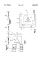
- FIG. 1 is a generalized block diagram of an optimization circuit in accordance with the invention.
- FIG. 2 shows a circuit detail of an alternative embodiment, in which the reference device is designed to breakdown at a voltage lower than the active circuit devices so as to eliminate the need for a pass element.
- an unregulated input voltage V is applied to a pass element 1 and current limiter 2.
- the current limiter 2 forces a small current through matched reference component 3, causing it to break down.
- the matched reference component 3 is chosen to have operating characteristics as close as possible to an active channel device 4, such as a CMOS FET.
- the matched component 3 is also placed in close physical proximity to the device 4 so as to be influenced by the same external factors. The matched reference component therefore behaves in the same manner as the active device 4.
- the breakdown voltage of the matched reference component 3 is continually presented to a non-inverting input of operational amplifier 5 having an inverting input connected to the mid-point of a potential divider formed by resistors 6, 7.
- the output of operational amplifier 5 is connected to the output of pass element 1.
- the operational amplifier 5 is connected as a voltage regulator in which the potential divider can be adjusted to set the voltage Vo' to be close to the matched reference voltage.
- Level shifter 8 then sets the voltage drop to a value Vo, which is just below the breakdown voltage of the frequency limiting circuitry.
- FIG. 2 shows an alternative implementation of the optimization circuit.
- the reference circuit comprises a reference MOS FET 11 connected in series with a load 14, which may be a resistor or MOS transistor, for supplying a small current to the reference MOS FET 11.
- L a is the critical channel length at which breakdown occurs of the critical transistors in the active circuit, i.e. normally the smallest channel length permitted for the process used
- ⁇ is a small increment in the order of 10% L a .
- the small reduction in channel length ⁇ ensures that the reference device breaks down at a slightly lower voltage than the active circuit devices. This arrangement eliminates the need for a pass element or level shifting circuit, but the matching characteristics still remain very good.
- Operational amplifier 15 has transistors with a
- the active circuit has a first set of non-critical transistors (not shown) that are operated with channel lengths L such that L>L a , and these transistors are supplied by the external supply 13.
- a second set of critical transistors (not shown) are operated with channel lengths L a , and these are supplied by the output 16 of the operational amplifier 15, which has one input connected to the reference MOSFET 11.
Landscapes
- Physics & Mathematics (AREA)
- Engineering & Computer Science (AREA)
- Computer Hardware Design (AREA)
- Computing Systems (AREA)
- General Engineering & Computer Science (AREA)
- Mathematical Physics (AREA)
- Amplifiers (AREA)
- Semiconductor Integrated Circuits (AREA)
- Continuous-Control Power Sources That Use Transistors (AREA)
Abstract
Description
Claims (10)
Applications Claiming Priority (3)
| Application Number | Priority Date | Filing Date | Title |
|---|---|---|---|
| CA002100727A CA2100727C (en) | 1993-07-16 | 1993-07-16 | Optimization circuit |
| CA2100727 | 1993-07-16 | ||
| PCT/CA1994/000378 WO1995002859A1 (en) | 1993-07-16 | 1994-07-13 | Optimization circuit |
Publications (1)
| Publication Number | Publication Date |
|---|---|
| US5684390A true US5684390A (en) | 1997-11-04 |
Family
ID=4151938
Family Applications (1)
| Application Number | Title | Priority Date | Filing Date |
|---|---|---|---|
| US08/583,114 Expired - Fee Related US5684390A (en) | 1993-07-16 | 1994-07-13 | Active semiconductor device with matched reference component maintained in breakdown mode |
Country Status (6)
| Country | Link |
|---|---|
| US (1) | US5684390A (en) |
| EP (1) | EP0708939B1 (en) |
| JP (1) | JPH09509267A (en) |
| CA (1) | CA2100727C (en) |
| DE (1) | DE69403661T2 (en) |
| WO (1) | WO1995002859A1 (en) |
Cited By (2)
| Publication number | Priority date | Publication date | Assignee | Title |
|---|---|---|---|---|
| US20060108990A1 (en) * | 2004-11-20 | 2006-05-25 | Hon Hai Precision Industry Co., Ltd. | Linearly regulated power supply |
| US7183756B1 (en) * | 2003-02-12 | 2007-02-27 | Nxp Bv | Current monitoring system using bi-directional current sensor |
Citations (8)
| Publication number | Priority date | Publication date | Assignee | Title |
|---|---|---|---|---|
| FR2292280A1 (en) * | 1974-11-21 | 1976-06-18 | Ibm | COMPENSATOR IN LSI TECHNOLOGY TO REMEDY FOR VARIATIONS IN CERTAIN PARAMETERS DUE TO THE MANUFACTURING PROCESS |
| US4158804A (en) * | 1977-08-10 | 1979-06-19 | General Electric Company | MOSFET Reference voltage circuit |
| US4260946A (en) * | 1979-03-22 | 1981-04-07 | Rca Corporation | Reference voltage circuit using nested diode means |
| GB2146145A (en) * | 1983-08-31 | 1985-04-11 | Nat Semiconductor Corp | Internal high voltage regulator for integrated circuits |
| EP0214899A1 (en) * | 1985-08-16 | 1987-03-18 | Fujitsu Limited | Semiconductor device having means for regulating power supply voltage applied thereto |
| US4731574A (en) * | 1983-11-15 | 1988-03-15 | Sgs-Ates Deutschland Halbleiter Bauelemente Gmbh | Series voltage regulator with limited current consumption at low input voltages |
| US5355078A (en) * | 1992-07-31 | 1994-10-11 | Sharp Kabushiki Kaisha | Semiconductor integrated circuit for a stabilized power supply circuit |
| US5548205A (en) * | 1993-11-24 | 1996-08-20 | National Semiconductor Corporation | Method and circuit for control of saturation current in voltage regulators |
-
1993
- 1993-07-16 CA CA002100727A patent/CA2100727C/en not_active Expired - Fee Related
-
1994
- 1994-07-13 JP JP7504257A patent/JPH09509267A/en active Pending
- 1994-07-13 WO PCT/CA1994/000378 patent/WO1995002859A1/en not_active Ceased
- 1994-07-13 US US08/583,114 patent/US5684390A/en not_active Expired - Fee Related
- 1994-07-13 EP EP94921556A patent/EP0708939B1/en not_active Expired - Lifetime
- 1994-07-13 DE DE69403661T patent/DE69403661T2/en not_active Expired - Fee Related
Patent Citations (11)
| Publication number | Priority date | Publication date | Assignee | Title |
|---|---|---|---|---|
| FR2292280A1 (en) * | 1974-11-21 | 1976-06-18 | Ibm | COMPENSATOR IN LSI TECHNOLOGY TO REMEDY FOR VARIATIONS IN CERTAIN PARAMETERS DUE TO THE MANUFACTURING PROCESS |
| US3970875A (en) * | 1974-11-21 | 1976-07-20 | International Business Machines Corporation | LSI chip compensator for process parameter variations |
| US4158804A (en) * | 1977-08-10 | 1979-06-19 | General Electric Company | MOSFET Reference voltage circuit |
| US4260946A (en) * | 1979-03-22 | 1981-04-07 | Rca Corporation | Reference voltage circuit using nested diode means |
| GB2146145A (en) * | 1983-08-31 | 1985-04-11 | Nat Semiconductor Corp | Internal high voltage regulator for integrated circuits |
| US4581672A (en) * | 1983-08-31 | 1986-04-08 | National Semiconductor Corporation | Internal high voltage (Vpp) regulator for integrated circuits |
| US4731574A (en) * | 1983-11-15 | 1988-03-15 | Sgs-Ates Deutschland Halbleiter Bauelemente Gmbh | Series voltage regulator with limited current consumption at low input voltages |
| EP0214899A1 (en) * | 1985-08-16 | 1987-03-18 | Fujitsu Limited | Semiconductor device having means for regulating power supply voltage applied thereto |
| US4716307A (en) * | 1985-08-16 | 1987-12-29 | Fujitsu Limited | Regulated power supply for semiconductor chips with compensation for changes in electrical characteristics or chips and in external power supply |
| US5355078A (en) * | 1992-07-31 | 1994-10-11 | Sharp Kabushiki Kaisha | Semiconductor integrated circuit for a stabilized power supply circuit |
| US5548205A (en) * | 1993-11-24 | 1996-08-20 | National Semiconductor Corporation | Method and circuit for control of saturation current in voltage regulators |
Cited By (2)
| Publication number | Priority date | Publication date | Assignee | Title |
|---|---|---|---|---|
| US7183756B1 (en) * | 2003-02-12 | 2007-02-27 | Nxp Bv | Current monitoring system using bi-directional current sensor |
| US20060108990A1 (en) * | 2004-11-20 | 2006-05-25 | Hon Hai Precision Industry Co., Ltd. | Linearly regulated power supply |
Also Published As
| Publication number | Publication date |
|---|---|
| JPH09509267A (en) | 1997-09-16 |
| DE69403661D1 (en) | 1997-07-10 |
| DE69403661T2 (en) | 1998-01-02 |
| CA2100727C (en) | 2001-06-12 |
| EP0708939B1 (en) | 1997-06-04 |
| WO1995002859A1 (en) | 1995-01-26 |
| CA2100727A1 (en) | 1995-01-17 |
| EP0708939A1 (en) | 1996-05-01 |
Similar Documents
| Publication | Publication Date | Title |
|---|---|---|
| KR100472719B1 (en) | Overcurrent protection circuit for voltage regulator | |
| US4959563A (en) | Adjustable low noise output circuit | |
| US7586716B2 (en) | Regulator with shunt over-current by-pass | |
| US4827207A (en) | Linear load current measurement circuit | |
| KR101288316B1 (en) | Linear regulator and method therefor | |
| US6917187B2 (en) | Stabilized DC power supply device | |
| US4716307A (en) | Regulated power supply for semiconductor chips with compensation for changes in electrical characteristics or chips and in external power supply | |
| JPH05315852A (en) | Current limit circuit and constant voltage source for the same | |
| US5747975A (en) | Overload protection circuit for MOS power drivers | |
| US7233462B2 (en) | Voltage regulator having overcurrent protection circuit | |
| US20060152284A1 (en) | Semiconductor device with high-breakdown-voltage regulator | |
| US8085006B2 (en) | Shunt regulator | |
| US4163161A (en) | MOSFET circuitry with automatic voltage control | |
| KR20020061877A (en) | A high power amplifier system having low power consumption and high dynamic range. | |
| US5684390A (en) | Active semiconductor device with matched reference component maintained in breakdown mode | |
| US4924120A (en) | Low noise output circuit | |
| US20060255779A1 (en) | Linear voltage regulator | |
| KR100580748B1 (en) | Gate biasing device | |
| US10778111B1 (en) | Voltage controlled adjustable current source | |
| US6307726B1 (en) | System to control the output current with temperature through a controllable current limiting circuit | |
| US11835979B2 (en) | Voltage regulator device | |
| US5864230A (en) | Variation-compensated bias current generator | |
| US6160387A (en) | Power transistor current sensing and limiting apparatus | |
| US20070080670A1 (en) | Power dissipation management in linear regulators | |
| US4419632A (en) | Bias circuit for microwave FETs |
Legal Events
| Date | Code | Title | Description |
|---|---|---|---|
| AS | Assignment |
Owner name: MITEL CORPORATION, CANADA Free format text: ASSIGNMENT OF ASSIGNORS INTEREST;ASSIGNOR:ORCHARD-WEBB, JONATHAN;REEL/FRAME:007932/0852 Effective date: 19960311 |
|
| AS | Assignment |
Owner name: CANADIAN IMPERIAL BANK OF COMMERCE, AS SECURED PAR Free format text: GRANT OF PATENT SECURITY INTEREST;ASSIGNOR:MITEL CORPORATION, A CORP. OF CANADA;REEL/FRAME:009114/0489 Effective date: 19980212 |
|
| AS | Assignment |
Owner name: MITEL CORPORATION, CANADA Free format text: RELEASE BY SECURED PARTY;ASSIGNOR:CANADIAN IMPERIAL BANK OF COMMERCE;REEL/FRAME:011590/0406 Effective date: 20010216 Owner name: MITEL, INC., A DELAWARE CORPORATION, CANADA Free format text: RELEASE BY SECURED PARTY;ASSIGNOR:CANADIAN IMPERIAL BANK OF COMMERCE;REEL/FRAME:011590/0406 Effective date: 20010216 Owner name: MITEL SEMICONDUCTOR, INC., A DELAWARE CORPORATION, Free format text: RELEASE BY SECURED PARTY;ASSIGNOR:CANADIAN IMPERIAL BANK OF COMMERCE;REEL/FRAME:011590/0406 Effective date: 20010216 Owner name: MITEL SEMICONDUCTOR, LIMITED, CANADA Free format text: RELEASE BY SECURED PARTY;ASSIGNOR:CANADIAN IMPERIAL BANK OF COMMERCE;REEL/FRAME:011590/0406 Effective date: 20010216 Owner name: MITEL TELCOM LIMITED CORPORATION, CANADA Free format text: RELEASE BY SECURED PARTY;ASSIGNOR:CANADIAN IMPERIAL BANK OF COMMERCE;REEL/FRAME:011590/0406 Effective date: 20010216 Owner name: MITEL SEMICONDUCTOR AMERICAS, INC., A DELAWARE COR Free format text: RELEASE BY SECURED PARTY;ASSIGNOR:CANADIAN IMPERIAL BANK OF COMMERCE;REEL/FRAME:011590/0406 Effective date: 20010216 |
|
| FPAY | Fee payment |
Year of fee payment: 4 |
|
| REMI | Maintenance fee reminder mailed | ||
| LAPS | Lapse for failure to pay maintenance fees | ||
| STCH | Information on status: patent discontinuation |
Free format text: PATENT EXPIRED DUE TO NONPAYMENT OF MAINTENANCE FEES UNDER 37 CFR 1.362 |
|
| FP | Expired due to failure to pay maintenance fee |
Effective date: 20051104 |