US5602401A - Data processing system and method for a surface inspection apparatus - Google Patents
Data processing system and method for a surface inspection apparatus Download PDFInfo
- Publication number
- US5602401A US5602401A US08/499,933 US49993395A US5602401A US 5602401 A US5602401 A US 5602401A US 49993395 A US49993395 A US 49993395A US 5602401 A US5602401 A US 5602401A
- Authority
- US
- United States
- Prior art keywords
- data
- size
- memory
- memories
- incoming
- Prior art date
- Legal status (The legal status is an assumption and is not a legal conclusion. Google has not performed a legal analysis and makes no representation as to the accuracy of the status listed.)
- Expired - Lifetime
Links
- 238000007689 inspection Methods 0.000 title claims abstract description 30
- 238000000034 method Methods 0.000 title claims description 16
- 230000015654 memory Effects 0.000 claims abstract description 111
- 239000002245 particle Substances 0.000 claims abstract description 101
- 239000013598 vector Substances 0.000 claims abstract description 15
- 230000005855 radiation Effects 0.000 claims abstract description 5
- 238000003672 processing method Methods 0.000 claims description 8
- 238000001514 detection method Methods 0.000 claims description 4
- 238000013507 mapping Methods 0.000 description 7
- 238000004519 manufacturing process Methods 0.000 description 4
- 241000238876 Acari Species 0.000 description 2
- 230000003247 decreasing effect Effects 0.000 description 2
- 230000007547 defect Effects 0.000 description 2
- 239000011521 glass Substances 0.000 description 2
- 238000003908 quality control method Methods 0.000 description 2
- 230000035945 sensitivity Effects 0.000 description 2
- 235000012431 wafers Nutrition 0.000 description 2
- VYZAMTAEIAYCRO-UHFFFAOYSA-N Chromium Chemical compound [Cr] VYZAMTAEIAYCRO-UHFFFAOYSA-N 0.000 description 1
- 101100386054 Saccharomyces cerevisiae (strain ATCC 204508 / S288c) CYS3 gene Proteins 0.000 description 1
- 238000004590 computer program Methods 0.000 description 1
- 238000007405 data analysis Methods 0.000 description 1
- 238000010586 diagram Methods 0.000 description 1
- 230000003292 diminished effect Effects 0.000 description 1
- 238000005192 partition Methods 0.000 description 1
- 239000010453 quartz Substances 0.000 description 1
- 239000004065 semiconductor Substances 0.000 description 1
- VYPSYNLAJGMNEJ-UHFFFAOYSA-N silicon dioxide Inorganic materials O=[Si]=O VYPSYNLAJGMNEJ-UHFFFAOYSA-N 0.000 description 1
- 230000020347 spindle assembly Effects 0.000 description 1
- 101150035983 str1 gene Proteins 0.000 description 1
- 239000000758 substrate Substances 0.000 description 1
Images


Classifications
-
- G—PHYSICS
- G01—MEASURING; TESTING
- G01N—INVESTIGATING OR ANALYSING MATERIALS BY DETERMINING THEIR CHEMICAL OR PHYSICAL PROPERTIES
- G01N21/00—Investigating or analysing materials by the use of optical means, i.e. using sub-millimetre waves, infrared, visible or ultraviolet light
- G01N21/84—Systems specially adapted for particular applications
- G01N21/88—Investigating the presence of flaws or contamination
- G01N21/94—Investigating contamination, e.g. dust
Definitions
- a data processing system and method for a surface inspection apparatus for detecting flaws and particles on a surface such as a photolithographic mask is disclosed.
- the surface of the mask is scanned by a laser beam directed to the surface and the scattering of the laser beam off the surface is analyzed: the scattering off the surface will be different if a flaw or particle is present than if no flaw or particle is present.
- the scattering can be analyzed to the point where particles or flaw are classified by size. In order to scan for and detect very small particles (e.g. 0.3 microns in diameter), it is very important that the laser beam be focused to form a very small spot size.
- Prior surface inspection apparatus utilized various signal processing routines and computer programs to process and analyze the particle data (e.g., size and position) thereby providing the user with a computer generated map which shows the relative size and position of all particles on the mask. The user then uses a microscope to visually inspect any particles of interest.
- particle data e.g., size and position
- the user then uses a microscope to visually inspect any particles of interest.
- These prior systems were fairly slow. If the photolithographic mask is scanned slowly (e.g. much less than 1800 rpm) and the spot size of a laser beam is quite large (e.g. much larger than 1.7 ⁇ 5.3 micrometers) then the particle size and position data could be processed and analyzed during each scan. These low rates of scanning, however, mean that the inspection of each mask is slow and hence expensive. And, such a large laser beam spot size may fail to accurately detect very small particles.
- This invention results from the realization that although a laser beam can be focused to inspect a surface for very small particles in a very tight spiral pattern (e.g., 3 microns between successive beam traces), the final required map resolution is much larger (e.g., a 15 ⁇ 15 micron square) so there is no need to permanently record the size data for each particle during each revolution of the surface and furthermore that if the size data of a particular particle is decreasing between revolutions, there is no need to store this extraneous information thereby reducing computing time and increasing the speed of inspection.
- This invention results from the further realization that if two temporary memories are used to store size and position data, one memory can record size and position data during a number M of scans while the size and position data is transferred from the other memory to permanent memory, and then the record and transmit operations can be alternated between the two memories every M scans of the surface under inspection.
- This invention features and may, depending on the specific implementation, comprise, include, consist essentially of, or consist of a surface inspection system.
- a laser beam source There is a laser beam source; means for focusing a laser beam from the source onto the surface; means for rotating and translating the surface with respect to the means for focusing to trace a spiral pattern with the laser beam on the surface; detection means for detecting scattering of the laser beam from the surface; and means, responsive to the detection means, for calculating the size of any detected particles on the surface and for determining the position of the detected particles on the surface.
- memory means for storing the size and position data of any detected particles; and means, responsive to the memory means, for recording the size and position data of any detected particles on each revolution but transferring the stored data only once per M revolutions (e.g. five).
- the system further includes means for updating the memory means each revolution for M revolutions only if the incoming size data for a detected particle is larger than the stored size data for that particle. This saves processing time and storage space since superfluous size data
- the memory means typically includes two FIFO memories, one being read from while the second is written to. There are means for switching between the two memories every M revolutions to allow data analysis to take place simultaneously with data acquisition.
- the FIFO memories are programmed to receive data only if the incoming size data for an address space is greater than the size data stored in that address space.
- this invention features a data processing system for a surface inspection apparatus which analyzes flaws by size and position on a surface, the data processing system comprising: means for obtaining flaw size and position data from the surface inspection apparatus; first and second memories; means for writing size data to one memory while reading size data from the second memory and switching memories every M revolutions of the surface; and means for replacing a stored size datum for a given position in one of said memories during each revolution for M revolutions with an incoming size datum only if the incoming size datum is greater than the stored size datum.
- this invention features a data processing system comprising: means for counting; means for obtaining data; first and second memories; means for writing data to the first memory while reading data from the second memory and switching memories after every M counts; and means for replacing previously stored data in an address space of one of the first and second memories with incoming data only if the incoming data meets a preselected criteria.
- the data is typically size and position data and the preselected criteria is typically that the incoming size data must be greater than the stored size data.
- this invention relates to a system for processing particle size and position data for a surface under inspection.
- This system comprises means for rotating and translating a surface with respect to a beam of radiation used to detect particles on the surface; means for dividing the surface into a number N of angular vectors; means for counting the number of revolutions of the surface; means for collecting particle size and position data at each angular vector during each revolution; first and second memories having at least N address spaces, each address space allocated for a specific angular vector; means for writing the collected particle size and position data to the first memory and for reading particle size and position data from the second memory and switching memories every M revolutions; and means for storing in each address space of the memories the greater of stored size data and incoming size data.
- This invention also features a data processing method for a surface inspection apparatus which analyzes flaws by size and position on a surface, the data processing method comprising: obtaining flaw size and position data from the surface inspection apparatus; writing size data to one memory while reading size data from a second memory and switching memories every M revolutions of the surface; and replacing a stored size datum for a given position in a memory during each revolution for M revolutions with an incoming size datum only if the incoming size datum is greater than the stored size datum.
- the method involves obtaining flaw size and position data; writing the data to one memory while reading the data from a second memory and switching memories after every M counts; and replacing previously stored data in an address space of a memory with incoming data only if the incoming data meets a preselected criteria.
- the preselected criteria is usually that the incoming data must be greater than the stored data.
- the invention features a method of processing particle size and position data of particles detected on a surface under inspection, the method comprising: rotating and translating a surface with respect to a beam of radiation used to detect particles on the surface; dividing the surface into a number N of angular vectors; counting the number of revolutions of the surface; collecting flaw size and position data at each angular vector during each revolution; establishing first and second memories each having at least N address spaces, each address space allocated for a specific angular vector; writing the collected particle size and position data to the first memory and reading particle size and position data from the second memory and switching memories every M revolutions; and programming the memories to store in each the address space the greater of previously stored size data and incoming size data.
- FIG. 1 is a block diagram of a surface inspection apparatus which may incorporate the particle size and position data processing system of this invention
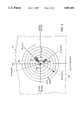
- FIG. 2 is a top view of a portion of a typical surface inspected by the surface inspection apparatus of FIG. 1;
- FIG. 3 is a schematic view of a portion of one FIFO memory of the data processing system of this invention.
- FIG. 4 is a functional flow chart of the data processing routine of this invention.
- FIG. 1 includes photolithographic mask holder 12 rotated in the direction shown by arrow 14 by air spindle 16 positioned on translation stage 18.
- Translation stage 18 is equipped with translation encoder 44 to provide information on its position in the direction shown by arrow 20.
- Laser 22, powered by power supply 24, delivers laser beam 26 through beam forming optics 28.
- Beam 26 is directed by mirror 30 to parabolic mirror 32 which focuses it on the surface of photolithographic mask 34. Scattering of the laser beam off the surface is detected by sensors 36 and 38.
- the output of sensors 36 and 38 is analyzed by processing circuit 40 to deduce the size of a particle or flaw detected on the surface of photolithographic mask 34. The position of a detected flaw or particle is determined based on signals (“counts") from rotation encoder 42 and translational encoder 44.
- Signal processing circuit subsystem 40 includes amplifiers 42 and 43 responsive to detectors 36 and 38 respectively. Detectors 36 and 38 provide an electrical signal corresponding to the intensity of light detected over lines 44 and 45 to amplifiers 42 and 43 respectively, within analog signal processing circuit 40.
- the amplified signals are provided to signal comparators banks 46 and 47. Comparators banks 46 and 47 each output a multi-bit digital word to minimizer 48. An absence of a comparator output signal indicates that none of the detectors 36 or 38 detected an intensity level which above a set threshold level. Signals that exceed the threshold level produce different digital words that correspond to the size of the signal and hence the size of the flaw detected.
- Sensitivity set-up circuit 50 enables the adjustment of the levels A-E so that an operator can vary the sensitivity level for different applications.
- the digital words corresponding to the signals detected from comparators banks 46 and 47 are provided to minimizer 48 which outputs the minimum intensity level (A-E) detected by detectors 36 and 38. If the minimum detected intensity level from minimizer 48 is equal to zero, this indicates that no defect or only a surface pattern was detected at that particular point on plate 34. If the minimum detected energy level exceeds zero, this indicates that a flaw is present.
- the levels of intensity A-E are indicative of the size of a given particle. If the intensity level on line 44 from detector 36 is level D, comparator 47 will output a D signal but if the level on line 45 from detector 38 is a level E as output by comparator 46, minimizer 48 will only present size data "D" on line 49.
- the result on line 49 is a signal S i indicative of a size of a detected particle.
- the angular position ⁇ of a detected particle i is delivered as signal ⁇ i from rotational encoder 42 on line 48.
- the radial position r of a detected particle i is provided as a signal r i on line 50 from translation encoder 44.
- One air spindle revolution is divided into 50,000 angular ⁇ data points.
- Signal processor 40 keeps track of the current angular ⁇ position of spindle 16 using rotary encoder 42 pulses (ticks) which generates an interrupt signal at every index position. In this way, the size (S) and position (r and ⁇ ) of particle 70, FIG. 2 is processed. See also U.S. Pat. Nos. 4,943,734; 4,794,264; 4,794,265; and/or 5,389,794.
- FIFO memories 52 and 54 which store the size (S) and position (r, ⁇ ) data of any detected particles and mapping computer 56 which reads the stored data once per M number of revolutions of photolithographic mask 34.
- the laser beam trace on the surface of photolithographic mask 34 forms the spiral pattern as shown at 72 with only a 3 micron spacing between heaters of adjacent traces as shown at 74.
- Beam spot size on the surface is on the order of 10 micrometer at 1/e 2 intensity level, so the trace overlap at 3 micrometer pitch occurs at approximately 80% intensity level.
- a particle can be detected during several subsequent revolutions, of which one revolution will be the most optimal, namely when the beam's most intensive center passes closets to the particle.
- the particle will be exposed to lower intensity of light at the beam's periphery, so that its scattering and thus apparent size classification will be diminished.
- Mask 34 is divided into 50,000 angular sectors. Therefore, particle 70 may be detected during 4 revolutions, corresponding to radial distances of 3 micrometer (as size "B"), 6 micrometer (as size “D”), 9 micrometer (as size “E”) and 12 micrometer, all of them at angular position of 6,000 counts (corresponding to [6,000/50,000]*360°) from reference sector 80.
- the above described radial resolution of 3 micrometer is excessive. Accordingly, in this example, the traces at 3, 6, 9, 12 and 15 micrometers are "combined" into one trace for the three particles 70, 76 and 71 at angular position of 6000, 16000 and 35000, respectively particle 71 of size B may be 0.4 micrometer in diameter, particle 75 of size C--0.5 micrometer, particle 70 of size E--1.0 micrometer in diameter.
- FIFO memories 52 and 54, FIG. 1 are programmed by the signal processing circuit to be updated only if the size data for a particle detected in a given angular sector increases between subsequent revolutions of mask 34. Also, as explained supra, mapping computer 56 automatically switches between FIFO memory 52 and FIFO memory 54 so one can be recording data while the second is transferring data permanent memory.
- address spaces 90, 94, 96, 98, 100, 102, and 104 are depicted for FIFO memory 52, FIG. 1.
- the size (A-E) of a detected particle is analyzed by processing circuit 40, FIG. 1 which alternatively transmits the size (S i ) and position (r i , ⁇ i ) data to memories 52 and 54 under the control of computer 56.
- the incoming particle size data of particle 70 is "D" and this data replaces the previous size data "B" in address space 94 for particle 70 as shown at 110 since a particle of size "D" is larger than a particle of size "B".
- the incoming size data of particle 76 is decreasing to a size "B” but since it is normally desirable to analyze only the maximum size of a given particle, the size "B” data is not stored and instead size data "C" remains in address space 98 for particle 76 as shown at 110. This is accomplished by an "OR" operation wherein the FIFO memories are programmed to automatically accept data in a given address space only if the incoming data is larger than the stored size data already in that address space.
- particle 70 is analyzed as a size "E” while particle 76 is only detected to be a size "B” but the FIFO memories again only store the larger of the incoming data as compared to already stored data as shown at 114.
- mapping computer 56 provides the user with a picture on display 57 of the position and size (by color coding) of particles 76, 70 and 71 so that quality control personnel can determine whether photolithographic mask 34 is clean enough to be used for a production run.
- mapping computer 56 This results at a significant savings of processing time since first, the extraneous size data for a given particle was never stored and second, because there are two FIFO memories 52 and 54 and one can be used to store particle size data while the other is read by mapping computer 56.
- FIG. 4 is a flow chart of the microscode in signal processing circuit 56, FIG. 1, for achieving the results shown in FIG. 3.
- the rotation counter is started as shown at 106, FIG. 3 and the size (S) and position (r, ⁇ ) of any particles detected during the first revolution as shown at 106, FIG. 3, is collected, step 142, FIG. 4, and written to one of the FIFO memories, step 144.
- the size and position data for the next revolution as shown at 108, FIG. 3, is also collected, step 146, FIG. 4, and then as shown at 110 in FIG. 3, "ORed" with the data already in the FIFO memory, step 148, FIG. 4.
- the size and position data for the next revolution is collected as shown at 112 in FIG.
- step 154 After a number of M revolutions as shown at 154, the data from that FIFO memory is transferred, step 156, to mapping computer 56, FIG. 1 and the FIFO memories are switched, step 158 and the process starts all over again at steps 140 for the next M revolutions.
- M is preferably set to 5 for system 10, FIG. 1, since the microscope used to manually inspect the surface of photolithographic mask 34 after it is automatically inspected by system 10 typically only has a resolution of about 15 microns ⁇ 15 microns and it takes 5 revolutions of photolithographic mask 34 before the laser beam covers 15 microns in the radial direction.
- FIG. 1 for each revolution of photolithographic mask 34 would involve a considerable amount of processing time and result in enormous amounts of unusable data since quality control personal are only interested locating defects with resolution of 15 ⁇ 15 um, substantially larger that 3 uu intertrace distance. Any finer resolution as far as particle position information is concerned is not required and slows down processing time thereby slowing down the rate of inspection of a series of photolithographic masks using system 10, FIG. 1.
- the following is the actual microcode operant in signal processing circuit 56, FIG. 1 to achieve the results shown in FIG. 3; ##STR1##
Landscapes
- Physics & Mathematics (AREA)
- Health & Medical Sciences (AREA)
- Life Sciences & Earth Sciences (AREA)
- Chemical & Material Sciences (AREA)
- Analytical Chemistry (AREA)
- Biochemistry (AREA)
- General Health & Medical Sciences (AREA)
- General Physics & Mathematics (AREA)
- Immunology (AREA)
- Pathology (AREA)
- Investigating Materials By The Use Of Optical Means Adapted For Particular Applications (AREA)
Abstract
Description
Claims (14)
Priority Applications (1)
| Application Number | Priority Date | Filing Date | Title |
|---|---|---|---|
| US08/499,933 US5602401A (en) | 1995-07-10 | 1995-07-10 | Data processing system and method for a surface inspection apparatus |
Applications Claiming Priority (1)
| Application Number | Priority Date | Filing Date | Title |
|---|---|---|---|
| US08/499,933 US5602401A (en) | 1995-07-10 | 1995-07-10 | Data processing system and method for a surface inspection apparatus |
Publications (1)
| Publication Number | Publication Date |
|---|---|
| US5602401A true US5602401A (en) | 1997-02-11 |
Family
ID=23987352
Family Applications (1)
| Application Number | Title | Priority Date | Filing Date |
|---|---|---|---|
| US08/499,933 Expired - Lifetime US5602401A (en) | 1995-07-10 | 1995-07-10 | Data processing system and method for a surface inspection apparatus |
Country Status (1)
| Country | Link |
|---|---|
| US (1) | US5602401A (en) |
Cited By (7)
| Publication number | Priority date | Publication date | Assignee | Title |
|---|---|---|---|---|
| US5995218A (en) * | 1997-01-17 | 1999-11-30 | Nec Corporation | Method for inspecting defects of wafer and inspection equipment thereof |
| US6256092B1 (en) * | 1997-11-28 | 2001-07-03 | Hitachi, Ltd. | Defect inspection apparatus for silicon wafer |
| US20030053046A1 (en) * | 2001-09-19 | 2003-03-20 | Mitsubishi Denki Kabushiki Kaisha | Defect inspecting device for substrate to be processed and method of manufacturing semiconductor device |
| US6813376B1 (en) * | 1999-10-29 | 2004-11-02 | Rudolph Technologies, Inc. | System and method for detecting defects on a structure-bearing surface using optical inspection |
| US20110125460A1 (en) * | 2005-12-28 | 2011-05-26 | Takashi Suzuki | Information Processing Apparatus and Apparatus for Evaluating Whether Information Processing Method is Possible |
| US20140303931A1 (en) * | 2005-12-28 | 2014-10-09 | Takashi Suzuki | Information processing apparatus and apparatus for evaluating whether an information processing method is possible |
| CN114663336A (en) * | 2020-12-22 | 2022-06-24 | 富泰华工业(深圳)有限公司 | Model input size determination method and related equipment |
Citations (2)
| Publication number | Priority date | Publication date | Assignee | Title |
|---|---|---|---|---|
| US33357A (en) * | 1861-09-24 | Improved camp cooking apparatus | ||
| US4134684A (en) * | 1977-01-18 | 1979-01-16 | Intex Corp. | Repeat defect detector system |
-
1995
- 1995-07-10 US US08/499,933 patent/US5602401A/en not_active Expired - Lifetime
Patent Citations (2)
| Publication number | Priority date | Publication date | Assignee | Title |
|---|---|---|---|---|
| US33357A (en) * | 1861-09-24 | Improved camp cooking apparatus | ||
| US4134684A (en) * | 1977-01-18 | 1979-01-16 | Intex Corp. | Repeat defect detector system |
Cited By (11)
| Publication number | Priority date | Publication date | Assignee | Title |
|---|---|---|---|---|
| US5995218A (en) * | 1997-01-17 | 1999-11-30 | Nec Corporation | Method for inspecting defects of wafer and inspection equipment thereof |
| US6256092B1 (en) * | 1997-11-28 | 2001-07-03 | Hitachi, Ltd. | Defect inspection apparatus for silicon wafer |
| US6384909B2 (en) | 1997-11-28 | 2002-05-07 | Hitachi, Ltd. | Defect inspection method and apparatus for silicon wafer |
| US6683683B2 (en) | 1997-11-28 | 2004-01-27 | Hitachi, Ltd. | Defect inspection method and apparatus for silicon wafer |
| US6813376B1 (en) * | 1999-10-29 | 2004-11-02 | Rudolph Technologies, Inc. | System and method for detecting defects on a structure-bearing surface using optical inspection |
| US20030053046A1 (en) * | 2001-09-19 | 2003-03-20 | Mitsubishi Denki Kabushiki Kaisha | Defect inspecting device for substrate to be processed and method of manufacturing semiconductor device |
| US6768542B2 (en) * | 2001-09-19 | 2004-07-27 | Renesas Technology Corp. | Defect inspecting device for substrate to be processed and method of manufacturing semiconductor device |
| US20110125460A1 (en) * | 2005-12-28 | 2011-05-26 | Takashi Suzuki | Information Processing Apparatus and Apparatus for Evaluating Whether Information Processing Method is Possible |
| US8619242B2 (en) * | 2005-12-28 | 2013-12-31 | Takashi Suzuki | Information processing apparatus and apparatus for evaluating whether information processing method is possible |
| US20140303931A1 (en) * | 2005-12-28 | 2014-10-09 | Takashi Suzuki | Information processing apparatus and apparatus for evaluating whether an information processing method is possible |
| CN114663336A (en) * | 2020-12-22 | 2022-06-24 | 富泰华工业(深圳)有限公司 | Model input size determination method and related equipment |
Similar Documents
| Publication | Publication Date | Title |
|---|---|---|
| US4626101A (en) | Surface defect inspecting apparatus | |
| US6603542B1 (en) | High sensitivity optical inspection system and method for detecting flaws on a diffractive surface | |
| EP0179309B1 (en) | Automatic defect detection system | |
| US5672885A (en) | Surface displacement detection and adjustment system | |
| US5377002A (en) | Apparatus for surface inspections | |
| US6614520B1 (en) | Method for inspecting a reticle | |
| US5625193A (en) | Optical inspection system and method for detecting flaws on a diffractive surface | |
| US5377001A (en) | Apparatus for surface inspection | |
| US7864310B2 (en) | Surface inspection method and surface inspection apparatus | |
| US4417149A (en) | Apparatus for detecting and measuring defects | |
| US4674875A (en) | Method and apparatus for inspecting surface defects on the magnetic disk file memories | |
| JP4384737B2 (en) | Inspection equipment for high-speed defect analysis | |
| JPH0862150A (en) | Disk defect inspecting apparatus | |
| US5602401A (en) | Data processing system and method for a surface inspection apparatus | |
| KR0163780B1 (en) | How to identify height using image recognition device and image recognition device to identify height | |
| JP3197329B2 (en) | Surface inspection equipment | |
| EP0094501A2 (en) | Methods of inspecting pattern masks | |
| JP3287526B2 (en) | Surface inspection method for photoconductor drum for electrophotography | |
| JPH0517482B2 (en) | ||
| JPH0431056B2 (en) | ||
| JPH067104B2 (en) | Surface inspection device | |
| JPS63317748A (en) | Display method of concentrated place of defects in map display of defect in magnetic disk | |
| McLemore et al. | Automatic surface flaw inspection of nuclear fuel pellets | |
| JP2605042B2 (en) | Magnetic defect inspection device | |
| JPH01316643A (en) | Device for inspecting fault of disk |
Legal Events
| Date | Code | Title | Description |
|---|---|---|---|
| AS | Assignment |
Owner name: QC OPTICS, INC., MASSACHUSETTS Free format text: ASSIGNMENT OF ASSIGNORS INTEREST;ASSIGNORS:BROUDE, SERGEY V.;ALLEN, NICHOLAS;BOUDOUR, ABDU;AND OTHERS;REEL/FRAME:007650/0831 Effective date: 19950913 |
|
| AS | Assignment |
Owner name: STATE STREET BANK AND TRUST COMPANY, MASSACHUSETTS Free format text: SECURITY INTEREST;ASSIGNOR:QC OPTICS, INC.;REEL/FRAME:008669/0943 Effective date: 19960329 |
|
| STCF | Information on status: patent grant |
Free format text: PATENTED CASE |
|
| FPAY | Fee payment |
Year of fee payment: 4 |
|
| AS | Assignment |
Owner name: QC OPTICS, INC., MASSACHUSETTS Free format text: DISCHARGE OF COLLATERAL ASSIGNMENT;ASSIGNOR:STATE STREET BANK AND TRUST COMPANY;REEL/FRAME:012219/0071 Effective date: 19980629 |
|
| FEPP | Fee payment procedure |
Free format text: PAYOR NUMBER ASSIGNED (ORIGINAL EVENT CODE: ASPN); ENTITY STATUS OF PATENT OWNER: LARGE ENTITY Free format text: PAYER NUMBER DE-ASSIGNED (ORIGINAL EVENT CODE: RMPN); ENTITY STATUS OF PATENT OWNER: LARGE ENTITY |
|
| FPAY | Fee payment |
Year of fee payment: 8 |
|
| FPAY | Fee payment |
Year of fee payment: 12 |
|
| REMI | Maintenance fee reminder mailed |